 | –≠–ª–µ–∫—Ç—Ä–æ–Ω–Ω—ã–π –∫–æ–º–ø–æ–Ω–µ–Ω—Ç: IL34C86N | –°–∫–∞—á–∞—Ç—å:  PDF PDF  ZIP ZIP |

IL34C86
1
Differential line receiver.
.
Microcircuit IL34C86 consists of four
differential line receivers and is a
microcircuit that meets international
standards of data transmission RS-422,
RS-423, and it is widely used in data
transmission nets, particularly in a unit for
local loop of ATS.
Functions implemented
This device carries out comparing inputs
with low differential signal of 200mV and
gives on output full signal with load
carrying capacity of
6m, and also has
hysteresis to improve noise margin.
Designation
Of microcircuit in package
IL34C86N Plastic DIP
IL34C86D SOIC
T
A
from minus 40
to plus 85
úC
for all packages
Truth table
Enable input output
L X Z
H
V
ID
ôV
TH
(max)
H
H
V
ID
òV
TH
(max)
L
H Open
*
H
V
ID
- difference of inputs A2-A1, or B2-B1, or C2-C1, or D2-D1.
V
TH
- minimum differential input voltage.
Open
*
- no signals delivered to inputs.

IL34C86
2
Purpose of pins
of pin
Symbol
Purpose
01
A1
Input of receiver A
02
A2
Input of receiver A
03
A
Output of receiver A
04
En A/C
input of switching outputs of A and C
receivers into the third state
05
C
Output of receiver C
06
C2
2 Input of receiver C
07
C1
1 Input of receiver C
08
GND General
pin
09
D1
1 Input of receiver D.
10
D2
2 Input of receiver D.
11
D
Output of receiver D.
12
En B/D
input of switching outputs of B and D
receivers into the third state
13
B
Output of receiver B.
14
B2
2 Input of receiver C
15
B1
1 Input of receiver C
16
V
CC
Pin of power supply from source of voltage
L - Low voltage level
H - High voltage level
X - any level of voltage
Z - the third state of output .
V
DD
01
02
03
04
05
06
10
11
12
13
14
15
16
07
08
09
Y3
X2
Y2
X1
V
SS
X3
B
Z3
Z2
Z1
Z0
A
Y1
X0
Y0
Figure 2 Designation of pins in package

IL34C86
3
Figure 3. Block diagram of microcircuit.
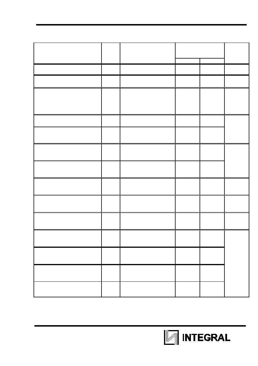
Table 1 - Limiting and extreme parameters
Parameter
Symbol
Limiting mode
Extreme mode
Units of
measureme
nt
min
max
min
max
Supply voltage
V
CC
4.50 5.50 -- 7 V
Input voltage
V
CM
-- -- -14
14
differential input voltage
V
DIFF
-- -- -14
14
Voltage on input Enable
V
IN
-- -- --
7
Output current
--
--
--
-25
+25
m
transition time when
switching in, switching
off on input Enable
t
r
, t
f
-- 500 --
--
n
Dissapated
power
DIP P
D
-- -- --
1645
*
mW
SO
--
--
--
1190
*
Operation temperature
T
A
-40 +85 -- --
ú
Storage temperature
T
STG
-- -- -65
+150
Temperature of
soldering, 4
T
L
-- -- --
260
*
- at increasing temperature higher than 25
ú P
D
decreased on 13.89mW/
úC for DIP package and on
9.80mW/
úC for SO package.
IN A2
IN A1
+
-
IN C2
IN C1
+
-
Enable
IN B2
IN B1
+
-
IN D2
IN D1
+
-
Enable
Output A
Output C
Output B
Output D
GND Vcc
IL34C86
4
Table 2 -Electric parameters
T= -40
0
ü
+85
0
C
parameter symbol
conditions
of
measurement
standard units
of
measure
ment
min max.
Minimum differential input
voltage
V
TH
-7V < V
Cm
< +7V
-200
200
mV
input resistance
R
IN
V
IN
= -7V, +7V (the rest
inputs on "ground")
5.0 10 khm
input current
I
IN
V
IN
= -10V (the rest inputs
on"ground")
V
IN
= +10V (the rest inputs
on "ground")
-- +1.5
m
--
-2.5
minimum output voltage of high
level
V
OH
V
CC
= 4.5V, V
DIFF
= +1V,
I
OUT
= -6.0hm
3.8 -- V
maximum output voltage of low
level
V
OL
V
CC
= 5.5V, V
DIFF
= -1V,
I
OUT
= +6.0hm
-- 0.3
minimum input voltage of high
level on input Enable
V
IH
-- 2.0
--
V
maximum input voltage of low
level on input Enable
V
IL
-- --
0.8
maximum output current of the
third state
I
OZ
V
OUT
= V
CC
or 0V
--
0.5
maximum input current on input
Enable
I
I
V
IN
= V
CC
or 0V
--
1.0
consumption current
I
CC
V
CC
= 5.5V, V
DIFF
= +1V
--
23
m
time of propagation delay at
switching off, switching on
t
PLH
,
t
PHL
C
L
= 50pF, V
DIFF
= 2.5V,
V
Cm
= 0V
-- 30 n
Transition time when switching
in, switching off
t
RISE
,
t
FALL
C
L
= 50pF, V
DIFF
= 2.5V,
V
Cm
= 0V
-- 9
time of the third state
propagation delay on input
Enable
t
PLZ
,
t
PHZ
C
L
= 50pF, V
DIFF
= 2.5V,
R
L
= 1000khm
-- 18
time of the third state
propagation delay on input
Enable
t
PZL
,
t
PZH
C
L
= 50pF, V
DIFF
= 2.5V,
R
L
= 1000khm
-- 21

IL34C86
5
Figure 4 - Time diagram of signals at changing dynamic parameters t
PLH
, t
PHL
, t
TLH
,
t
THL
, t
PZH
, t
PHZ
, t
PZL
, t
PLZ
t
PLH
t
PHL
Output
V- Input
V+ Input = 0 V
V
OL
V
OH
+2.5 V
-2.5 V
0 V
90 %
10 %
10 %
90 %
t
TLH
t
THL
50 %
.