 | –≠–ª–µ–∫—Ç—Ä–æ–Ω–Ω—ã–π –∫–æ–º–ø–æ–Ω–µ–Ω—Ç: IL358 | –°–∫–∞—á–∞—Ç—å:  PDF PDF  ZIP ZIP |
TECHNICAL DATA
1
Low Power Dual Operational Amplifier
The IL358 contains two independent high gain operational
amplifiers with internal frequency compensation. The two op-amps
operate over a wide voltage range from a single power supply. Also
use a split power supply. The device has low power supply current
drain, regardless of the power supply voltage. The low power drain
also makes the IL358 a good choice for battery operation.
When your project calls for a traditional op-amp function, now you
can streamline your design with a simple single power supply. Use
ordinary +5V
DC
common to practically any digital system or personal
computer application, without requiring an extra 15V power supply
just to have the interface electronics you need.
The IL358 is a versatile, rugged workhorse with a thousand-and-
one uses, from amplifying signals from a variety of transducers to dc
gain blocks, or any op-amp function. The attached pages offer some
recipes that will have your project cooking in no time.
û
Internally frequency compensated for unity gain
û
Large DC voltage gain: 100dB
û
Wide power supply range:
3V ~ 32V (or
1.5V ~
16V)
û
Input common-mode voltage range includes ground
û
Large output voltage swing: 0V DC to V
CC
-1.5V DC
û
Power drain suitable for battery operation
û
Low input offset voltage and offset current
û
Differential input voltage range equal to the power supply voltage
IL358
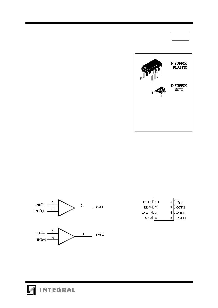
ORDERING INFORMATION
IL358N Plastic
IL358D SOIC
T
A
= 0
ú
to 70
ú
C
for all packages.
LOGIC DIAGRAM
PIN 4 = GND
PIN 8=V
CC
PIN ASSIGNMENT
IL358
2
MAXIMUM RATINGS
*
Symbol
Parameter
Value
Unit
V
CC
Power Supply Voltages
Single Supply
Split Supplies
32
16
V
V
IDR
Input Differential Voltage Range (1)
32
V
V
ICR
Input Common Mode Voltage Range
-0.3 to 32
V
I
SC
Output Short Circuit Duration
Continuous
T
J
Junction Temperature
Plastic Packages
150
ú
C
Tstg
Storage Temperature
Plastic Packages
-55 to +125
ú
C
I
IN
Input Current, per pin (2)
50
mA
T
L
Lead Temperature, 1mm from Case for 10 Seconds
260
ú
C
*
Maximum Ratings are those values beyond which damage to the device may occur.
Functional operation should be restricted to the Recommended Operating Conditions.
+Derating - Plastic DIP: - 10 mW/
ú
C from 65
ú
to 125
ú
C
SOIC Package: : - 7 mW/
ú
C from 65
ú
to 125
ú
C
Notes:
1.
Split Power Supplies.
2.
V
IN
<-0.3V. This input current will only exist when voltage at any of the input leads is driven negative.
RECOMMENDED OPERATING CONDITIONS
Symbol
Parameter
Min
Max
Unit
V
CC
DC Supply Voltage
2.5 or
5.0
15 or
30
V
T
A
Operating Temperature, All Package Types
0
+70
ú
C
This device contains protection circuitry to guard against damage due to high static voltages or electric
fields. However, precautions must be taken to avoid applications of any voltage higher than maximum rated
voltages to this high-impedance circuit. For proper operation, V
IN
and V
OUT
should be constrained to the range
GND
ò
(V
IN
or V
OUT
)
ò
V
CC
.
Unused inputs must always be tied to an appropriate logic voltage level (e.g., either GND or V
CC
).
Unused outputs must be left open.
IL358
3
DC ELECTRICAL CHARACTERISTICS
(T
A
=0 to +70
ú
C)
Guaranteed Limit
Symbol
Parameter
Test Conditions
Min
Typ
Max
Unit
V
IO
Maximum Input Offset
Voltage
V
O
=1.4V V
CC
=5.0-30V;R
S
=0
V
ICM
=0V to V
CC
-1.7V
9.0
mV
V
IO
/
T
Input Offset Voltage
Drift
R
S
=0
, V
CC
=30V
7.0
V/
ú
C
I
IO
Maximum Input Offset
Current
V
CC
=5.0V
150
nA
I
IO
/
T
Input Offset Current Drift R
S
=0
, V
CC
=30V
10
pA/
ú
C
I
IB
Maximum Input Bias
Current
V
CC
=5.0V
-500
nA
V
ICR
Input Common Mode
Voltage Range
V
CC
=30V
0
28
V
I
CC
Maximum Power Supply
Current
R
L
=
,V
CC
=30V,V
0
=0V
R
L
=
,V
CC
=5V,V
0
=0V
3
1.2
mA
A
VOL
Minimum Large Signal
Open-Loop Voltage Gain
V
CC
=15V, R
L
ô
2K
15
V/mV
V
OH
Minimum Output High-
Level Voltage Swing
V
CC
=30V,R
L
=2K
V
CC
=30V,R
L
=10K
26
27
V
V
OL
Maximum Output Low-
Level Voltage Swing
V
CC
=5V,R
L
=10K
20
mV
CMR
Common Mode Rejection V
CC
=30V, R
S
=10K
65*
dB
PSR
Power Supply Rejection
V
CC
=30V
65
dB
CS
Channel Separation
f=1KHz to 20KHz,V
CC
=30V
-120*
dB
I
SC
Maximum Output Short
Circuit to GND
V
CC
=5.0V
60*
mA
I
source
Minimum Source Output
Current
V
IN+
=1V, V
IN-
=0V, V
CC
=15V,
V
0
=0V
10
mA
I
sink
Minimum Output Sink
Current
V
IN+
=0V, V
IN-
=1V, V
CC
=15V,
V
0
=15V
V
IN+
=0V, V
IN-
=1V, V
CC
=15V,
V
0
=0.2V
5
12*
mA
A
V
IDR
Differential Input
Voltage Range
All V
IN
ô
GND or V-Supply (if
used)
V
CC
*
V
*=@25
ú
C
IL358
4
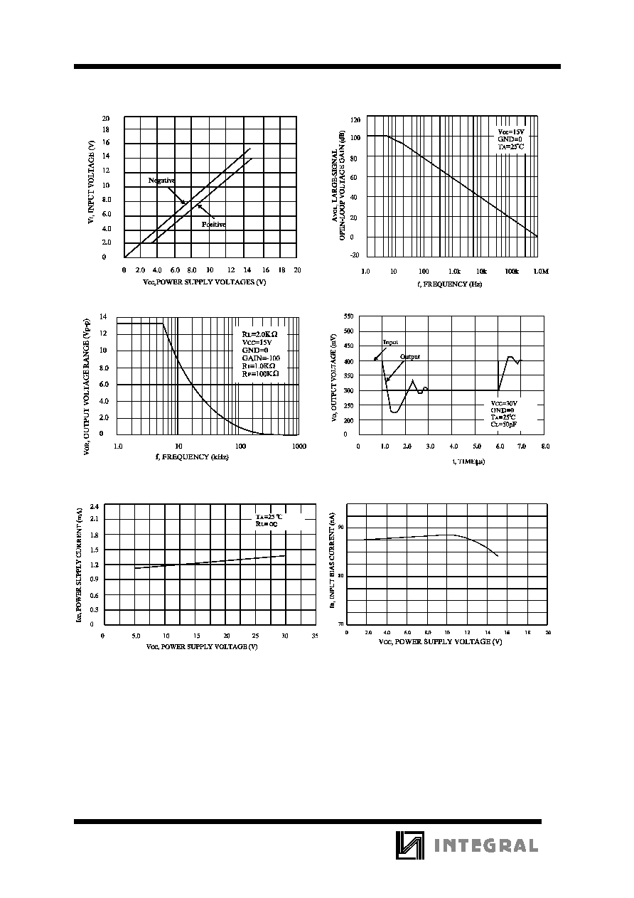
TYPICAL PERFORMANCE CHARACTERISTICS
Figure 1.Input Voltage Range
Figure 2. Open-Loop Frequency
Figure 3. Large-Signal Frequency Response
Figure 4. Small-Signal Voltage Follower Pulse
Response (Noninverting)
Figure 5. Power Supply Current versus Power
Supply Voltage
Figure 6. Input Bias Current versus Power Supply
Voltage