 | –≠–ª–µ–∫—Ç—Ä–æ–Ω–Ω—ã–π –∫–æ–º–ø–æ–Ω–µ–Ω—Ç: IL700D | –°–∫–∞—á–∞—Ç—å:  PDF PDF  ZIP ZIP |
IL700D
Korzhenevskogo 12, Minsk, 220108, Republic of
Belarus
Fax: +375 (17) 278 28 22,
Phone: +375 (17) 278 07 11, 212 24 70, 212 24 61,
212 69 16
E-mail: office@bms.by
URL: www.bms.by
1
H
IGH
V
OLTAGE
H
IGH
-F
REQUENCY
S
TEP
-U
P
S
WITCHING
R
EGULATOR
-C
ONTROLLER
The IL700D is a monolithic high voltage switching regulator-controllers with
PWM/PFM control that is specifically designed to operate from a rectified 220 VAC
line source. This device contain a reference voltage source, oscillation circuit, error
amplifier, phase compensation circuit, PWM control circuit, power supply 450 V
MOS-transistor, 700 V DMOS power switch, and other components. Since the
oscillation frequency is a high 600 kHz, with the addition of a small external
component, the IC can function as switching regulator with high efficiency.
The IL700D provides low-ripple power, high-efficiency, and excellent transient
characteristics thanks to a PWM control circuit capable of varying the duty ratio linearly
from 0% to 82% and optimized error amplifier, and phase compensation circuit.
The IL700D contains a PWM/PFM switching control circuit so that it operates
using PWM control with a duty ratio of 27% or higher and using PFM control with a
duty ratio of lower than 27% to ensure high efficiency in all load ranges.
Pin
No.
Pin Name Function
1 NC
Not
used
2 Vdd
HV
IC high power supply
3 NC
Not
used
4
Vdd
IC internal low power supply
5
Vz
Voltage on zener diode
6
CVREF
Reference voltage source pass
capacitor connection pin
7 GND
Gnd
pin
8
FB
FB for external setting type
9 CSS
Soft-start
capacitor connection pin
10
SENSE
Current limit detection pin
11 NC
Not
used
12 NC
Not
used
13 NC
Not
used
14 NC
Not
used
15
SOURCE Power switch source
16
SOURCE Power switch source
17
SOURCE Power switch source
18 NC
Not
used
19 NC
Not
used
20
DRAIN
Power Switch Drain
IL235Z
Korzhenevskogo 12, Minsk, 220108, Republic of
Belarus
Fax: +375 (17) 278 28 22,
Phone: +375 (17) 278 07 11, 212 24 70, 212 24 61,
212 69 16
E-mail: office@bms.by
URL: www.bms.by
2
Features
û Operate from a rectified 220 VAC line source.
û Oscillation frequency: 600 kHz.
û Output voltage external setting (FB) type available.
FB terminal voltage (V
FB
) 1.0 V.
û Minimum of external components. The only peripheral
components that can be used with IC are a coil, a diode,
capacitors, and a resistor.
û Built-in converter of high voltage in low voltage, using 450 V
MOS-transistor and Zener diode.
û Built-in 700 V DMOS power switch.
û Duty ratio: 0% to 27% typ. PFM control
27% to 82% typ. PWM control
û Built-in current limiting circuit: Assigned by internal resistor (RSENSE).
û Soft-start function: Can be set with an external capacitor (C
SS
).
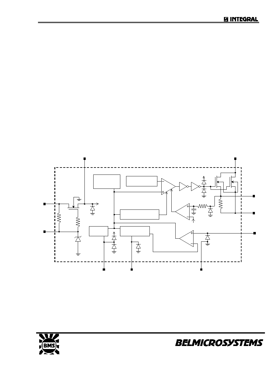
Block diagram
TR2
R1
R2
ZD1
SENSE
Vdd
HV
Vz
Vdd
—SS
—VREF
Vss
FB
DRAIN
Soft-start
circuit
Voltage/current
reference
VREF=1.0V
Rs
Cs
120mV
PWM/PFM switching
control circuit
Phase
compensation
circuit
Triangular wave
oscillation circuit
TR1
SOURCE
RSENSE
* - Pin number are defined during designing
IL700D
Korzhenevskogo 12, Minsk, 220108, Republic of
Belarus
Fax: +375 (17) 278 28 22,
Phone: +375 (17) 278 07 11, 212 24 70, 212 24 61,
212 69 16
E-mail: office@bms.by
URL: www.bms.by
3
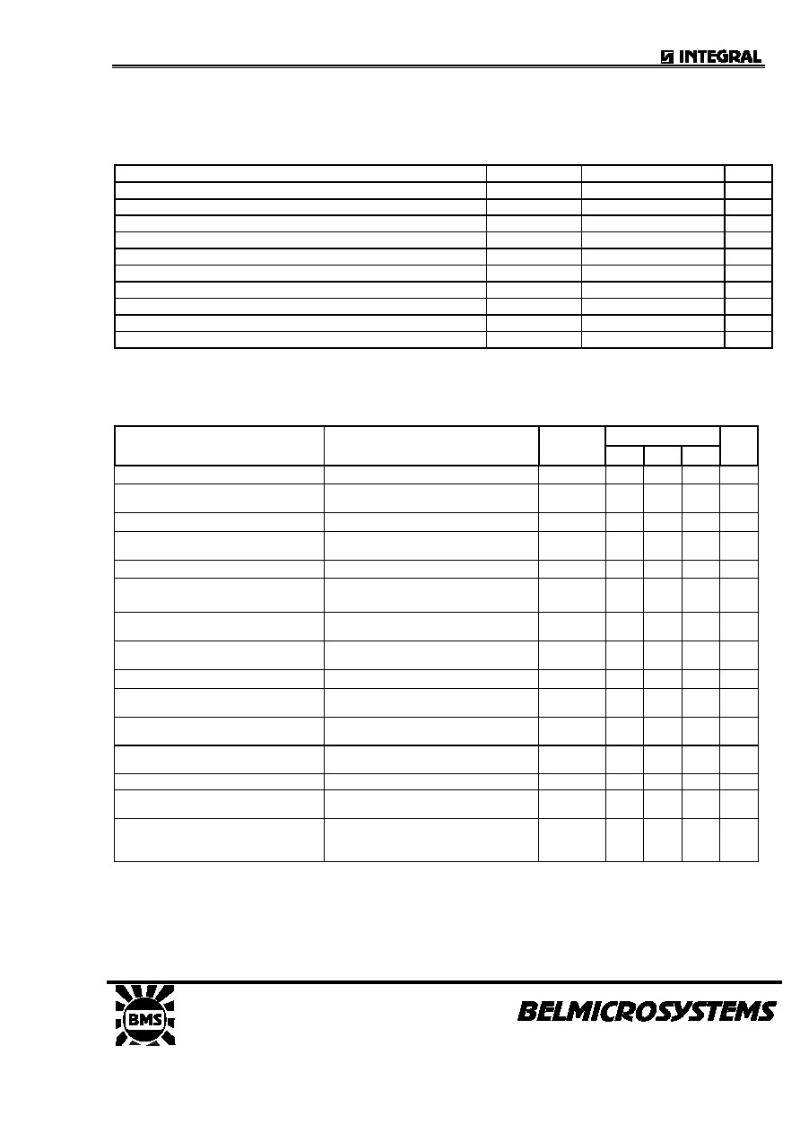
ABSOLUTE MAXIMUM RATING (Ta=25C unless otherwise specified)
Item
Symbol
Ratings
Units
Vdd pin voltage
Vdd
Vss-0.3 to 16
V
Vdd
HV
pin voltage
Vdd
HV
Vss-0.3 to 450
V
DRAIN pin voltage
V
DRAIN
Vss-0.3 to 700
V
DRAIN pin current
I
DRAIN
300
mA
FB pin voltage
V
FB
Vss-0.3 to 16
V
CVREF pin voltage
V
CVREF
Vss-0.3 to Vdd+0.3
V
CSS pin voltage
V
CSS
Vss-0.3 to Vdd+0.3
V
SENSE pin voltage
V
SENSE
Vss-0.3 to Vdd+0.3
V
Vz pin voltage
Vz
Vss-0.3 to Vdd+0.3
V
Power dissipation
P
D
650
mW
ELECTRICAL CHARACTERISTICS (Ta=25C unless otherwise
specified)
Sym-
IL700D
Parameter
Conditions
bol Min
Typ Max Unit
FB pin voltage
Vdd
HV
=220V, Duty=50%, Ta=25
o
C
V
FB
0.98 1.0 1.02
V
FB pin voltage
Vdd
HV
=220V, Duty=50%, Ta= -25
o
C
+85
o
C
V
FB
0.97 1.0 1.03
V
Line regulation
30V ò Vdd
HV
ò 300V, Duty=50%
V
FB1
- - 40
mV
Oscillation start voltage
No external component. The voltage
is applied to Vdd
HV
V
ST
- - 20
V
Current consumption in static mode
Vdd
HV
=220V, V
FB
=1.5V
I
SS1
- -
1
mA
Current consumption in dynamic
mode
Vdd
HV
=220V, V
FB
=0.5V
I
SS2
- -
4
mA
Current limit detection voltage
Judge oscillation stop in "H", at DRAIN
pin, Ta=25
o
C
V
SENSE
90 120
150 mV
Current limit detection voltage
Judge oscillation stop in "H", at DRAIN
pin Ta= -25
o
C +85
o
C
V
SENSE
80 120
160 mV
DRAIN pin output current
Vdd
HV
=220V
I
DRAIN
68 - 172
mA
Oscillation frequency
Vdd
HV
=220V. Measure waveform at
DRAIN pin Ta=25
o
C
f
OSC
510 600
690 kHz
Oscillation frequency
Vdd
HV
=220V. Measure waveform at
DRAIN pin Ta= -25
o
C +85
o
C
f
OSC
500 600
700 kHz
Maximum duty ratio
Vdd
HV
=220V. Measure waveform at
DRAIN pin
MaxDuty 73 82 89 %
PWM/PFM-control switch duty ratio
Vdd
HV
=220V. Under no load
PFMDuty 19 27 35 %
Drain-Source Off-State Leakage
Current
V
DRAIN
=220V
I
DRAIN(off)
- - 50
A
Soft-Start time
Vdd
HV
=220V, C
SS
=4700pF,
I
OUT
=50mA. Measure time until
oscillation occurs at DRAIN pin
T
SS
3.0 -
14.0
ms
IL235Z
Korzhenevskogo 12, Minsk, 220108, Republic of
Belarus
Fax: +375 (17) 278 28 22,
Phone: +375 (17) 278 07 11, 212 24 70, 212 24 61,
212 69 16
E-mail: office@bms.by
URL: www.bms.by
4
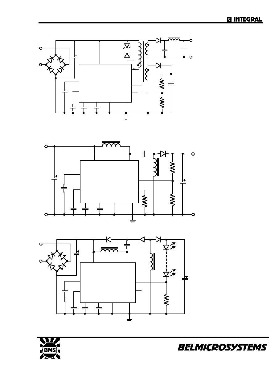
DRAIN
FB
SENSE
SOURCE
Vss
Vdd
HV
CSS CVREF
Vdd
Vz
AC
IN
GND
5V
1A
IL700T
22ÏF
0.1ÏF
10nF 4.7nF 10nF
3.3ÏH
1N4148
3 k
12 k
2.2ÏF
220ÏF
100ÏF
UF1001
MURS160
1N4764
Application Diagram, 85 - 265 VAC Input, 5V/1A Output
Flyback Converter
DRAIN
FB
SENSE
SOURCE
Vss
Vdd
HV
CSS CVREF
Vdd
Vz
Vcc
GND
GND
200mA
5V
IL700T
10ÏF
0.1ÏF
10nF 4.7nF 10nF
330ÏH
0.22ÏF
330ÏH
MURS160
30
12 k
220ÏF
Application Diagram, 100 - 400 VDC Input, 5V/200mA Output SEPIC Converter
DRAIN
FB
SENSE
SOURCE
Vss
Vdd
HV
CSS CVREF
Vdd
Vz
IL700T
0.1ÏF
10nF 4.7nF 10nF
AC
IN
4.7ÏF
10nF
820ÏH
1mH
MURS160
MURS160
MURS160
100
LEDı8
0.1ÏF
Application Diagram, 85 - 265 VAC Input, 1ü100V/10mA Output