 | –≠–ª–µ–∫—Ç—Ä–æ–Ω–Ω—ã–π –∫–æ–º–ø–æ–Ω–µ–Ω—Ç: IL79L24 | –°–∫–∞—á–∞—Ç—å:  PDF PDF  ZIP ZIP |
IL79LXX
1
T
HREE
-T
ERMINAL
L
OW
C
URRENT
P
OSITIVE
V
OLTAGE
R
EGULATORS
The IL79LXX, A Series negative voltage regulators are inexpensive,
easy-to-use devices suitable for numerous applications requiring up to
100 mA. This series features thermal shutdown and current limiting,
making them remarkably rugged. In most applications, no external
components are required for operation.
The IL79LXX devices are useful for on-card regulation or any other
application where a regulated negative voltage at a modest current
level is needed. These regulators offer substantial advantage over the
common resistor/zener diode approach
.
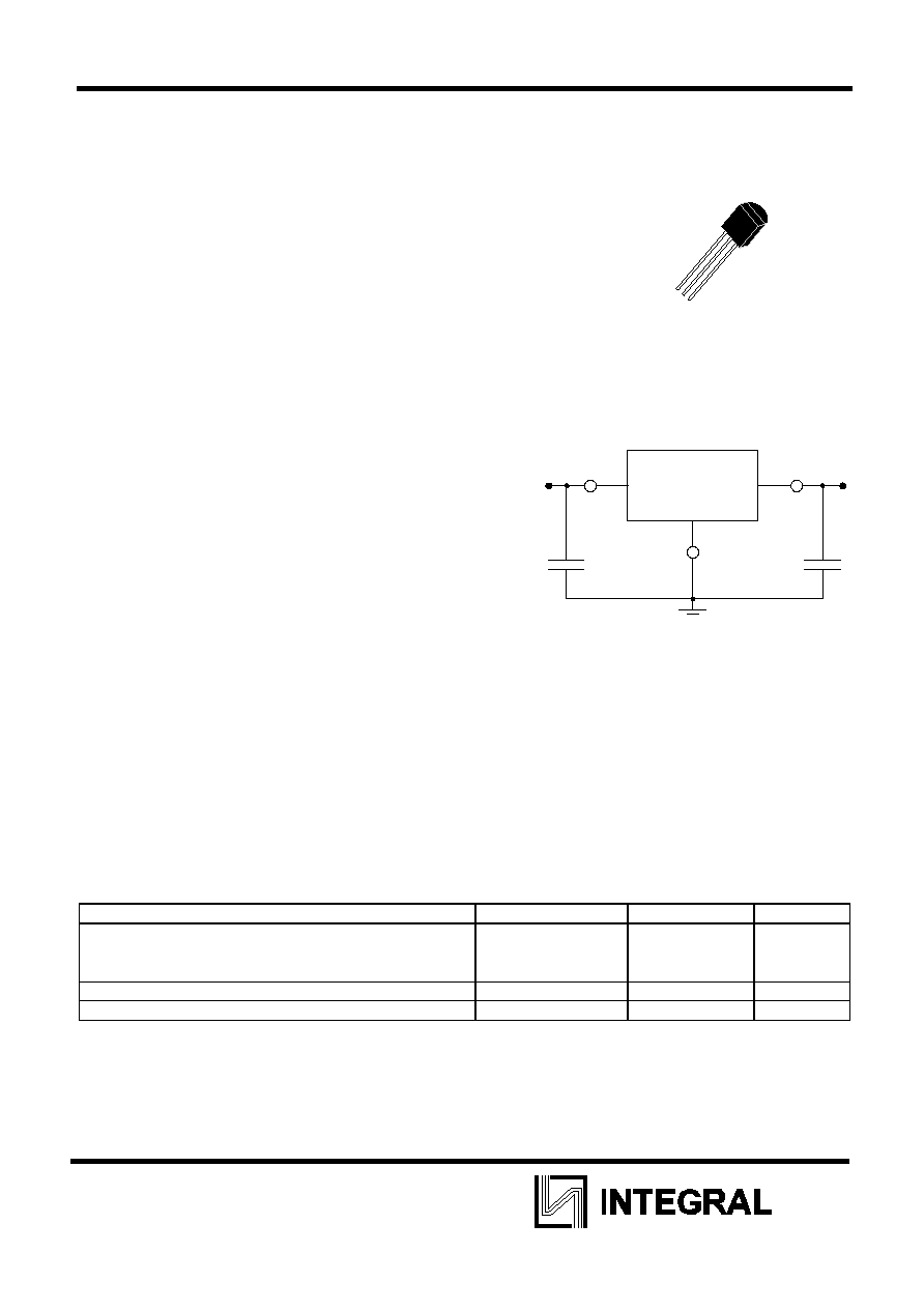
TO-226AA /
TO-92
Pin 1. Output
2.Ground
3.Input
F
EATURES
No External Components Required
û Internal Short Circuit Current Limiting
û Internal Thermal Overload Protection
û Low Cost
û Complementary Positive Regulators
Offered (IL78LXX Series)
û Available in Either 5% (AC) or10% (C) Selections
o
**
0.1
F
in
*
0.33
F
Vout
Vin
I L79LXX
Standard application
A common ground is required between the input
and the output voltages. The input voltage must
remaintypically 2.0 V above the output voltage even
during the low point on the input ripple voltage.
*C in is required if regulator is located an
*
appreciable distance from power supply filter.
**C O is not needed for stability; however, it does
*
improve transient response.
A
BSOLUTE MAXIMUM RATINGS
Rating Symbol
Value
Unit
Input Voltage (-5.0 V)
(-12, -15, -18V)
(-24V)
V
l
-30
-35
-40
Vdc
Storage Temperature Range
Tstg
-65 to +150
úC
Operating Junction Temperature Range
T
J
+150
úC
IL79LXX
2
IL79L05
ELECTRICAL CHARACTERISTICS
(V
l
=-10 V, Io= 40 mA, C
l
= 0.33
F, Co
= 0.1
F, -40úC <
T
J
< +125úC unless otherwise noted.)
Characteristics Symbol
Min
Typ
Max
Unit
Output Voltage (T
J
=+25
úC)
V
O
-4.8
-5.0
-5.2
Vdc
Line Regulation
(T
J
= +25
úC)
-7.0 Vdc
ô Vi ô 20 Vdc
-8.0 Vdc
ô Vi ô20 Vdc
Reg
line
-
-
-
-
150
100
mV
Load Regulation
T
J
= +25
úC, 1.0 mA ò I
O
ò 100 mA) 1.0 mA ò Io
ò 40 mA)
Peg
load
-
-
-
-
60
30
mV
Output Voltage
-7.0 Vdc
ôViô -20Vdc,
(Vi=-10 V, 1.0 mA
òIoò70 mA)
V
O
-4.75
-4.75
-
-
-5.25
-5.25
Vdc
Input Bias Current
(T
J
= +25
úC)
(T
J
=+125
úC)
I
IB
-
-
-
6.0
5.5
mA
Input Bias Current Change
-8.8 Vdc
ôVi ô-20 Vdc)
1.0 mA
òIoò 40 mA
I
IB
-
-
-
-
1.5
0.1
mA
Output Noise Voltage
(T
A
=+25
úC, 10 Hzòfò100 kHz)
Vn -
40
-
V
Ripple Rejection
(-8.0 Vdc
ôVi ô -18 V,
f= 120 Hz, T
J
=
+25
úC)
RR 41
49
-
dB
Dropout Voltage (I
O
=40
mA,
T
J
= +25
úC)
Vi-Vo -
1.7
-
Vdc
IL79L12
ELECTRICAL CHARACTERISTICS
(Vi =-19 V, Io =40 mA, Ci = 0.33
F, Co = 0.1 F, -40úC < T
J
< +125úC, unless otherwise noted.)
Characteristics Symbol
Min
Typ
Max
Unit
Output Voltage (T
J
= +25
úC)
Vo -11.1
-12
-12.9
Vdc
Line Regulation
(T
J
= +25
úC)
-14.5Vdc
ôVi ô 27Vdc
-16 Vdc
ôVi ô 27 Vdc
Reg
line
-
-
-
-
250
200
mV
Load Regulation
T
J
=
+25
úC,
1.0 mA
ò Io
ò 100 mA
1.0
mA
ò Io
ò 40 mA
Peg
load
-
-
-
-
100
50
mV
Output Voltage
-14.5Vdc
ôVi ô-27Vdc, 1.0mAòIoò 40mA) Vi = -
19V, 1.0mA
òIo ò 70mA)
Vo
-10.8 --
10.8
-
-
-13.2
-13.2
Vdc
Input Bias Current
(T
J
= +25
úC)
(T
J
=
+125
úC)
I
IB
-
-
-
-
6.5
6.0
mA
Input Bias Current Change
-16Vdc
ô Vi ô -27Vdc
1.0 mA
ò Io ò 40 mA
I
IB
-
-
-
-
1.5
0.2
mA
Output Noise Voltage
(T
A
= +25
úC, 10Hz ò f ò 100 kHz)
Vn -
80
-
V
Ripple Rejection
-15V
ô Vi ô -25V, f= 120 Hz, T
J
=+25
úC)
RR 36
42
-
dB
Dropout Voltage
(I
O
=
40
mA,
T
J
= +25
úC)
Vi-Vo "
1.7
-
Vdc

IL79LXX
3
IL79L15
ELECTRICAL CHARACTERISTICS
(Vi = -23 V, Io
= 40 mA, Ci = 0.33
F, Co= 0.1 F, -40úC < T
J
< +125úC), unless otherwise noted.)
Characteristics
Symbol Min Typ Max Unit
Output Voltage (T
J
= +25
úC)
Vo -13.8
-15
-16.2
Vdc
Line Regulation
(T
J
= +25
úC, Io
= 40mA)
-30Vdc
òVi ò -17.5Vdc
-30Vdc
ò Vi ò -20Vdc
Reg
line
-
-
-
-
300
250
mV
Load Regulation
(T
J
=
+25
úC,
1.0
mA
ò Io
ò 100 mA)
(T
J
= +25
úC, 1.0 mA ò Io < 40 mA)
Peg
load
-
-
-
-
150
75
mV
Output Voltage
(17.5Vdc
òViò 30Vdc, 1.0 mAòIoò 40 mA) (Vi =
23V, 1.0mA
òIoò 70 mA)
Vo
-13.5
-13.5
-
-
-16.5
-16.5
Vdc
Input Bias Current
(T
J
= +25
úC)
(T
J
=
+125
úC)
I
IB
-
-
-
-
6.5
6.0
mA
Input Bias Current Change
(20Vdc
ò Vi ò 30Vdc)
(1.0mA
ò Io ò 40 mA)
I
IB
-
-
-
-
1.5
0.2
mA
Output Noise Voltage
(T
A
= +25
úC, 10Hz ò f ò 100 kHz)
Vn -
90
-
nV
Ripple Rejection (I
O
= 40 mA, f =120 Hz, 18.5V
ò
Vi
ò 28.5V, T
J
= +25
úC)
RR 33
39
-
dB
Dropout Voltage (T
J
= +25
úC)
Vi-Vo
- 1.7
- Vdc
IL79L18
ELECTRICAL CHARACTERISTICS
(Vi = 27 V, Io
= 40 mA, Ci = 0.33
F, Co = 0.1 F, 40úC < T
J
< +125úC, unless otherwise noted.)
Characteristics
Symbol
Min Typ Max Unit
Output Voltage (T
J
= +25
úC)
V
O
-16.6
-18
-19.4
Vdc
Line Regulation
(T
J
= +25
úC, Io= 40 mA)
-33 Vdc
ò Vi ò -20.7Vdc
-33 Vdc
ò Vi ò -22 Vdc
Reg
line
-
-
-
-
325
275
mV
Load Regulation
(T
J
= +25
úC, 1.0 mA ò Io ò 100 mA)
(T
J
= +25
úC, 1.0 mA ò Io ò 40 mA)
Peg
load
-
-
-
-
170
85
mV
Output Voltage
(-33Vdc
òViò-21.4Vdc, 1.0 mA òIoò 40 mA)
(Vi = -27 V, 1.0mA
òIoò 70 mA)
Vo
-16.2
-16.2
-
-
-19.8
-19.8
Vdc
Input Bias Current
(T
J
=
+25
úC)
(T
J
= +125
úC)
I
IB
-
-
-
-
6.5
6.0
mA
Input Bias Current Change
(-33Vdc
ò Vi ò -22Vdc)
(1.0mA
ò Io ò
40 mA)
I
IB
-
-
-
-
1.5
0.2
mA
Output Noise Voltage
(T
=+25
úC,10Hz ò Io ò 100kHz)
Vn -
150
-
nV
Ripple Rejection
(f = 120 Hz, -33 V
ò Vi ò -23 V, T
J
= +25
úC)
RR 32
46
-
dB
Dropout Voltage (T
J
= +25
úC)
Vi-Vo
- 1.7
- Vdc
IL79LXX
4
IL79L24
ELECTRICAL CHARACTERISTICS
(Vi = 33 V, Io
= 40 mA, Ci = 0.33
F. Co
= 0.1
F,
0úC < T
J
< +125úC, unless otherwise noted.)
Characteristics Symbol
Min
Typ
Max
Unit
Output Voltage (T
J
= +25
úC)
V
O
-22.1
-24
-25.9
Vdc
Line Regulation
(T
J
= +25
úC, Io
= 40 mA)
38 Vdc
òVi ò 27.5 Vdc
38 Vdc
ò Vi ò 28 Vdc
Reg
line
-
-
35
30
350
300
mV
Load Regulation
(T
J
= +25
úC, 1.0 mA ò Io ò 100 mA)
(T
J
= +25
úC, 1.0 mA ò Io ò 40 mA)
Reg
load
-
-
40
20
200
100
mV
Output Voltage
-38Vdc
òViò -28Vdc, 1.0 mA ò Io ò40 mA
Vi= -33Vdc, 1.0 mA
ò Io ò70 mA
V
O
-21.6
-21.6
-
-
-26.4
-26.4
Vdc
Input Bias Current
(T
J
= +25
úC)
(T
J
= +125
úC)
I
IB
-
-
-
-
6.5
6.0
mA
Input Bias Current Change
(-38 Vdc
ò Vi ò -28 Vdc)
(1.0 mA
ò Io ò 40 mA)
I
IB
-
-
-
-
1.5
0.2
rnA
Output Noise Voltage
(T
¿
= +25
úC, 10Hz ò f ò 100 kHz)
Vn -
200
-
nV
Ripple Rejection (I
O
= 40 mA, f= 120 Hz, -
35V
ò Vi ò -29V, T
J
= +25
úC)
RR 30
43
-
dB
Dropout Voltage (T
J
= +25
úC)
Vi-Vo
- 1.7
- Vdc