IL9001
1
DMOS FULL BRIDGE DRIVER
DESCRIPTION
The circuit is a full bridge driver for motor control applications realized
in Multipower-BCD technology which combines isolated DMOS power
transistors with CMOS and Bipolar circuits on the same chip. By
using mixed technology it has been possible to optimize the logic
circuitry and the power stage to achieve the best possible
performance. The DMOS output transistors can operate at supply
voltages up to 42V and efficiently at high switching speeds. All the
logic inputs are TTL, CMOS and
C compatible. Each channel (half-
bridge) of the device is controlled by a separate logic input, while a
common enable controls both channels.
Features
Supply voltage up to 48V
5A max peak current (2A max. for L6201)
Total RMS Current up to 4A;
R
DS
(ON)
0.3 Ohm (typical value at 25
o
C)
Cross conduction protection
TTL Compatible drive
Operating frequency up to 100 kHz
Thermal shutdown
Internal logic supply high efficiency
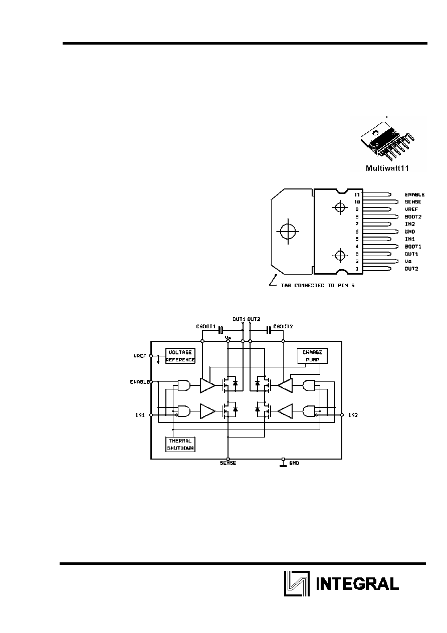
Figure 1. Package and pin connection
Figure 2. Simplified Block Diagram

IL9001
2
PIN FUNCTIONS
Pin Symbols
Functions
1
SENSE 1
Sense resistor to provide the feedback for motor current control of the bridge A
2
IN1
Digital input from the motor controller (bridge A)
3
ENABLE 1
A logic level low on this pin disable the bridge A
4
OUT1
Output of one half bridge of the bridge A
5
GND
Common Power Ground
6
OUT3
Ouput of one half bridge of the bridge �
7
ENABLE 2
A logic level low on this pin disable the bridge �
8
IN 3
Digital input from the motor controller (bridge B)
9
SENSE 2
Sense resistor to provide the feedback for motor current control of the bridge �
10
BOOSTRAP OSC.VCP
Oscillator output for the external charge pump
11
IN 4
Digital input from the motor controller (bridge B)
12
OUT 4
Output of one half bridge of the bridge B
13
Vs2
Supply voltage bridge B
14
Vs1
Supply Voltage bridge A
15
OUT 2
Output of one half bridge of the bridge A
16
IN 2
Digital input from the motor controller (bridge A)
17
VBOOT
Overvoltage input for driving of the upper DMOS
ABSOLUTE MAXIMUM RATING
Symbol Parameter
Test
Conditions
Unit
Vs Supply
Voltage
50
V
V
IM
,
V
EN
Input or Enable Voltage Range
-0.3 to +7
V
Io
Pulsed Output Current
3
A
V
SENSE
Sensing Voltage
-1 to 4
V
V
BOOT
Bootstrap
Supply
60
V
Ptot
Total power dissipation: (Tpins = 80�C)
5
W
Tstg, Tj
Storage and Junction Temperature
-40 to 150
�C
ELECTRICAL CHARACTERISTICS (Vs = 42V, Tj = 25�C unless otherwise specified)
Symbol Parameter
Test
Condition
Min.
���. Max. Unit
Vs Supply
Voltage
12
48
V
Is
Total Quiescent Current
EN1=EN2=H; IN1=IN2=IN3-
IN4=L
10
mA
EN1
=EN2-L
10
mA
fc Commutation
Frequency
20
KHz
T
J
Thermal
Shutdown
150
�C
Td
Dead Time Protection
500
ns
TRANSISTORS
I
DSS
Leakage
Current
OFF
1
mA
R
DS
On
Resistance
ON1
1,2
Ohm
LOGIC LEVELS
V
INL
,
V
ENL
Input Low Voltage
-0.3
0.8
V
V
INH
,
V
ENH
Input High Voltage
2
7
V
I
INL
,
I
ENL
Input Low Current
IN1 = IN2 = INS = IN4 - EN1 =
EN2 = L
-10
u�
I
INH
,
I
ENH
Input High Current
IN1 = IN2 = INS = IN4 = EN1 =
EN2 = H
50
u�
IL9001
3
ELECTRICAL CHARACTERISTICS (Continued) LOGIC CONTROL TO POWER DRIVE TIMING
Symbol Parameter
Test
Conditions
Min. Typ.
Max.
Unit
t
1
(Vi)
Source Current Turn-off Delay
300
ns
t
2
(Vi)
Source Current Fall Time
200
ns
t
3
(Vi)
Source Current Turn-on Delay
400
ns
t
4
(Vi)
Source Current Rise Time
200
ns
t
5
(Vi)
Sink Current Turn-off Delay
300
ns
t
6
(Vi)
Sink Current Fall Time
200
ns
t
7
(Vi)
Sink Current Turn-on Delay
400
ns
t
8
(Vi)
Sink Current Rise Time
200
ns
(*) Limited by power dissipation
(**) In synchronous rectification the drain-source voltage drop VDS is shown in fig. 4 (L6202/03);
typical value for the L6201 is of 0.3V.
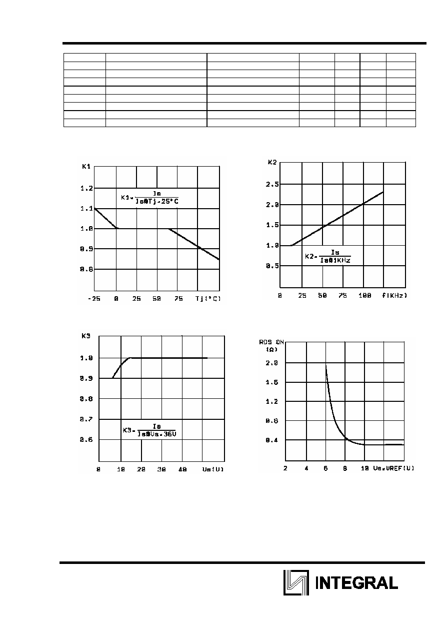
Figure 1: Typical Normalized I
S
vs. T
j
Figure 2: Typical Normalized Quiescent Current vs.
Frequency
Figure 3: Typical Normalized I
S
vs. V
S
Figure 4: Typical R
DS(ON)
vs. V
S
~ V
ref
IL9001
4
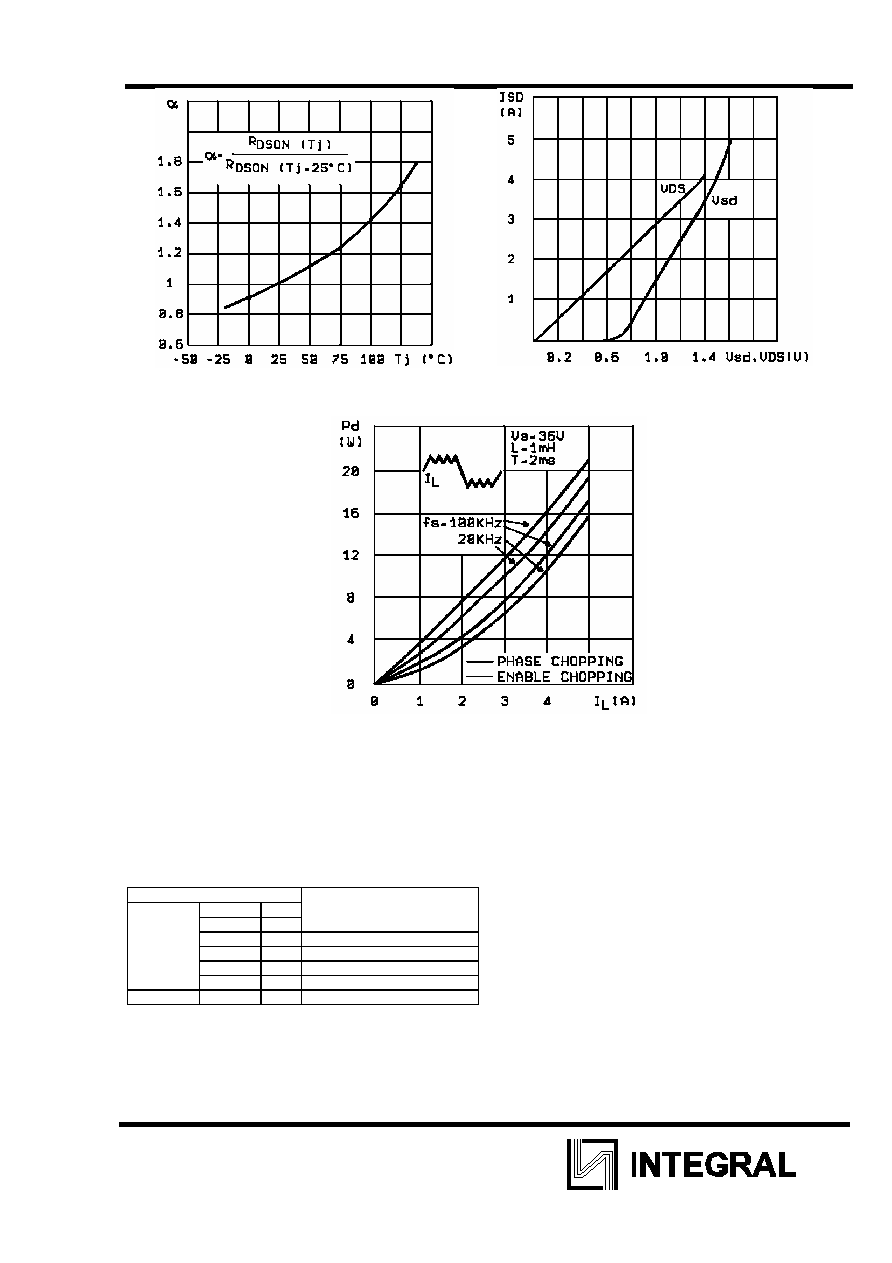
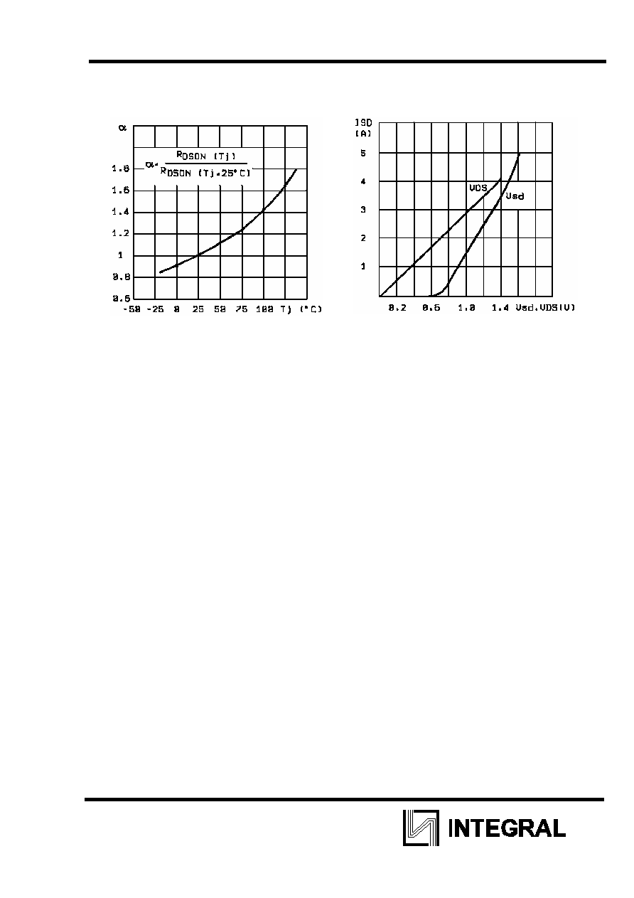
Figure 5: Normalized R
DS(ON)
at 25
o
C vs. Temperature
Typical Values
Figure 6b: Typical Diode Behaviour in Synchronous
Rectification
Figure 7b: Typical Power Dissipation vs I
L
CIRCUIT DESCRIPTION
The IL9001 is a monolithic full bridge switching motor driver realized in the new Mul-tipower-BCD technology
which allows the integration of multiple, isolated DMOS power transistors plus mixed CMOS/bipolar control
circuits. In this way it has been possible to make all the control inputs TTL, CMOS and C compatible and
eliminate the necessity of external MOS drive components. The Logic Drive is shown in table 1.
Table 1
Inputs
IN1 IN2
Output Mosfets (*)
L
L
Sink 1, Sink 2
L
H
Sink 1, Source 2
H
L
Source 1, Sink 2
V
EN
= H
H
H
Source 1, Source 2
V
EN
= L
X
X
All transistors turned oFF
L = Low
H = High X = DON't care
(*) Numbers referred to INPUT1 or INPUT2 controlled output stages
Although the device guarantees the absence of cross-conduction, the presence of the intrinsic
diodes in the POWER DMOS structure causes the generation of current spikes on the sensing
terminals. This is due to charge-discharge phenomena in the capacitors C1 & C2 associated with
IL9001
5
the drain source junctions (fig. 14). When the output switches from high to low, a current spike is
generated associated with the capacitor C1. On the low-to-high transition a spike of the same
polarity is generated by C2, preceded by a spike of the opposite polarity due to the charging of the
input capacity of the lower POWER DMOS transistor (fig. 15).
Figure 14: Intrinsic Structures in the POWER
DMOS Transistors
Figure 15: Current Typical Spikes on the Sensing
Pin
TRANSISTOR OPERATION
ON State
When one of the POWER DMOS transistor is ON it can be considered as a resistor RDS (ON)
throughout the recommended operating range. In this condition the dissipated power is given by :
PON = RDS (ON) IDS
2
(RMS)
The low RDS (ON) of the Multipower-BCD process can provide high currents with low power
dissipation.
OFF State
When one of the POWER DMOS transistor is
OFF the V
DS
voltage is equal to the supply volt-
age and only the leakage current IDSS flows. The power dissipation during this period is given by :
POFF = VS IDSS
The power dissipation is very low and is negligible in comparison to that dissipated in the ON
STATE.
Transitions
As already seen above the transistors have an intrinsic diode between their source and drain that
can operate as a fast freewheeling diode in switched mode applications. During recirculation with
the ENABLE input high, the voltage drop across the transistor is RDS (ON) ID and when it
reaches the diode forward voltage it is clamped. When the ENABLE input is low, the POWER MOS
is OFF and the diode carries all of the recirculation current. The power dissipated in the transitional
times in the cycle depends upon the voltage-current waveforms and in the driving mode. (see Fig.
7ab and Fig. 8abc).
Ptrans. = IDS (t) VDS (t)