ILA1238NS
1
AM/FM
M
ONO
R
ECEIVER
ILA1238NS (analog of CXA1238S, SONY) - high-quality one-chip
stereoreceiver designed for receipt of AM/FM signals of broadcasting
stations. The receiver contains: high-frequency amplifiers and AM and FM
mixers, AM and FM intermediate frequency amplifiers, AM and FM
detectors, output decoder of stereosignal for coding system with pilot tone.
û Low consumption current (in FM mode Icc=12.5 mA, in ¿Ã mode Icc=9.5
mA at Ucc=6 V)
û LED indication of tuning
û LED indication of "STEREO" mode
û Switching-off noiseless FM tuning
û Small number of peripheral components
PACKAGE
30-pin mini-DIP
T
A
= -10
ú...+70ú C
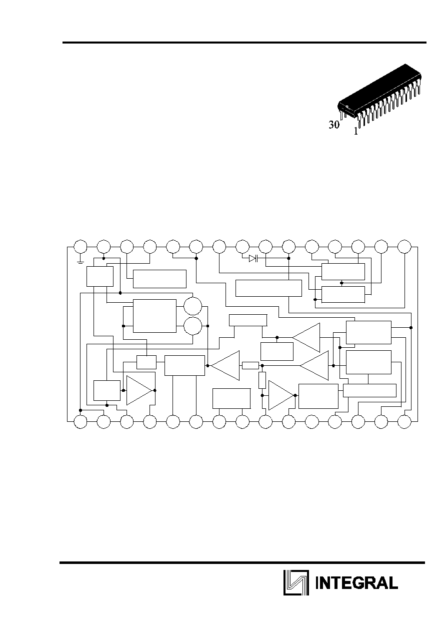
BLOCK DIAGRAM
DISCRI
VCO
REGULATOR
MULTIPLEX
COUNTER
1/2
PD2
PD1
SW
M/ST
AMP
DECODE
MUTING
BLEND
AUTO
FILTER
RIPPLE
BU
BU
AMP
AMP
AMP
AMP
AMP
DC
DC
DC
TUNING IND
CONTROL
MUTING
DETUNE
AM IF
DET
FM IF
REGULATOR
AM FE
FM FE
29
28
27
26
25
24
23
22
21
20
19
18
17
16
15
14
13
12
11
10
9
8
7
6
5
4
3
2
1
30
Note:
VCO - voltage controlled oscillator,
REGULATOR - reference voltage source,
MULTIPLEX REGULATOR - reference voltage source for stereodecoder,
FM FE - heterodyne oscillator, high frequency amplifier and FM path mixer,
AM FE - heterodyne oscillator, high frequency amplifier and AM path mixer,
FM IF DISCRI - intermediate frequency amplifier and FM path demodulator,
AM IF DET - intermediate frequency amplifier and AM path detector ,
TUNING IND - tuning indicator driver,
DETUNE MUTING CONTROL - muting control block,
DC AMP - DC amplifier,
BU AMP - buffer amplifier,
M/ST SW - "MONO"-"STEREO" switch,
DECODE AMP - decoder and LF signal amplifier,

ILA1238NS
2
RIPPLE FILTER - internal stress source with ripple filter,
1/2 COUNTER - VCO frequency devider,
PD1,PD2 - phase detectors of VCO frequency tuning
AUTO BLEND - signal level block for VCO frequency tuning,
MUTING - "MONO" and "STEREO" modes control block.
ABSOLUTE MAXIMUM RATINGS
Symbol Parameter Value
Unit
Ucc Supply
voltage
10
V
Topr
Operation temperature
-10 ... +70
úC
Tstg
Storage temperature
-55 ... +150
úC
Tjmax
Junction maximum temperature
125
úC
Pd
Allowable power dissipation
500
mW
RECOMMENDED OPERATION CONDITIONS
Symbol Parameter Value
Unit
Ucc
Supply voltage
2.0 ... 9.0
V
PINS DESCRIPTION
Voltage, V
Equivalent electrical circuit
Description
Symbol Ucc=3V Ucc=6V
FM ¿Ã FM ¿Ã
1
29
PLL LPF1
PLL LPF2
0.86
0.86
0.86
0.86
0.86
0.86
0.86
0.86
26K
26K
MPX REG
29
1
Low frequency
filter for VCO
phase selftuning
circuit
2
3
PILOT DET
LPF1
ø
PILOT DET
LPF2
0.95
0.95
0.95
0.95
0.95
0.95
0.95
0.95
2
3
Pins for
connecting
capacitance of
low frequency
filter of pilot tone
detector
4
ST IND
VCO CHECK
1.6
1.6
4.5
4.5
VCO
MPX REG
13K
4
Pin of indicator of
"STEREO" mode
and frequency
control 76 kHz


