ILA8362W
1
S
INGLE
-
CHIP
TV
PROCESSOR
IC
FOR VISION AND SOUND
IF
PROCESSING
,
VIDEO AND SYNCHRONIZATION FOR B
/
W
TV
IC DESCRIPTION
ILA8362W is intended for b/w TV receiver and contain functional units for video and
sound IF signals, line and frame synchronization , output Y-signal.
IC FEATURES
û circuit for processing Vision IF (positive and negative modulation).
û FM sound demodulator (4.5-6.5 ÃHz).
û Addition inputs for A/V (external and internal video inputs, internal and external audio inputs).
û Embedded delay line for brightness signal.
û control IC for output Y-signal and external Y-input and possibility of a direct information display on screen
(OSD
û mode).
û Line synchronisation with two control circuits and a generator (adjustment is not needed).
û IC for frame divider and preamplifier of frame scanning.
û Low power consumption (500 mW).
û Minimum quantity of external parts.
û Only one adjustment is required (IF demodulator).
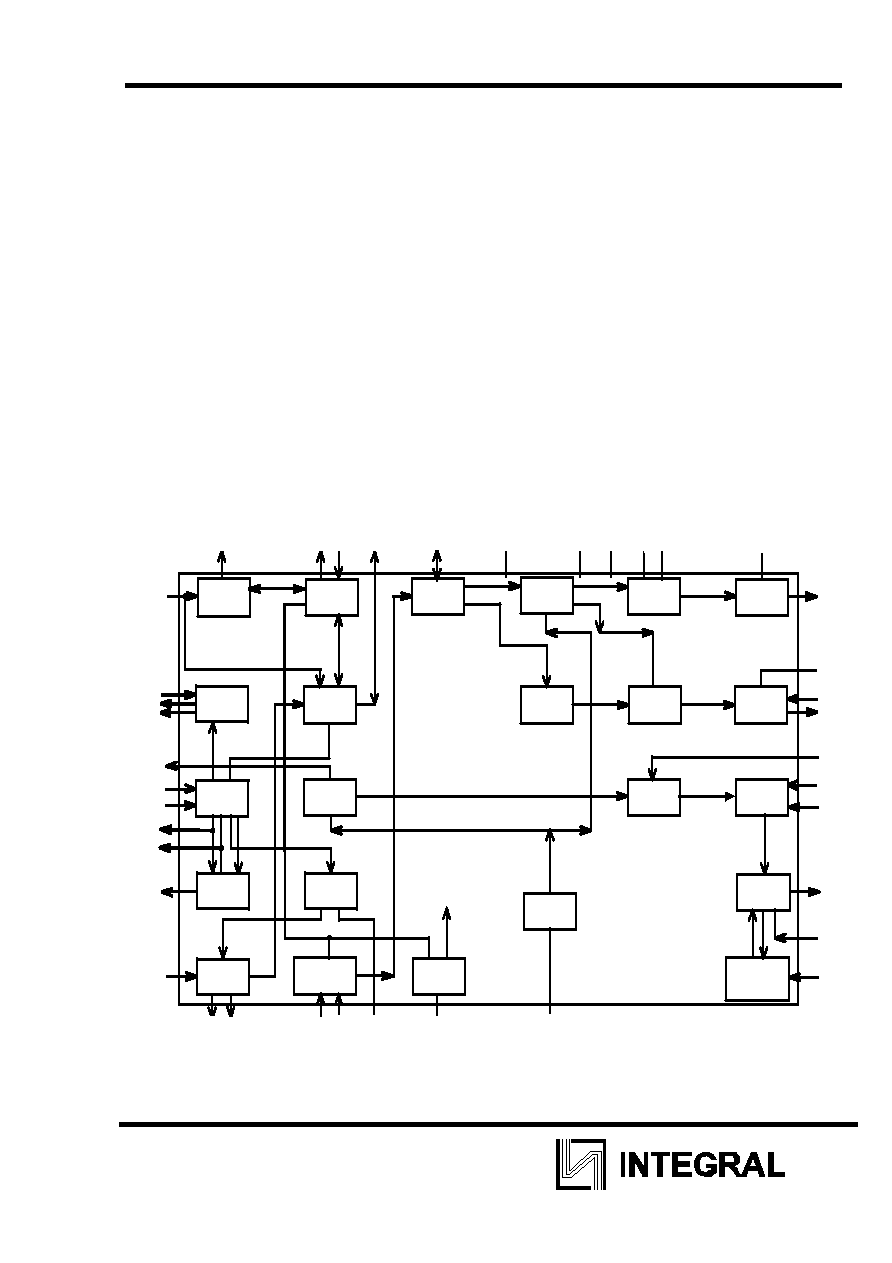
Block diagram of TV signal processor ILA 8362 W
¬€’ŒƒÕŒ… Y
¿— ¿ƒ
SOUND
PREAMPL.
VOLUME
COMTROL
SOUND SWITCH
SYNC
SEPARATOR
PHASE 1 DET.
LINE
GENERATOR
AGC
AGC TUNER
lINE SCANNING
OUTPUT
PHASE 2 DET.
HORIZ. SHIFT
SOUND LIMITER
DEMODULATOR
FRAME SYNCH
SEPARATOR
FRAME DIVIDER
CIRCUIT
IFAMPLIF.
DEMODULATOR
FILTOR TUNING
CIRCUIT
—’≈ÿ
–≈√”À»–Œ¬- »
◊®“ Œ—“»
Y-¬’Œƒ€
—’≈ÿ
ŒÃÔ“¿÷»»
VIDEO
AMPLIFIER
PAFTC
CIRCUIT
VIDEO IDENTIF.
CIRCUIT
VIDEO SIGNAL
SWITCHING CIRCUIT
QWARZ
GENERATOR
INPUT SWITCH
LIMITER OF WHITE
CONTRAST
ADGUSTMENT
fRAME
SCANNING
OUTPUT
50
51
6
1
1
39 38
36
37
43
14
21
17
18
40
44
33
16
7
13
15
52
8
4
9
3
46
45
12
48
47
49
5
35
2
32
42
11
10
41
ILA8362W incorporate advantages of bipolar and MOS technologies, fulfill almost
all low signal functions of w/b TV receiver. To assemble b/w TV-set it's necessary to add
tuner, output stages for video, audio, frame and line scannig.
ILA8362W
3
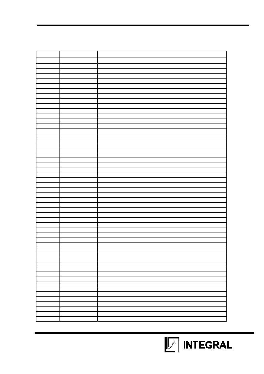
PIN DESCRIPTION TABLE
Pin description table for single-chip TV processor IC for vision and sound
IF processing,
video and synchronization for b/w TV
pin No
Symbol
Description
1 2
3
01
AUDEEM
Sound distortion correction
02
IFDEM1
connection of IF demodulator filter
03
IFDEM2
connection of IF demodulator filter
04 IDENT
Videoidentification
output
05
SOIF
IF sound and volume control input
06
EXTAU
external sound input
07 IFVO
Video
output
08
DECdig
Digital supply decoupling
09 AFCOUT
AFC
output
10 Vcc
Supply
11 OV1
Ground
1
12 DECft
Filter
decoupling
13
CVBSint
Internal video imput
14
PEAK
Sharpness control input
15
CVBSext
External video input
16
VCH
Video switch input
17
BRI
Brightness control input
18
YO
Y output
19 unused
20 unused
21
YINCH
Y input switch input
22 unused
23 unused
24 unused
25 unused
26 unused
27 unused
28 unused
29 unused
30 unused
31 unused
32
YIN
External Y input
33
CON
Contrast control input
34 unused
35
XTAL
Quartz connection (4.43 ÃHz)
36
HOSC
Line scanning generator starting
37
HOUT
line scanning output
38
FBI/SCO
Reverse motion signal input, three level pulse output
39 PH2LF
‘2 detector loop filter
40 PH1LF
‘1 detector loop filter
41 OV2
Ground
2
42
VFB
frame scanning loop input
43
VRAMP
frame scanning generator input
44
VOUT
frame scanning output
45
IFIN1
IF input 1
46
IFIN2
IF input 2
47
AGCOUT
External AGC output
48
DECagc
AGC capacity connection
49
TUNEadj
external AGC threshold adjustment input
50 AUOUT
Sound
output
51 DECdem
Sound
demodulator capacity connection
52
DECbg
Analog decoupling supply
ILA8362W
4
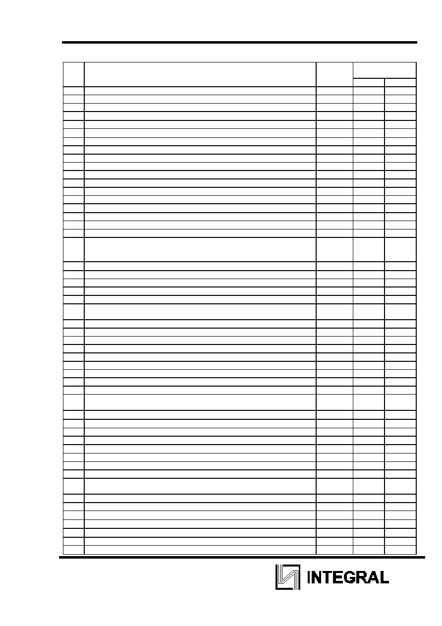
MAIN ELECTRIC PARAMETERS FOR ILA8362W
Target
N
Parameter
Symbol
Min Max
1 2
3
4
5
1. Supply
current,
Ï¿ Ip
___
100
2.
Scanning starting threshold, V
Uth
5.8
6.8
3.
Video IF amplifier input sensitivity , RMS value,
V
Ui(rms) ___ 100
4.
Gain control range ¿GC, dB
Gcr
64
___
5.
AGC efficiency (while input signal changing is 50dB), dB
___ 6
6.
White level on videoamplifier output for negative modulation signal, V
Uw7
3.4
5.1
7.
Synchrosignal upper level on videoamplifier output , V
Us7
1.5
2.5
8. Videoamplifier
output resistance, Œhm R
07
___ 50
9.
Signal altitude on videoamplifier output for negative modulation signals, V
U
0p-p
1.6 2.8
10. Videosignal non-linearity on videoamplifier output, %
NLvid
___
9
11. Max white level on on output of V-ampl.,V
Uth
4,0
5.6
12. Signal/noise ratio on V-ampl. output while input signal altitude is 10mV, dB
S/N
52
___
13. Saturation voltage on external AGC, mV
U
MAX
300
14. Input signal variation causing whole change of AGC voltage, dB
U47
0.5 4
15. Control
voltages
range, V
Ucr
0.5
4.5
16. Voltage swing on AFC output , V
U
5.8
___
17. Characteristic's
slope,
Hz fsl
120
200
18. Output voltage on identification output
when there is no signal , V
with signal, V
Uo
___
7,0
0.5
19. Voltage on identification output while feeding input IF with altitude 100
V, V
Uid
7.0
20. Input sensitivity, RMS value, mV
2
21. Rejection of amplitude-modulated signal , dB
AMR
46
___
22.
23. Output resistance, kŒhm R
01
12 18
24. Output signal altitude variation in PAFTC capture range of sound
demodulator, dB
≈Ó 3
25. Constant component of output voltage , V
U1
2.5
3.5
1 2
3
4
5
26. Output voltage altitude, RMS value, mV, (pin 1)
Uorms
250
400
27. Output signal altitude at level 6dB, RMS value, mV, (pit 50)
Uorms
400
800
28. Constant component of output voltage, V
U50
2.5
3.7
29. Non-linear distortion ratio, %
THD
___
0.6
30. Ratio signal/noise for internal signal source, dB
S/N
60
___
31. Adjustment
range, dB
VOLcr
80
___
32. Output signal rejection within silence mode, dB
OSS
80
___
33. Output signal's constant component bias while transition into silence mode,
mV
U50
___ 100
34. External signal gain, dB¡
Gv
7 13
35. External and internal signals inter-penetration under max gain, dB
60 ___
36. rejection of input videosignal not being selected, dB
ISS
50
___
37. Black level differentiation between internal and external signals, mV
Udiff
___
100
38. Input currents ,
¿
Ii
0.13
39. Input current, m¿ I21
___
0.2
40. Internal Y-signal rejection, dB
SSint
46
___
41. External Y-signal rejection, dB
SSext
46
___
42. Y-signal rejection in mode of OSD signal connection directly to Y output ,
dB
SSbt 46
43. Input current in synchronization absence , mA
I
14
0.5
1.3
44. Generator free oscillations frequency , Hz
ffr
15156
16094
45. Max frequency deviation while starting line scanning, %
fmax
___ +75
46. PAFTC holding band , Hz fHR
___
1.2
47. PAFTC capture band, Hz fCR
___
0.6
48. Low level of output voltage, V
Uol
___
0.3
49. Max output current, m¿ Imax
10

ILA8362W
5
Target
N
Parameter
Symbol
Min Max
1 2
3
4
5
50. Constant voltage on line scanning output under operation of protection
against X-ray, V
Uop 6.5
51. Fulfillment ratio , %
n
43
57
52
Input voltage while reverse moving, V
Uicl
2.2
3.8
53. Output voltage of
strobe , V
suppression level, V
Uo
4.3
1.3
6.3
2.2
54. Width
of
strobe pulse,
s
field, line suppression,
tW
3.2
14
4.1
14
55. Ramp voltage altitude (swing), V
Usaw
1.3
1.7
56. Max output voltage, V
Uomax
4.0
___
57. Min output voltage, V
Uomin
___
0.3
58. Constant voltage on frame scanning output while pin 42 protection is
operating for
lower threshold, V
upper threshold, V
Uop
4.0
0.3
59. Internal bias current of output emitter follower , m¿ Ib
0.1
60. Input current,
¿
I
42
15
61. Control range of contrast scale, dB
CRc
17
29
62. Brightness control range, V
—Rb
0.6
1.4
63. Output signal altitude at nominal contrast range, swing,V Uo
2.7
4.5
64. Suppression level on Y-output, V
Uobl
0.6
0.9
65. Black level on Y-output, V
Uobk
1.0
1.6
66. Max pick level of white, V
Umax
3.8
6.5
67. Internal bias current of output emitter follower, m¿ Ib
1.8
68. Max current source , m¿ Is
5
LIMITING OPERATION CONDITIONS
Values of limiting electrical operation conditions are given in temperature range
from -60ú— to +85ú— .
Parameter name , measurement unit
Symbol
Limiting conditions
Min
Max
Supply voltage, V
Up
7.2
8.8
Range of control voltage on pins 05,17,25,26,27, V
Ui
0
5.0
