IN145403
IN145404
IN145405
IN145408
1
D
RIVERS
/R
ECEIVERS
RS-232-E
These devices are silicon gate CMOS ICs that combine both the transmitter and receiver to fulfill the
electrical specifications of EIA Standard 232-E and CCITT V.28. The drivers feature true TTL input
compatibility, slew rate limiting outputs, 300 a power-off source impedance, and output typically
switching to within 25% of the supply rails. The receivers can handle up to 25V while presenting 3 to
7 kn impedance. Hysteresis in the receivers aid in the reception of noisy signals. By combining both
drivers and receivers in a single CMOS chip, these devices provide efficient, low-power solutions for
both EIA-232-E and V.28 applications. These devices offer the following performance features:
D
RIVERS
� 5 to 12 V Supply Range
� 300 Q Power-Off Source Impedance
� Output Current Limiting
� TTL and CMOS Compatible Inputs
�
Driver Slew Rate Range Limited to 30 V/
s
Maximum
R
ECEIVERS
� 25V Input Range
� 3 to 7 kn Input Impedance
� 0.8V of Hysteresis for Enhanced Noise Immunity
� TTL and CMOS Compatible Outputs
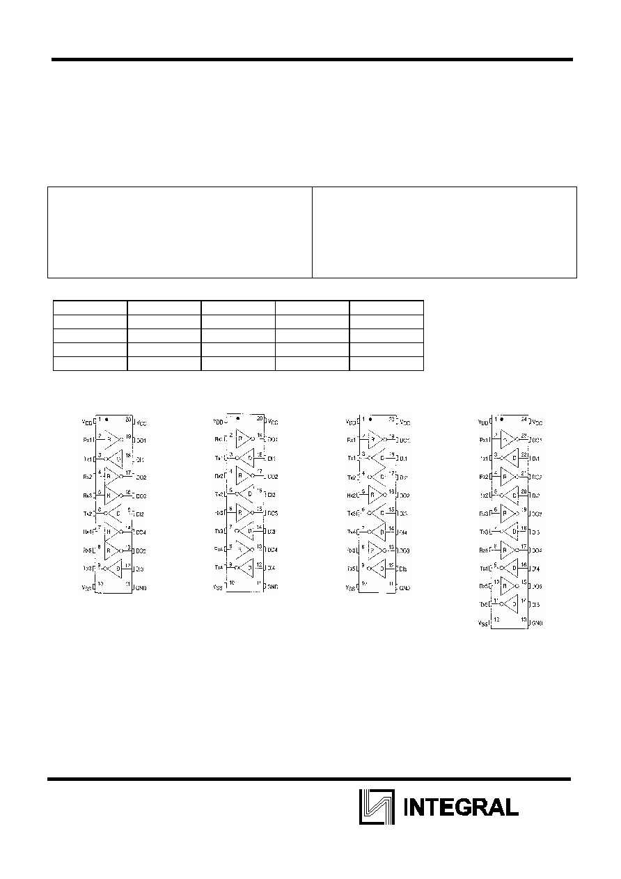
� Available Driver/Receiver Combinations
Device
Drivers
Receivers
Figure
No. ot Pins
IN145403 3
5
1
20
IN145404 4
4
2
20
IN145405 5
3
3
20
IN145408 5
5
4
24
IN145403 IN145404 IN145405 IN145408
3 DRIVERS/5 RECEIVERS
4 DRIVERS/4 RECEIVERS
5 DRIVERS/3 RECEIVERS
5 DRIVERS/5 RECEIVERS
IN145403
IN145404
IN145405
IN145408
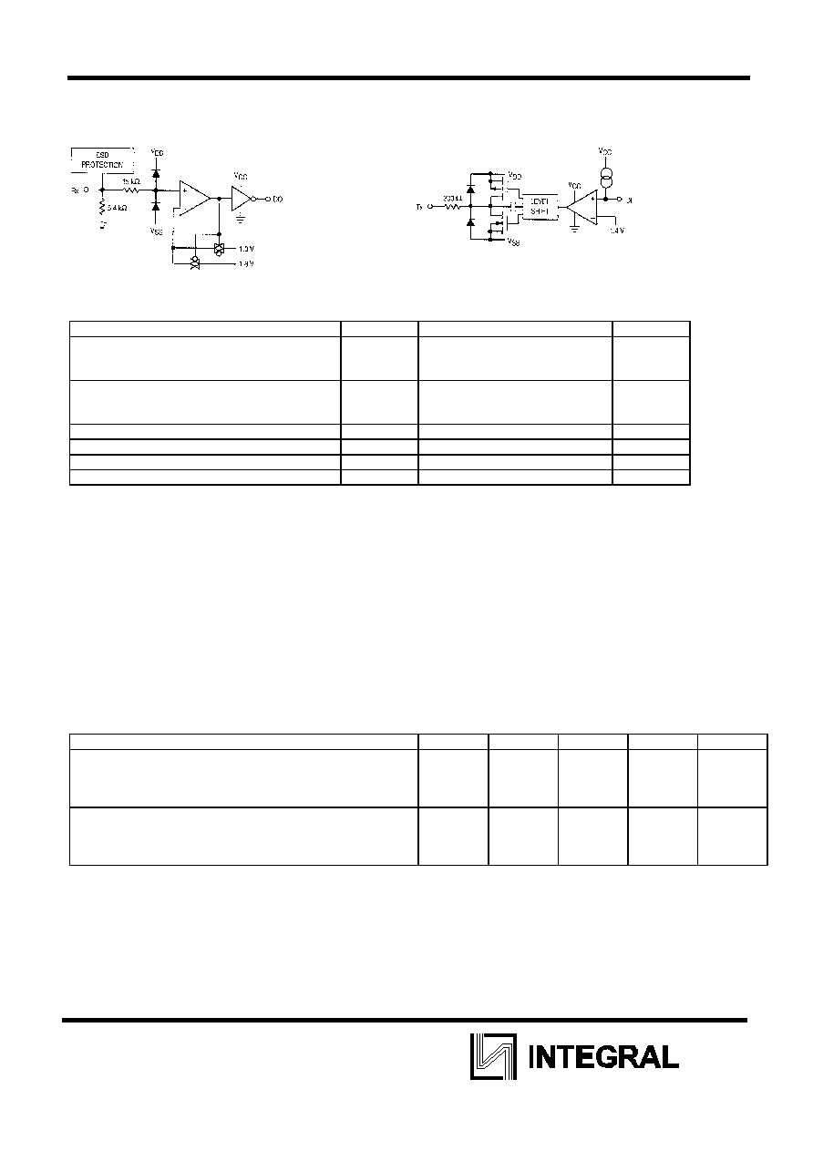
2
FUNCTIONAL DIAGRAM
R
ECEIVER
D
RIVER
ABSOLUTE
MAXIMUM
RATINGS
(Voltages referenced to GND, except where noted)
Rating Symbol
Value
Unit
DC Supply Voltage (V
DD
�V
CC
)
V
DD
V
SS
V
CC
-0.5 to+13.5
+0.5 to -13.5
- 0.5 to + 6.0
V
Input Voltage Range
Rx1 - Rxn
DI1 -DIn
V
IR
Vgg-15
lo
VDO
+ 15 0.5toVcc+15
V
DC Current Drain per Pin
I
00
mA
Power Dissipation
P
D
1
W
Operating Temperature Range
TA
-4010+85
�C
Storage Temperature Range
Tstg
-8510+150
�C
This device contains circuitry lo protect the inputs and outputs against damage due to high static voltages or electric fields:
however, it is advised that normal precautions be taken to avoid applications ol any voltage higher than maximurn rated
voltages to this high impedance circuit.
For proper operation it is recommended that V
out
and V
in
be constrained to the ranges described as follows: Digital I/O:
Driver Inputs (Dl):
(GND
�V
DI
�V
CC
)
Receiver Outputs (DO):
(GND
�V
DO
�V
CC
)
EIA-232 I/O: Driver Outputs (Tx):
(V
SS
�V
Txl-Txn
�V
DD
)
Receiver Inputs (Rx):
V
SS
-15V
�V
RxI-Rxn
�V
DD
+15 V
Reliability of operation is enhanced if unused outputs are tied off to an appropriate logic voltage level (e.g., either GND or
V
CC
for DI, and GND for Rx).
DC ELECTRICAL CHARACTERISTICS (All polarities referenced to GND=0V, T
A
=-40 to +85�C)
Parameter Symbol
Min
Typ
Max
Unit
DC Supply Voltage
V
DD
V
SS
V
CC
4.5
-4.5
4.5
5 to 12
-5 to-12
5
13.2
-13.2
5.5
V
Quiescent Supply Current (Outputs Unloaded, Inputs Low)
V
DD
=+12V
V
SS
= -12V
V
CC
=+5V
I
DD
I
SS
I
CC
-
-
-
425
-400
110
635
-600
200
nA

IN145403
IN145404
IN145405
IN145408
3
RECEIVER ELECTRICAL SPECIFICATIONS (Voltage polarities referenced to GND=0V,
V
DD
=+12V, V
SS
=-12 V, T
A
=-40 to+85�C, V
CC
=+5 V10%)
Characteristic Symbol
Min
Typ
Max
Untt
Input Turn-On Threshold Rxl - Rxn V
DD
=V
OL
V
on
1.35 1.8 2.35 V
Input Tum-Ofl Threshold Rxl - Rxn V
DD
=V
OH
V
off
0.75 1 1.25 V
Input Threshold Hysteresis
=Von-Voff
V
hys
0.6 0.8 -- V
Input Resistance
(Vss-15V)
�V Rx1 -Rxn�(V
DD
+15V)
R
in
3 5.4 7 k
High Level Output Voltage I
out
=-20
A
V
Rx
=-3 to -25V * (D01-D0n) I
out
=-1.0mA
V
OH
4.9
3.8
4.9
4.3
-
-
V
Low Level Output Voltage I
out
=+2mA
V
R
X
=+3 to+25V (D01 - D0n) I
out
= +4 mA
V
OL
-
-
0.02
0.5
0.5
0.7
V
* This is the range of input voltages as specified by EIA-232-E to cause a receiver to be in the high or low.
DRIVER ELECTRICAL SPECIFICATIONS (Voltage Polarities Referenced to GND =0V, V
DD
=+12V,
V
SS
=-12V, T
A
=-40 to +85�C,V
CC
=+5V 10%)
Characteristic Symbol
Min
Typ
Max
Unit
Digital InputVoltage DII-DIn
Logic 0
Logic 1
V
IL
V
IH
-
2
-
-
0.8
-
V
Input Current DIl - DIn
V
DI
=GND
V
DI
=V
CC
I
IL
I
IH
-
-
7
-
-
1.0
nA
Output High Vollage Txl-Txn
V
DI
=Logic 0. R
L
= 3k
V
DD
=+5.0V, V
SS
=-5.0V
V
DD
=+6.0V, V
SS
=-6.0V
V
DD
=+12.0V, V
SS
=-12.0V
V
OH
3.5
4.3
9.2
3.9
4.7
9.5
-
-
-
V
Output Low Voltage* Txl - Txn
V
DI
= Logic 1, R
L
= 3 k
V
DD
=+5.0 V, V
SS
=-5.0V
V
DD
=+6.0 V, V
SS
=-6.0V
V
DD
=+12.0 V, V
SS
=-12.0V
V
OL
-4
-4.5
-10
-4.3
-5.2
-10.3
-
-
-
V
Output Short Circuit Current Txl-Txn
V
DD
=+12 V, V
SS
=-12V
Tx Shorted to GND
Tx Shorted to 15V
I
SC
-
22 60
60 100
mA
'* Voltage specifications are in terms of absolute values.
SWITCHING CHARACTERISTICS (V
CC
=+5V 10%, V
DD
=+12V, V
SS
=-12V, T
A
=-40 to+ 85�C; See
Figures 2 and 3)
Characteristic Symbol
Min
Typ
Max
Unit
Drivers
Propagation Delay Time Tx
Low-to-High R
L
=3k
, C
L
= 50 pF
t
PLH
-
500
1000
ns
High-to-Low R
L
=3 k
, C
L
=50pF
t
PHL
- 700
1000
Output Slew Rate
Minimum Load
R
L
=7 k
, C
L
=0 pF (V
DD
= 6 to 12 V, V
SS
=-6 to-12 V)
SR
-
6
30
V/ps
Maximum Load
R
L
= 3 k
, C
L
= 2500 pF (V
DD
= 12 V, V
SS
=-12V, V
CC
=5 V)
4
-
-
Receivers (
CL
= 50 pF)
Propagation Delay Time Low-to-High
t
PLH
-- 360 610 ns
High-to-Low t
PHL
-
130 610
Output Rise Time
t
r
- 250
400
ns
Output Fall Time
t
f
- 40
100
ns