 | –≠–ª–µ–∫—Ç—Ä–æ–Ω–Ω—ã–π –∫–æ–º–ø–æ–Ω–µ–Ω—Ç: IN24LC16N | –°–∫–∞—á–∞—Ç—å:  PDF PDF  ZIP ZIP |
IN24LC16
1
16K S
ERIAL
EEPROM
WITH
I
2
C
BUS
DESCRIPTION
The IN24LC16 is a 16K bit Electrically Erasable PROM. The device is organized as eight
blocks of 256 x 8 bit memory with a 2-wire serial interface. Low voltage design permits
operation down to 2.5 volts with standby and active currents of only 5
A and 1 mA
respectively. The IN24LC16 also has a page-write capability for up to 16 bytes of data.
The IN24LC16 is available in the standard 8-pin DIP surface mount SO.
FEATURES
û
Single supply with operation down to 2.5V
û
Low power CMOS technology
-
1 mA active current typical
-
10
A standby current typical at 5.5V
-
5
A standby current typical at 3.0V
û
Organized as 8 blocks of 256 bytes (8 x 256 x 8)
û
2-wire serial interface bus, I
2
C compatible
û
Schmitt trigger inputs for noise suppression
û
Output slope control to eliminate ground bounce
û
100 kHz (E-temp) and 400 kHz (C/I-temp) compatibility
û
Self-timed write cycle (including auto-erase)
û
Page-write buffer for up to 16 bytes
û
2 ms typical write cycle time for page-write
û
Hardware write protect for entire memory
û
Can be operated as a serial ROM
û
1,000,000 erase/write cycles guaranteed
û
Data retention > 200 years
û
8-pin DIP, 8-lead SOIC,
IN24LC16N Plastic DIP
IN24LC16D SO
“
¿
= ÓÚ -40 ‰Ó 85
Œ
—
Pinning
Pin Name Function
01 NC
Not
connected
02 NC
Not
connected
03 NC
Not
connected
04 V
SS
Negative power supply input
05
SDA
Serial Address/Data I/O
06 SCL
Serial
Clock
07
WP
Write Protect Input
08 V
CC
Power Supply input
01
02
03
04
V
CC
NC
NC
NC
V
SS
SCL
SDA
WP
08
07
06
IN24LC16
05
IN24LC16
2
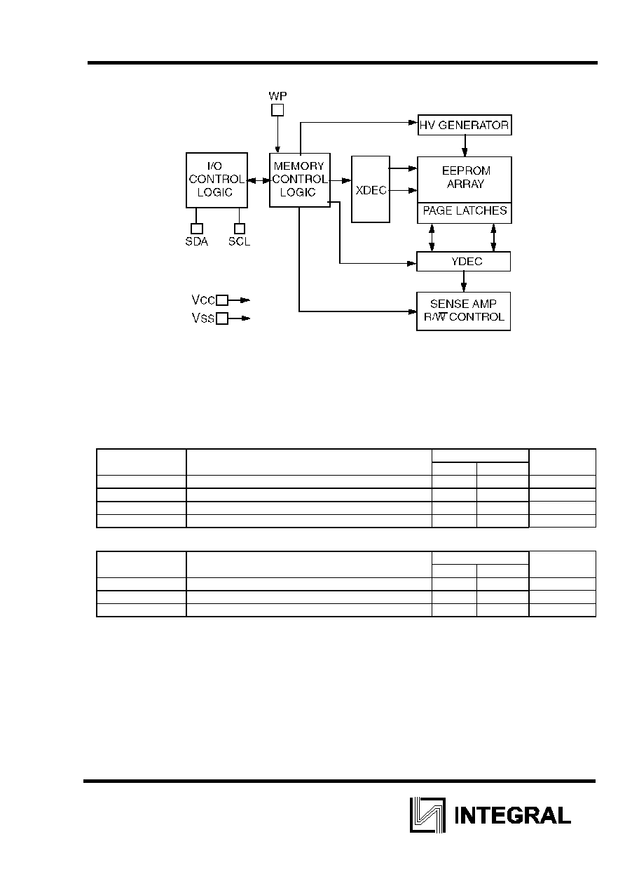
BLOCK DIAGRAM
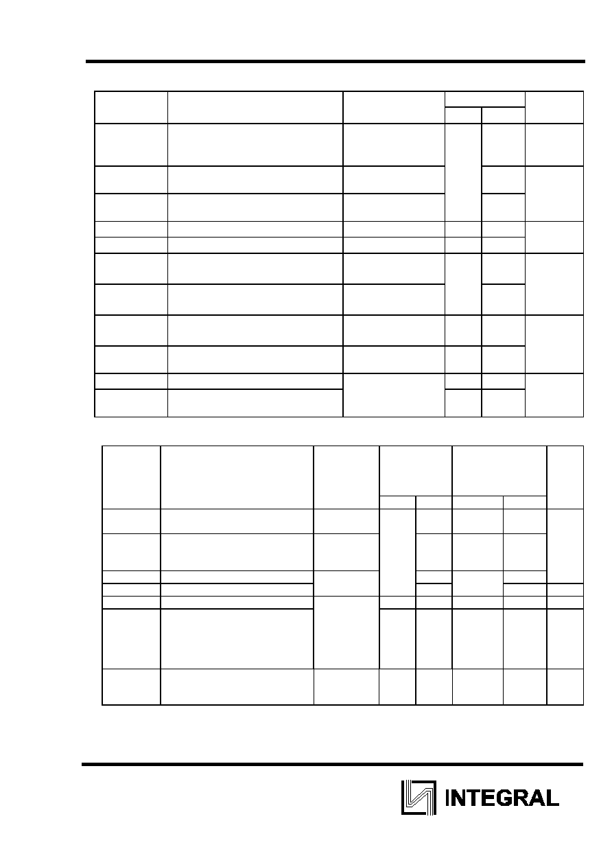
ELECTRICAL CHARACTERISTICS
Absolute Maximum Ratings*
Value
Symbol Parameter
min max
Unit
V
CC
Supply voltage
0
7.0
V
V
I
Input
voltage
-0.3
V
CC
+1V V
“
Storage temperature
-65
150
Ó
C
Ta Ambient
temperature
-65
125
Ó
C
Maximum Ratings
Value
Symbol Parameter
min max
Unit
V
CC
Supply
voltage
2.5
5.5 V
I
OL
Low level output current
-
3.0
mA
“
Operating ambient temperature
-40
85
Ó
C
IN24LC16
3
DC CHARACTERISTICS (Vcc = +2.5V to +5.5V Tamb = -40úC to +85úC)
Value
Symbol
Parameter
Mode of
measurements
Min Max
Unit
I
CCS
Standby current
Vcc = 3.0 V
Vcc = 5.5 V
SDA=SCL= Vcc
- 30
100
uA
I
——O(RD)
Operating current (read mode)
f
SCL
= 400 kHz
Vcc = 5.5 V
1.0 mA
I
——O(E/WR)
Operating current (erase/write mode)
f
SCL
= 400 kHz
Vcc = 5.5 V
3.0
I
LI
Input leakage current
V
IN
= (0.1 - 5.5) V
-10
10
uA
I
LŒ
Output leakage current
V
ŒUT
=
(0.1- 5.5) V
-10 10
—
IN
Input pin capacitance
V
——
=5.0 B, f=1 MHz
“ = 25
Ó
C
- 10 pF
—
out
Output pin capacitance
V
——
=5.0V,
f=1 MHz “ = 25
Ó
C
10
V
HYS
Hysteresis of Schmitt trigger
inputs
0.05
Vcc
- V
V
OL
Low level output voltage
I
OL
= 3.0 mA,
V
——
= 2.5 V
- 0.4
t
S
Time of data storage
“ = 25
Ó
C 200
- years
N
—(E/WR)
Number of ERASE/WRITE cycles
guaranteed
10000
00
pcs
AC CHARACTERISTICS
Standard
mode
(V
CC
=2.5
ü 5.5 V)
Speed
mode
(V
CC
=4.5
ü 5.5 V)
Unit
Symbol Parameter Mode
of
measure-
ments
min max min max
t
SP
Input filter spike suppression
(SDA and SCL pins)
-
50
-
50
ns
t
OF
Output fall time from VIH
minimum to VIL maximum
I
OL
= 3 mA,
—‚
<100 pF
250
20+0.1—‚
250
t
¿(SCL)
Output valid from clock
Note 2
3500
-
900
t
CY(E/WR)
Write cycle time (byte or page)
10
10
ms
f
SCL
Clock
frequency
- 100 -
400 kHz
t
BUF
Bus free time: Time the bus
must be
free before a new transmission
can
start
Note 2
4.7 - 1.3 - us
t
SU.STA
START condition setup time
For recurrent
signal
Note 2
4.7
0.6
IN24LC16
4
Standard
mode
(V
CC
=2.5
ü 5.5 V)
Speed
mode
(V
CC
=4.5
ü 5.5 V)
Unit
Symbol Parameter Mode
of
measure-
ments
min max min max
t
HD, STA
START condition hold time
Note 2
4.0
0.6
t
LOW
Clock high time
4.7
1.3
t
HIGH
Clock low time
4.0
0.6
t
r
SDA and SCL rise time
-
1000
-
300
ns
t
f
SDA and SCL fall time
300
300
t
HD. DAT
Data input hold time
Note 1, 2
0
-
0
-
t
SU. DAT
Data input setup time
Note 2
250
100
t
SU. STŒ
STOP condition setup time
4
0.6
us
Notes
1. As a transmitter, the device must provide an internal minimum delay time to bridge the undefined region (minimum
300 ns) of the falling edge of SCL to avoid unintended generation of START or STOP conditions.
2. This parameter is not tested but guaranteed by characterization.
—
¬
-
total bus capacity
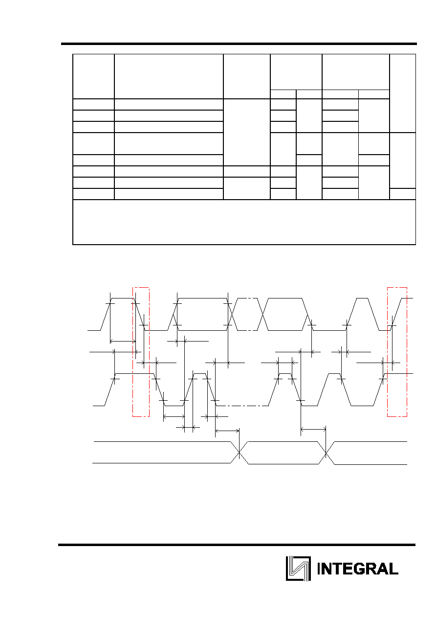
BUS TIMING DATA
Data
Data
Data
t
r
t
f
1
8
9
0.9
0.1
0.1
0.9
SDA
IN
SCL
S
T
SP
SDA
out
t
A(SCL)
t
A(SCL)
t
SU.STA
t
HD.STA
t
HD.DAT
t
SU.STO
t
HD.ACK
t
SU.ACK
t
HIGH
t
LOW
t
BUF
t
SU.DAT
IN24LC16
5
FUNCTIONAL DESCRIPTION
The 24LC16B supports a Bi-directional 2-wire bus and data transmission protocol. A device that sends data
onto the bus is defined as transmitter, and a device receiving data as receiver. The bus has to be controlled
by a master device which generates the serial clock (SCL), controls the bus access, and generates the
START and STOP conditions, while the 24LC16B works as slave. Both, master and slave can operate as
transmitter or receiver but the master device determines which mode is activated.
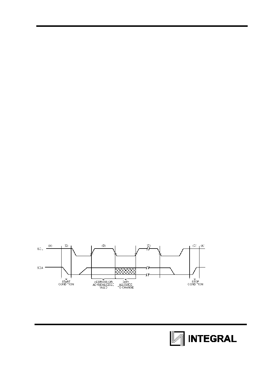
BUS CHARACTERISTICS
The following bus protocol has been defined:
û Data transfer may be initiated only when the bus is not busy.
û During data transfer, the data line must remain stable whenever the clock line is HIGH. Changes in the
data line while the clock line is HIGH will be interpreted as a START or STOP condition.
Accordingly, the following bus conditions have been defined
Bus not Busy (A)
Both data and clock lines remain HIGH.
Start Data Transfer (B)
A HIGH to LOW transition of the SDA line while the clock (SCL) is HIGH determines a START condition. All
commands must be preceded by a START condition.
Stop Data Transfer (C)
A LOW to HIGH transition of the SDA line while the clock (SCL) is HIGH determines a STOP condition. All
operations must be ended with a STOP condition.
Data Valid (D)
The state of the data line represents valid data when, after a START condition, the data line is stable for the
duration of the HIGH period of the clock signal.
The data on the line must be changed during the LOW period of the clock signal. There is one clock pulse
per bit of data.
Each data transfer is initiated with a START condition and terminated with a STOP condition. The number of
the data bytes transferred between the START and STOP conditions is determined by the master device
and is theoretically unlimited, although only the last sixteen will be stored when doing a write operation.
When an overwrite does occur it will replace data in a first in first out fashion.
Acknowledge
Each receiving device, when addressed, is obliged to generate an acknowledge after the reception of each
byte. The master device must generate an extra clock pulse which is associated with this acknowledge bit.
Note: The 24LC16B does not generate any acknowledge bits if an internal programming cycle is in
progress.
The device that acknowledges, has to pull down the SDA line during the acknowledge clock pulse in such a
way that the SDA line is stable LOW during the HIGH period of the acknowledge related clock pulse. Of
course, setup and hold times must be taken into account. During reads, a master must signal an end of data
to the slave by not generating an acknowledge bit on the last byte that has been clocked out of the slave. In
this case, the slave (24LC16B) will leave the data line HIGH to enable the master to generate the STOP
condition.
DATA TRANSFER SEQUENCE ON THE SERIAL BUS
Device Addressing
A control byte is the first byte received following the start condition from the master device. The control byte
consists of a four bit control code, for the 24LC16B this is set as 1010 binary for read and write operations.
The next three bits of the control byte are the block select bits (B2, B1, B0). They are used by the master
device to select which of the eight 256 word blocks of memory are to be accessed. These bits are in effect