 | –≠–ª–µ–∫—Ç—Ä–æ–Ω–Ω—ã–π –∫–æ–º–ø–æ–Ω–µ–Ω—Ç: IN74123 | –°–∫–∞—á–∞—Ç—å:  PDF PDF  ZIP ZIP |

TECHNICAL DATA
IN74123
Dual Monostable Multivibrator
with Clear
ORDERING INFORMATION
IN74123N Plastic
T
A
= -10
ú to 70ú C for package
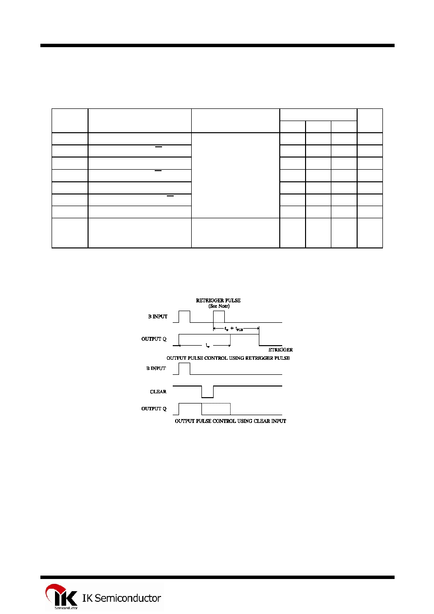
The IN74123 multivibrator feature d-c triggering from gated low-
level-active (A) and high-level-active (B) inputs, and also provide
overriding direct clear inputs. Complementary outputs are provided. The
retrigger capability simplifies the output pulse is terminated, the output
pulse may be extended. The overriding clear capability permits any output
pulse to be terminated at a predetermined time independently of the
timing components R and C. Figure 1 illustrates triggering the one-shot
with the high-level-active (B) inputs.
LOGIC DIAGRAM
Pin 16 = V
CC
Pin 8 = GND
Timing Component
Connections when
C
EXT
ò 1000 pF
Timing Component Connections when
C
EXT >
1000 pF and Clear is used
PIN ASSIGNMENT
FUNCTION TABLE
Inputs Outputs
Clear
A B Q Q
L X X L H
X H X L H
X X L L H
H L
H H
L
H
X = don't care
1

IN74123
MAXIMUM RATINGS
*
Symbol Parameter
Value
Unit
V
CC
Supply Voltage
6.0
V
V
IN
Input Voltage
-0.5 to 6.0
V
Tstg
Storage Temperature Range
-65 to +150
úC
*
Maximum Ratings are those values beyond which damage to the device may accur.
RECOMMENDED OPERATING CONDITIONS
Symbol Parameter Min
Max
Unit
V
CC
Supply Voltage
4.75
5.25
V
V
IH
High Level Input Voltage
2.0
V
V
IL
Low Level Input Voltage
0.8
V
I
OL
Low Level Output Current
16
mA
I
OH
High Level Output Current
-0.8
mA
R
EXT
External Timing Resistance
5.0
50
k
C
EXT
External Capacitance
No Restriction
R
EXT
/C
EXT
Wiring Capacitance at R
EXT
/C
EXT
Terminale
50
pF
T
A
Operating Temperature
-10
+70
úC
t
W
Pulse Width
A or B inputs high
40
50
ns
A or B inputs low
40
50
Clear
low
40
50
DC ELECTRICAL CHARACTERISTICS
(T
A
=+25
úC)
Symbol
Parameter
Test Conditions
Guaranteed Limit
Unit
Min
Typ
Max
V
IK
Input Clamp Voltage
V
CC
=min, I
IN
=-12 mA
-1.5
V
V
OH
High-Level Output
Voltage
V
CC
=min, I
OH
=-0.8 mA
V
IL
=0.8 V, V
IH
=2.0 V
2.4 3.5 V
V
OL
Low-Level Output
Voltage
V
CC
=min, I
OL
=16 mA
V
IL
=0.8 V, V
IH
=2.0 V
0.3
0.4
V
I
IH
High Level Input
V
CC
=max,
A, B inputs
40
A
Current
V
IN
=2.4V
Clear
input 80
I
I
Input Current at
Maximum Input Voltage
V
CC
=max, V
IN
=5.5 V
1.0
mA
I
IL
Low Level Input
V
CC
=max,
A, B inputs
-1.6
mA
Current
V
IN
=0.4V Clear
input
-3.2
I
OS
Short Circuit Current
One Output Shorted at a
Time
V
CC
=max, V
O
=0 V
-10
-40
mA
I
CC
Supply Current
V
CC
=max
47
66
mA
2
IN74123
AC ELECTRICAL CHARACTERISTICS
(V
CC
=5.0 V, T
A
=+25
úC, Input t
r
=t
f
=6.0 ns)
Symbol
Parameter
Test Conditions
Guaranteed Limit
Unit
Min
Typ
Max
t
PLH
Propagation Delay, A to Q
32
33
ns
t
PHL
Propagation Delay, A to Q
30
40
ns
t
PLH
Propagation Delay, B to Q
C
EXT
=0, R
EXT
=5.1 k
,
19 28 ns
t
PHL
Propagation Delay, B to Q
C
L
=15 pF,R
L
=390
27 36 ns
t
PLH
Propagation Delay, Clear to Q
30
40
ns
t
PHL
Propagation Delay, Clear to Q
18
27
ns
t
WQmin
Pulse Width, A or B to Q
45
65
ns
t
WQ
Pulse Width, A or B to Q
C
EXT
=1000 pF,
R
EXT
=10 k
,
R
L
=390
,C
L
=15 pF
2.76
3.2 3.37
s
NOTE: Retrigger pulse must not start before 0.22 C
EXT
(in picofarads) nonoseconds after previous trigger pulse.
Figure 1. Typical Input/Output Pulses
3
IN74123
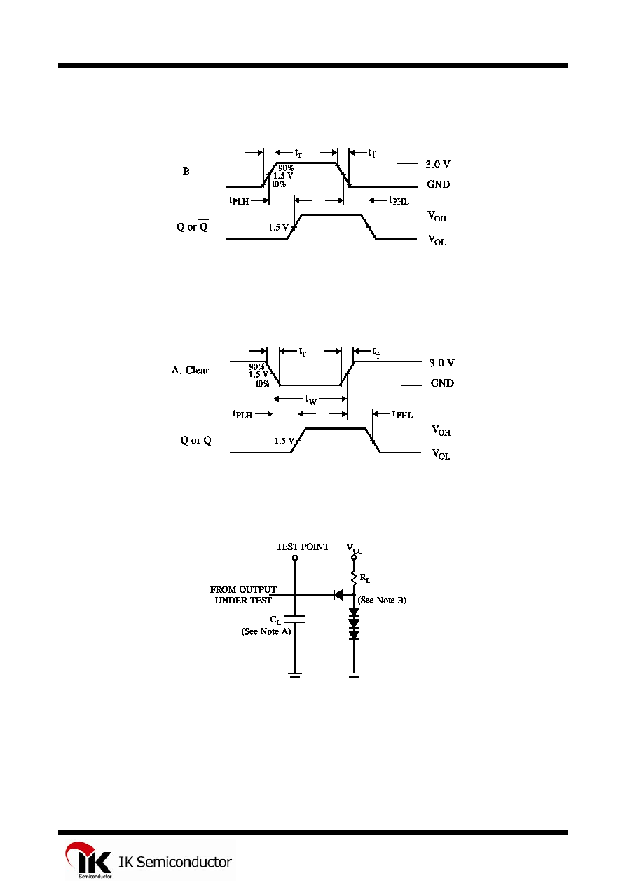
Figure 2. Switching Waveforms
Figure 3. Switching Waveforms
NOTES A. C
L
includes probe and jig capacitance.
B. All diodes are 1N916 or 1N3064/
Figure 4. Test Circuit
4
IN74123
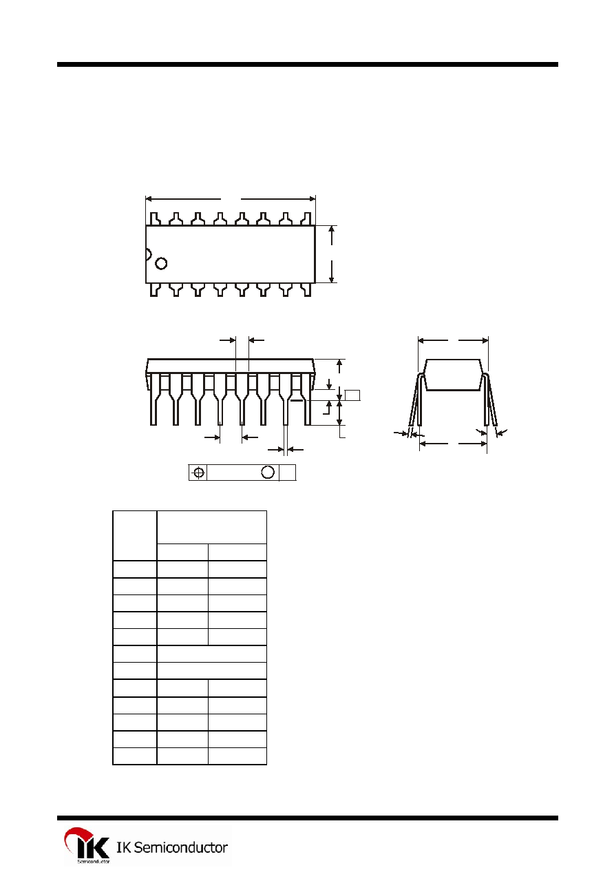
N SUFFIX PLASTIC
(MS - 001BB)
L
H
M
J
A
B
F
G
D
SEATING
PLANE
N
K
0.25 (0.010) M T
-T-
C
1
16
8
9
Dimensions, mm
Symbol MIN MAX
A 18.67 19.69
B 6.10 7.11
C 5.33
D 0.36 0.56
F 1.14 1.78
G 2.54
H 7.62
J
0
ú 10ú
K 2.92 3.81
L 7.62 8.26
M 0.20 0.36
N 0.38
1.
.
NOTES:
Dimensions "A", "B" do not include mold flash or
protrusions. Maximum mold flash or protrusions 0.25 mm
(0.010) per side
5