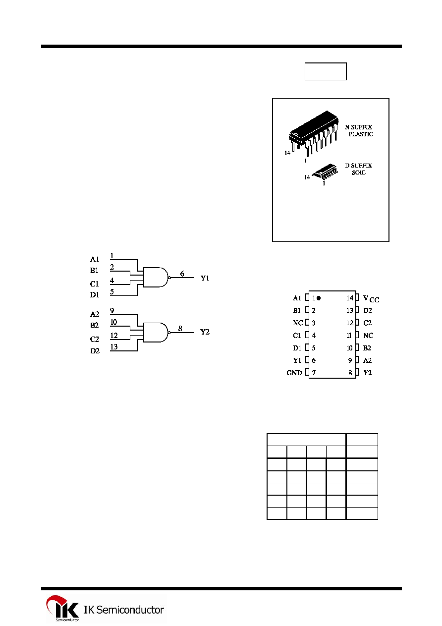
TECHNICAL DATA
IN7440
Dual 4-Input Positive-NAND Buffers
ORDERING INFORMATION
IN7440N Plastic
IN7440D SOIC
T
A
= -10
ú to 70ú C for all packages
LOGIC DIAGRAM
PIN 14 =V
CC
PIN 7 = GND
PIN ASSIGNMENT
NC - No internal connection
FUNCTION TABLE
Inputs Output
A B C D Y
L X
X X H
X
L X X H
X
X
L X H
X
X
X L H
H
H
H H L
X =don't care
1
IN7440
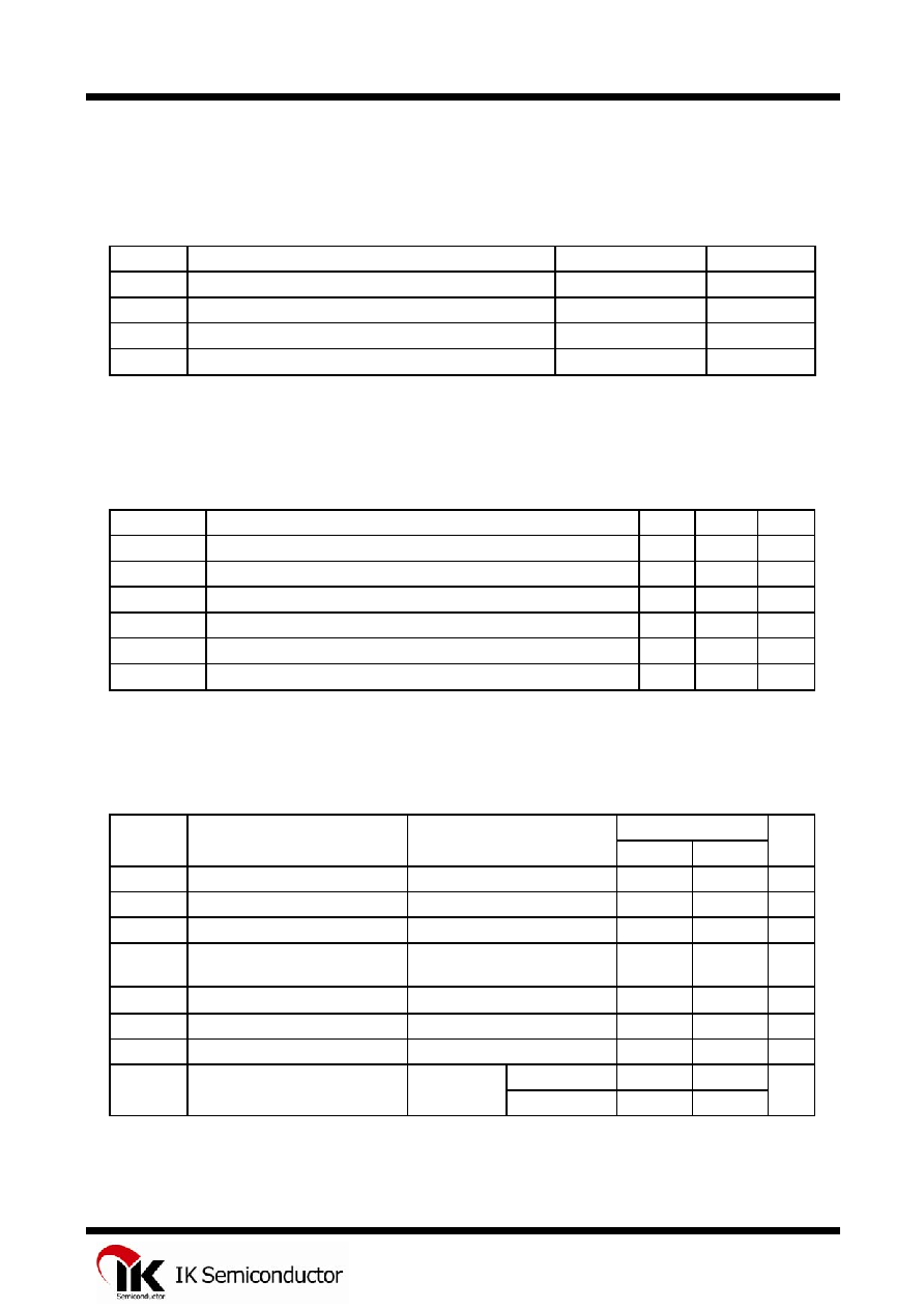
MAXIMUM RATINGS
*
Symbol Parameter
Value
Unit
V
CC
Supply Voltage
7.0
V
V
IN
Input Voltage
5.5
V
I
OL
Low Level Output Current
48
mA
Tstg
Storage Temperature Range
-65 to +150
úC
*
Maximum Ratings are those values beyond which damage to the device may occur.
Functional operation should be restricted to the Recommended Operating Conditions.
RECOMMENDED OPERATING CONDITIONS
Symbol Parameter
Min
Max
Unit
V
CC
Supply Voltage
4.75
5.25
V
V
IH
High Level Input Voltage
2.0
V
V
IL
Low Level Input Voltage
0.8
V
I
OH
High Level Output Current
-1.2
mA
I
OL
Low Level Output Current
48
mA
T
A
Ambient Temperature Range
-10
+70
úC
DC ELECTRICAL CHARACTERISTICS over full operating conditions
Guaranteed
Limit
Symbol Parameter
Test
Conditions
Min
Max
Unit
V
IK
Input Clamp Voltage
V
CC
= min, I
IN
= -10 mA
-1.5
V
V
OH
High Level Output Voltage
V
CC
= min, I
OH
=max
2.4
V
V
OL
Low Level Output Voltage
V
CC
= min, I
OL
=max
0.4
V
I
I
Input Current at Maximum
Input Voltage
V
CC
= max, V
IN
= 5.5 V
1
mA
I
IH
High Level Input Current
V
CC
= max, V
IN
= 2.4 V
40
A
I
IL
Low Level Input Current
V
CC
= max, V
IN
= 0.4 V
-1.6
mA
I
OS
*
Short-Circuit Output Current
-18
-70
mA
I
CC
Supply Current
V
CC
= max
Outputs High
8
mA
Outputs
Low
27
*Not more than one output should be shorted at a time, and duration of the short-circuit should not exceed one second
.
2
IN7440
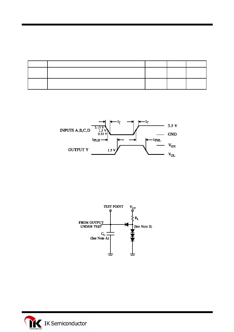
AC ELECTRICAL CHARACTERISTICS
(T = 25
úC, V
CC
= 5.0 V, C
L
= 15 pF,
R
L
= 130
, Input t
r
= t
f
= 10 ns)
Symbol Parameter Min
Max
Unit
t
PLH
Propagation Delay Time, Low to High Level Output (from
Input to Output)
22
ns
t
PHL
Propagation Delay Time, High to Low Level Output (from
Input to Output)
15
ns
Figure 1. Switching Waveforms
NOTES A. C
L
includes probe and jig capacitance.
B. All diodes are 1N916 or 1N3064.
Figure 2. Test Circuit
3
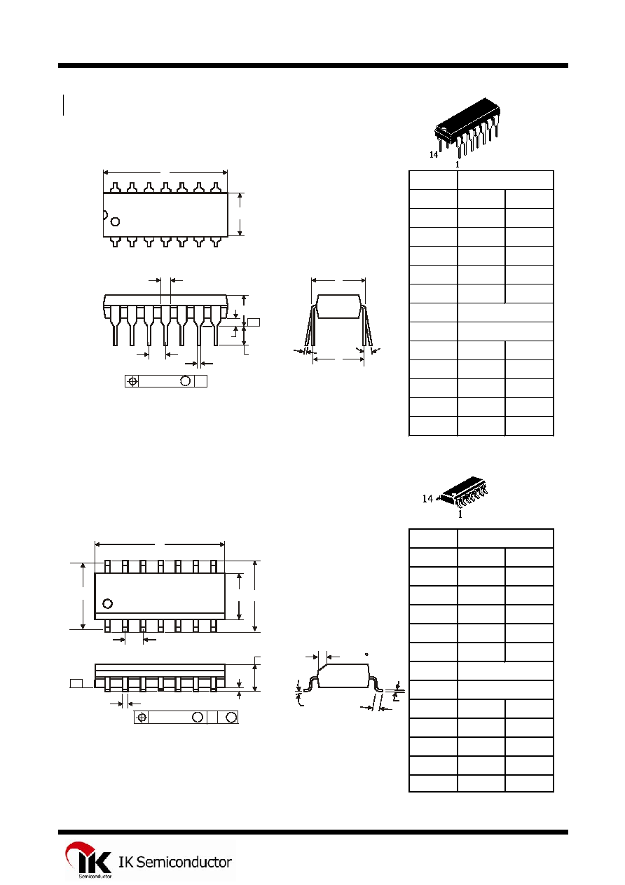
IN7440
N SUFFIX PLASTIC DIP
(MS - 001AA)
Symbol
MIN
MAX
A
18.67
19.69
B
6.1
7.11
C
5.33
D
0.36
0.56
F
1.14
1.78
G
H
J
0
ú
10
ú
K
2.92
3.81
NOTES:
L
7.62
8.26
1.
Dimensions "A", "B" do not include mold flash or protrusions.
M
0.2
0.36
Maximum mold flash or protrusions 0.25 mm (0.010) per side.
N
0.38
D SUFFIX SOIC
(MS - 012AB)
Symbol
MIN
MAX
A
8.55
8.75
B
3.8
4
C
1.35
1.75
D
0.33
0.51
F
0.4
1.27
G
H
J
0ú
8ú
NOTES:
K
0.1
0.25
1.
Dimensions A and B do not include mold flash or protrusion.
M
0.19
0.25
2.
Maximum mold flash or protrusion 0.15 mm (0.006) per side
P
5.8
6.2
for A; for B 0.25 mm (0.010) per side.
R
0.25
0.5
Dimension, mm
1.27
5.27
2.54
7.62
Dimension, mm
A
B
H
C
K
C M
J
F
M
P
G
D
R x 45
SEATING
PLANE
0.25 (0.010) M T
-T-
1
14
7
8
A
B
F
G
D
L
H
SEATING
PLANE
N
K
0.25 (0.010) M T
M
J
-T-
C
1
14
7
8
4