 | –≠–ª–µ–∫—Ç—Ä–æ–Ω–Ω—ã–π –∫–æ–º–ø–æ–Ω–µ–Ω—Ç: IN74AC534 | –°–∫–∞—á–∞—Ç—å:  PDF PDF  ZIP ZIP |
TECHNICAL DATA
446
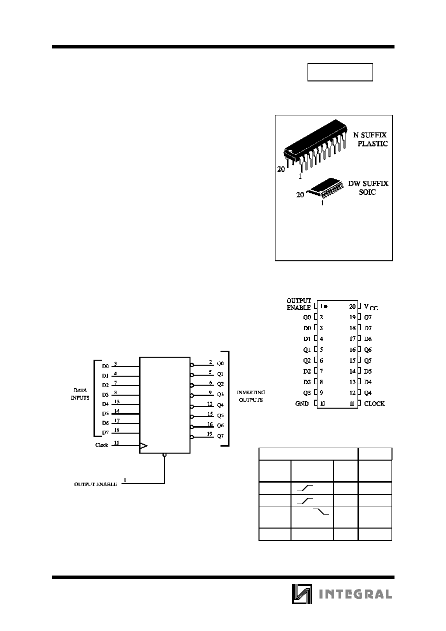
Octal 3-State
Inverting D Flip-Flop
High-Speed Silicon-Gate CMOS
The IN74AC534 is identical in pinout to the LS/ALS534,
HC/HCT534. The device inputs are compatible with standard CMOS
outputs; with pullup resistors, they are compatible with LS/ALS
outputs.
Data meeting the setup time is clocked, in inverted form, to the
outputs with the rising edge of the Clock. The Output Enable input
does not affect the states of the flip-flops, but when Output Enable is
high, the outputs are forced to the high impedance state. Thus, data
may be stored even when the outputs are not enabled.
û
Outputs Directly Interface to CMOS, NMOS, and TTL
û
Operating Voltage Range: 2.0 to 6.0 V
û
Low Input Current: 1.0
A; 0.1
A @ 25
ú
C
û
High Noise Immunity Characteristic of CMOS Devices
û
Outputs Source/Sink 24 mA
IN74AC534
ORDERING INFORMATION
IN74AC534N Plastic
IN74AC534DW SOIC
T
A
= -40
ú
to 85
ú
C for all
packages
LOGIC DIAGRAM
PIN 20=V
CC
PIN 10 = GND
FUNCTION TABLE
Inputs
Output
Output
Enable
Clock
D
Q
L
H
L
L
L
H
L
L,H,
X
no
change
H
X
X
Z
X = don't care
Z = high impedance
PIN ASSIGNMENT
IN74AC534
447
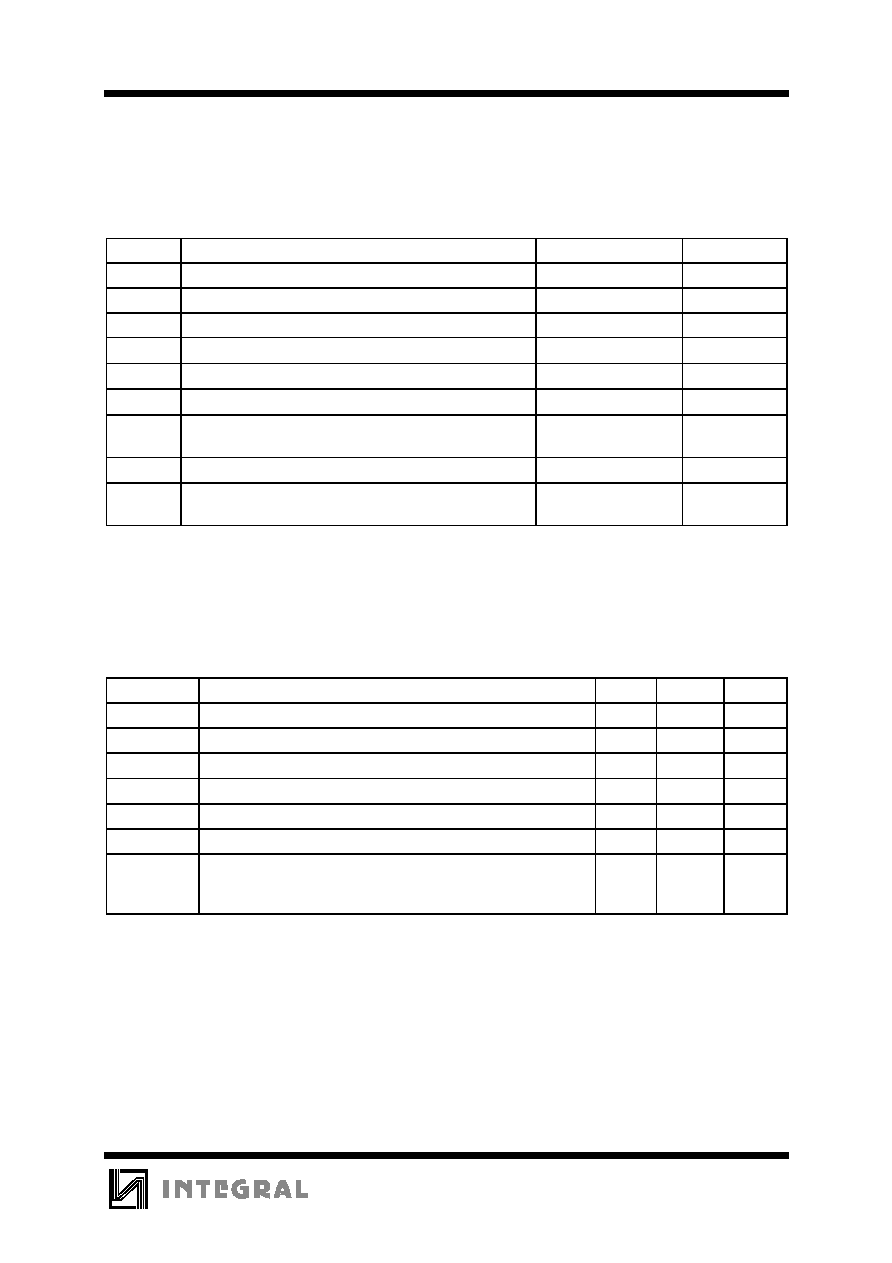
MAXIMUM RATINGS
*
Symbol
Parameter
Value
Unit
V
CC
DC Supply Voltage (Referenced to GND)
-0.5 to +7.0
V
V
IN
DC Input Voltage (Referenced to GND)
-0.5 to V
CC
+0.5
V
V
OUT
DC Output Voltage (Referenced to GND)
-0.5 to V
CC
+0.5
V
I
IN
DC Input Current, per Pin
20
mA
I
OUT
DC Output Sink/Source Current, per Pin
50
mA
I
CC
DC Supply Current, V
CC
and GND Pins
50
mA
P
D
Power Dissipation in Still Air, Plastic DIP+
SOIC Package+
750
500
mW
Tstg
Storage Temperature
-65 to +150
ú
C
T
L
Lead Temperature, 1 mm from Case for 10 Seconds
(Plastic DIP or SOIC Package)
260
ú
C
*
Maximum Ratings are those values beyond which damage to the device may occur.
Functional operation should be restricted to the Recommended Operating Conditions.
+Derating - Plastic DIP: - 10 mW/
ú
C from 65
ú
to 125
ú
C
SOIC Package: : - 7 mW/
ú
C from 65
ú
to 125
ú
C
RECOMMENDED OPERATING CONDITIONS
Symbol
Parameter
Min
Max
Unit
V
CC
DC Supply Voltage (Referenced to GND)
2.0
6.0
V
V
IN
, V
OUT
DC Input Voltage, Output Voltage (Referenced to GND)
0
V
CC
V
T
J
Junction Temperature (PDIP)
140
ú
C
T
A
Operating Temperature, All Package Types
-40
+85
ú
C
I
OH
Output Current - High
-24
mA
I
OL
Output Current - Low
24
mA
t
r
, t
f
Input Rise and Fall Time
*
(except Schmitt Inputs)
V
CC
=3.0 V
V
CC
=4.5 V
V
CC
=5.5 V
0
0
0
150
40
25
ns/V
*
V
IN
from 30% to 70% V
CC
This device contains protection circuitry to guard against damage due to high static voltages or electric
fields. However, precautions must be taken to avoid applications of any voltage higher than maximum rated
voltages to this high-impedance circuit. For proper operation, V
IN
and V
OUT
should be constrained to the range
GND
ò
(V
IN
or V
OUT
)
ò
V
CC
.
Unused inputs must always be tied to an appropriate logic voltage level (e.g., either GND or V
CC
).
Unused outputs must be left open.
IN74AC534
448
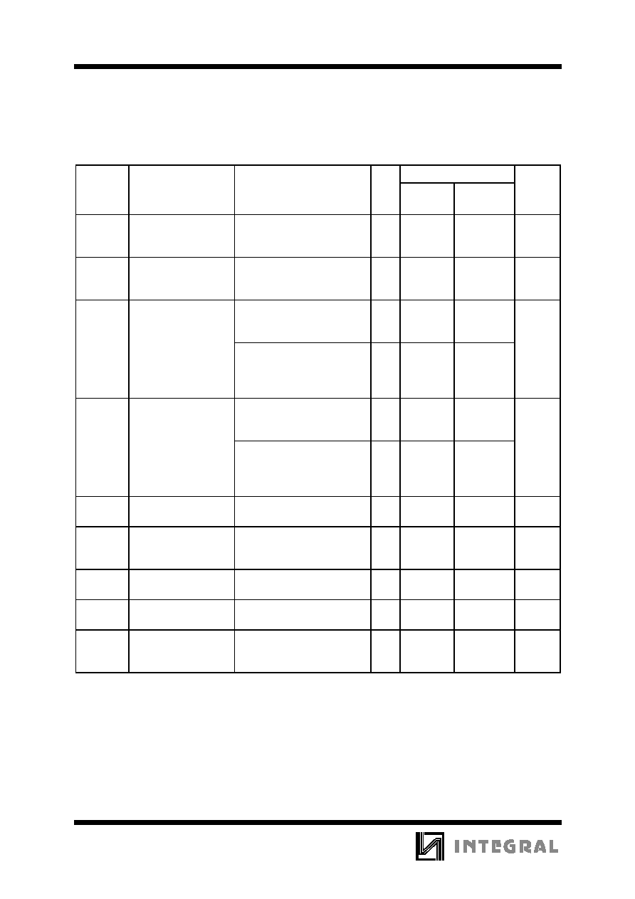
DC ELECTRICAL CHARACTERISTICS
(Voltages Referenced to GND)
V
CC
Guaranteed Limits
Symbol
Parameter
Test Conditions
V
25
ú
C
-40
ú
C to
85
ú
C
Unit
V
IH
Minimum High-Level
Input Voltage
V
OUT
=0.1 V or V
CC
-0.1 V
3.0
4.5
5.5
2.1
3.15
3.85
2.1
3.15
3.85
V
V
IL
Maximum Low -
Level Input Voltage
V
OUT
=0.1 V or V
CC
-0.1 V
3.0
4.5
5.5
0.9
1.35
1.65
0.9
1.35
1.65
V
V
OH
Minimum High-Level
Output Voltage
I
OUT
ò
-50
A
3.0
4.5
5.5
2.9
4.4
5.4
2.9
4.4
5.4
V
*
V
IN
=V
IH
or V
IL
I
OH
=-12 mA
I
OH
=-24 mA
I
OH
=-24 mA
3.0
4.5
5.5
2.56
3.86
4.86
2.46
3.76
4.76
V
OL
Maximum Low-Level
Output Voltage
I
OUT
ò
50
A
3.0
4.5
5.5
0.1
0.1
0.1
0.1
0.1
0.1
V
*
V
IN
=V
IH
or V
IL
I
OL
=12 mA
I
OL
=24 mA
I
OL
=24 mA
3.0
4.5
5.5
0.36
0.36
0.36
0.44
0.44
0.44
I
IN
Maximum Input
Leakage Current
V
IN
=V
CC
or GND
5.5
0.1
1.0
A
I
OZ
Maximum Three-
State Leakage
Current
V
IN
(OE)= V
IH
or V
IL
V
IN
=V
CC
or GND
V
OUT
=V
CC
or GND
5.5
0.5
5.0
A
I
OLD
+Minimum Dynamic
Output Current
V
OLD
=1.65 V Max
5.5
75
mA
I
OHD
+Minimum Dynamic
Output Current
V
OHD
=3.85 V Min
5.5
-75
mA
I
CC
Maximum Quiescent
Supply Current
(per Package)
V
IN
=V
CC
or GND
5.5
8.0
80
A
*
All outputs loaded; thresholds on input associated with output under test.
+Maximum test duration 2.0 ms, one output loaded at a time.
Note: I
IN
and I
CC
@ 3.0 V are guaranteed to be less than or equal to the respective limit @ 5.5 V V
CC
IN74AC534
449
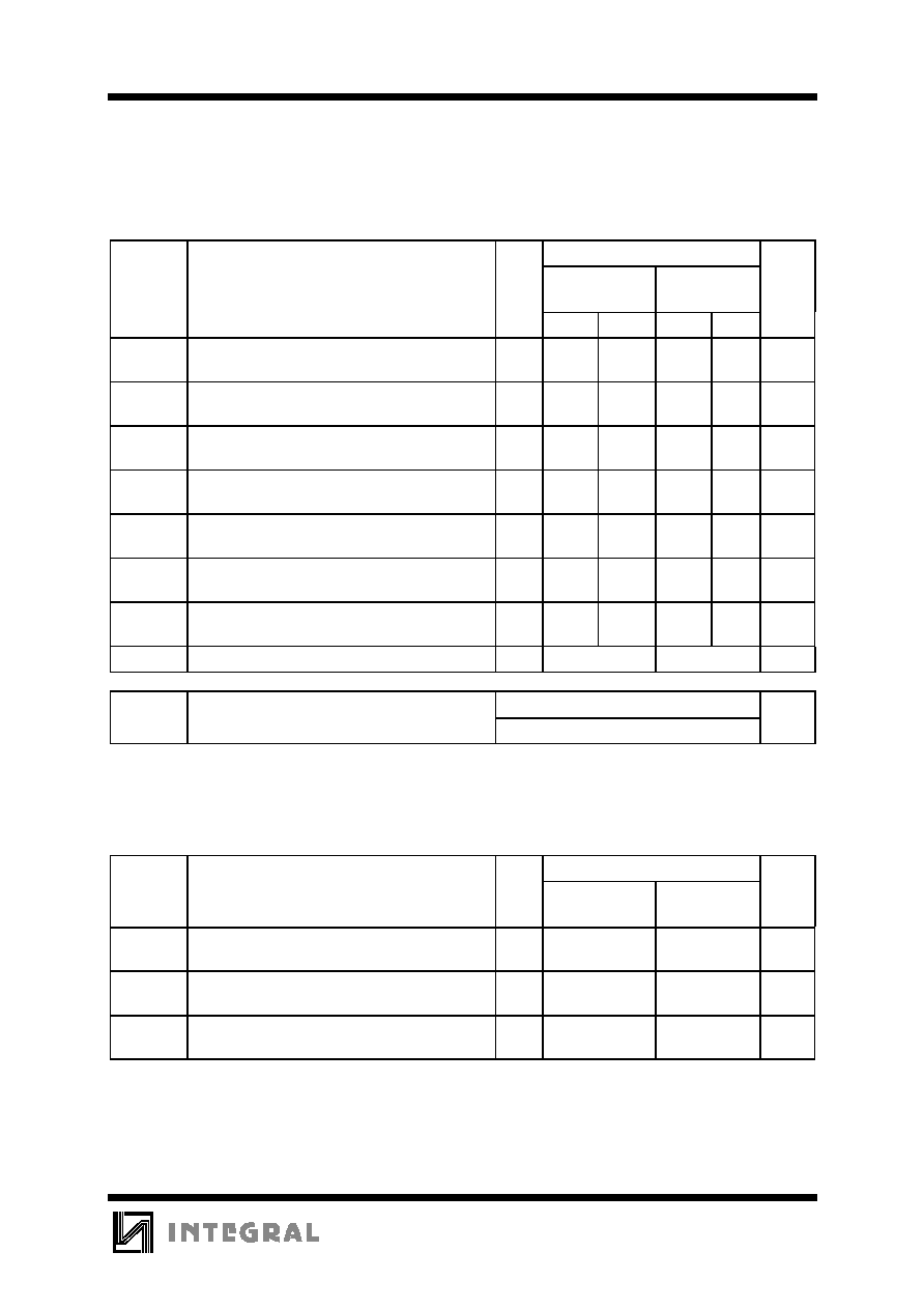
AC ELECTRICAL CHARACTERISTICS
(C
L
=50pF,Input t
r
=t
f
=3.0 ns)
V
CC
*
Guaranteed Limits
Symbol
Parameter
V
25
ú
C
-40
ú
C to
85
ú
C
Unit
Min
Max
Min
Max
f
max
Maximum Clock Frequency (Figure 1)
3.3
5.0
70
150
70
140
MHz
t
PLH
Propagation Delay, Clock to Q (Figure 1)
3.3
5.0
3.0
2.5
14.0
10.5
2.5
2.0
16.0
12.0
ns
t
PHL
Propagation Delay, Clock to Q (Figure 1)
3.3
5.0
3.0
2.5
13.0
9.5
2.5
2.0
15.0
11.0
ns
t
PZH
Propagation Delay, Output Enable to Q
(Figure 2)
3.3
5.0
3.0
2.5
12.5
10.0
2.5
2.0
14.0
11.5
ns
t
PZL
Propagation Delay, Output Enable to Q
(Figure 2)
3.3
5.0
3.0
2.5
12.5
10.0
2.5
2.0
14.0
11.5
ns
t
PHZ
Propagation Delay, Output Enable to Q
(Figure 2)
3.3
5.0
2.0
1.5
13.5
11.5
1.5
1.0
15.0
12,5
ns
t
PLZ
Propagation Delay, Output Enable to Q
(Figure 2)
3.3
5.0
2.0
1.5
12.0
10.0
1.5
1.0
13.5
11.0
ns
C
IN
Maximum Input Capacitance
5.0
4.5
4.5
pF
Typical @25
ú
C,V
CC
=5.0 V
C
PD
Power Dissipation Capacitance
40
pF
*
Voltage Range 3.3 V is 3.3 V
0.3 V
Voltage Range 5.0 V is 5.0 V
0.5 V
TIMING REQUIREMENTS
(C
L
=50pF,Input t
r
=t
f
=3.0 ns)
V
CC
*
Guaranteed Limits
Symbol
Parameter
V
25
ú
C
-40
ú
C to
85
ú
C
Unit
t
su
Minimum Setup Time, Data to Clock
(Figure 3)
3.3
5.0
5.0
3.5
6.5
4.0
ns
t
h
Minimum Hold Time, Clock to Data
(Figure 3)
3.3
5.0
1.0
1.0
1.5
1.5
ns
t
w
Minimum Pulse Width, Clock (Figure 1)
3.3
5.0
5.0
3.5
6.5
4.0
ns
*
Voltage Range 3.3 V is 3.3 V
0.3 V
Voltage Range 5.0 V is 5.0 V
0.5 V
IN74AC534
450
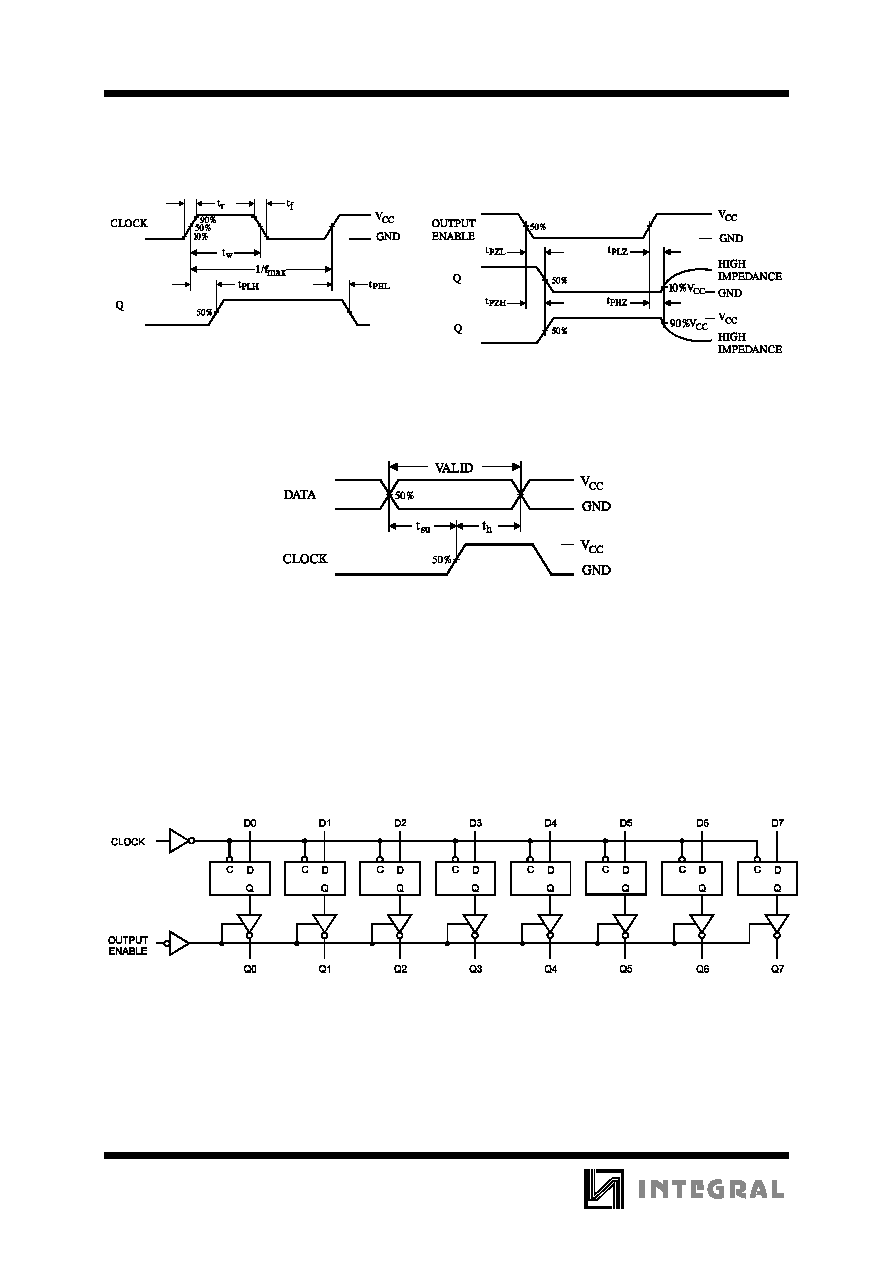
Figure 1. Switching Waveforms
Figure 2. Switching Waveforms
Figure 3. Switching Waveforms
EXPANDED LOGIC DIAGRAM