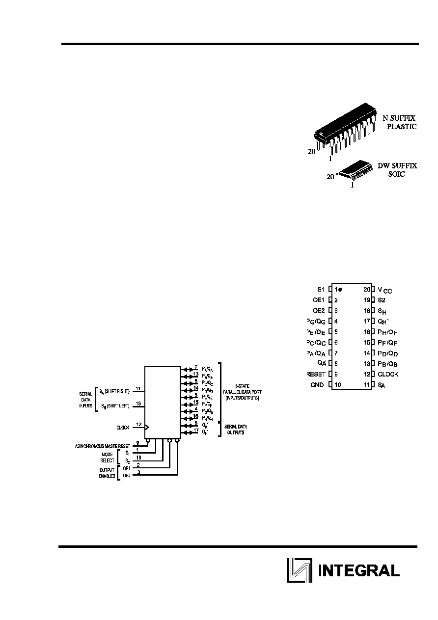
IN74ACT299
1
8-B
IT
B
IDIRECTIONAL
U
NIVERSAL
S
HIFT
R
EGISTER WITH
P
ARALLEL
I/O
High-Speed Silicon-Gate CMOS
The IN74ACT299 is identical in pinout to the LS/ALS299,
HC/HCT299. The IN74ACT299 may be used as a level converter
for interfacing TTL or NMOS outputs to High Speed CMOS inputs.
The IN74ACT299 features a multiplexed parallel input/output
data port to achieve full 8-bit handling in a 20 pin package. Due to
the large output drive capability and the 3-state feature, this
device is ideally suited for interface with bus lines in a bus-
oriented system.
Two Mode-Select inputs and two Output Enable inputs are
used to choose the mode of operation as listed in the Function
Table. Synchronous parallel loading is accomplished by taking
both Mode-Select lines, S
1
and S
2
, high. This places the outputs in
the high-impedance state, which permits data applied to the data
port to be clocked into the register. Reading out of the register can
be accomplished when the outputs are enabled. The active-low
asynchronous Reset overrides all other inputs.
� TTL/NMOS Compatible Input Levels
� Outputs Directly Interface to CMOS, NMOS, and TTL
� Operating Voltage Range: 4.5 to 5.5 V
� Low Input Current: 1.0 A; 0.1 A @ 25�C
� Outputs Source/Sink 24 mA
ORDERING INFORMATION
IN74ACT299N Plastic
IN74ACT299DW SOIC
T
A
= -40
� to 85� C for all
packages
PIN ASSIGNMENT
LOGIC DIAGRAM
PIN 20=V
CC
PIN 10 = GND
IN74ACT299
2
MAXIMUM RATINGS
*
Symbol Parameter
Value
Unit
V
CC
DC Supply Voltage (Referenced to GND)
-0.5 to +7.0
V
V
IN
DC Input Voltage (Referenced to GND)
-0.5 to V
CC
+0.5
V
V
OUT
DC Output Voltage (Referenced to GND)
-0.5 to V
CC
+0.5
V
I
IN
DC Input Current, per Pin
20
mA
I
OUT
DC Output Sink/Source Current, per Pin
50
mA
I
CC
DC Supply Current, V
CC
and GND Pins
50
mA
P
D
Power Dissipation in Still Air, Plastic DIP+
SOIC Package+
750
500
mW
Tstg
Storage Temperature
-65 to +150
�C
T
L
Lead Temperature, 1 mm from Case for 10
Seconds
(Plastic DIP or SOIC Package)
260
�C
*
Maximum Ratings are those values beyond which damage to the device may occur.
Functional operation should be restricted to the Recommended Operating Conditions.
+Derating - Plastic DIP: - 10 mW/
�C from 65� to 125�C
SOIC Package: : - 7 mW/
�C from 65� to 125�C
RECOMMENDED OPERATING CONDITIONS
Symbol Parameter Min
Max
Unit
V
CC
DC Supply Voltage (Referenced to GND)
4.5
5.5
V
V
IN
, V
OUT
DC Input Voltage, Output Voltage (Referenced to
GND)
0 V
CC
V
T
J
Junction Temperature (PDIP)
140
�C
T
A
Operating Temperature, All Package Types
-40
+85
�C
I
OH
Output Current - High
-24
mA
I
OL
Output Current - Low
24
mA
t
r
, t
f
Input Rise and Fall Time
*
(except Schmitt Inputs)
V
CC
=4.5 V
V
CC
=5.5 V
0
0
10
8.0
ns/V
*
V
IN
from 0.8 V to 2.0 V
This device contains protection circuitry to guard against damage due to high static
voltages or electric fields. However, precautions must be taken to avoid applications of any voltage
higher than maximum rated voltages to this high-impedance circuit. For proper operation, V
IN
and
V
OUT
should be constrained to the range GND
�(V
IN
or V
OUT
)
�V
CC
.
Unused inputs must always be tied to an appropriate logic voltage level (e.g., either GND or
V
CC
). Unused outputs must be left open.
IN74ACT299
3
DC ELECTRICAL CHARACTERISTICS(Voltages Referenced to GND)
V
CC
Guaranteed
Limits
Symbol Parameter
Test
Conditions V
25
�C -40�C to
85
�C
Unit
V
IH
Minimum High-
Level Input
Voltage
V
OUT
= 0.1 V or V
CC
-0.1
V
4.5
5.5
2.0
2.0
2.0
2.0
V
V
IL
Maximum Low -
Level Input
Voltage
V
OUT
= 0.1 V or V
CC
-0.1
V
4.5
5.5
0.8
0.8
0.8
0.8
V
V
OH
Minimum High-
Level Output
Voltage
I
OUT
� -50 A
4.5
5.5
4.4
5.4
4.4
5.4
V
*
V
IN
=V
IH
or V
IL
I
OH
=-24 mA
I
OH
=-24 mA
4.5
5.5
3.86
4.86
3.76
4.76
V
OL
Maximum Low-
Level Output
Voltage
I
OUT
� 50 A
4.5
5.5
0.1
0.1
0.1
0.1
V
*
V
IN
= V
IH
or V
IL
I
OL
=24 mA
I
OL
=24 mA
4.5
5.5
0.36
0.36
0.44
0.44
I
IN
Maximum
Input
Leakage Current
V
IN
=V
CC
or GND
5.5
0.1
1.0
A
I
CCT
Additional Max.
I
CC
/Input
V
IN
=V
CC
- 2.1 V
5.5
1.5
mA
I
OZ
Maximum
Three-
State Leakage
Current
V
IN
(OE)= V
IH
or V
IL
V
IN
=V
CC
or GND
V
OUT
=V
CC
or GND
5.5
0.6
6.0
A
I
OLD
+Minimum
Dynamic Output
Current
V
OLD
=1.65 V Max
5.5
75
mA
I
OHD
+Minimum
Dynamic Output
Current
V
OHD
=3.85 V Min
5.5
-75
mA
I
CC
Maximum
Quiescent Supply
Current
(per Package)
V
IN
=V
CC
or GND
5.5
8.0
80
A
*
All outputs loaded; thresholds on input associated with output under test.
+Maximum test duration 2.0 ms, one output loaded at a time.
IN74ACT299
4
AC ELECTRICAL CHARACTERISTICS(V
CC
=5.0 V
10%, C
L
=50pF,Input t
r
=t
f
=3.0 ns)
Guaranteed
Limits
Symbol Parameter 25
�C -40�C to
85
�C
Unit
Min
Max
Min
Max
f
max
Maximum Clock Frequency (Figure 1)
120
110
MHz
t
PLH
Propagation Delay, Clock to Q
A
' or Q
H
'
(Figure 1)
4.0 12.5
3.0 14.0
ns
t
PHL
Propagation Delay, Clock to Q
A
' or Q
H
'
(Figure 1)
4.0 13.5
3.5 15.0
ns
t
PLH
Propagation Delay, Clock to Q
A
thru Q
H
(Figure 1)
4.5 12.5
4.5 13.5
ns
t
PHL
Propagation Delay, Clock to Q
A
thru Q
H
(Figure 1)
5.0 15.0
4.5 16.5
ns
t
PHL
Propagation Delay, Reset to Q
A
' or Q
H
'
(Figure 2)
4.0 15.0
4.0 18.0
ns
t
PHL
Propagation Delay, Reset to Q
A
thru Q
H
(Figure 2)
4.0 14.5
3.5 17.5
ns
t
PZH
Propagation Delay , OE1, OE2 to Q
A
thru
Q
H
(Figure 3)
2.5 12.0
1.5 13.0
ns
t
PZL
Propagation Delay , OE1, OE2 to Q
A
thru
Q
H
(Figure 3)
2.0 12.0
1.5 13.5
ns
t
PHZ
Propagation Delay , OE1, OE2 to Q
A
thru
Q
H
(Figure 3)
2.0 12.5
2.0 13.5
ns
t
PLZ
Propagation Delay , OE1, OE2 to Q
A
thru
Q
H
(Figure 3)
2.5 11.5
2.0 12.5
ns
C
IN
Maximum Input Capacitance
4.5
4.5
pF
Typical @25
�C,V
CC
=5.0 V
C
PD
Power Dissipation Capacitance
170
pF
TIMING REQUIREMENTS(V
CC
=5.0 V
10%, C
L
=50pF, Input t
r
=t
f
=3.0 ns)
Guaranteed
Limits
Symbo
l
Parameter
25
�C -40�C to
85
�C
Unit
t
su
Minimum Setup Time, Mode Select S1 or S2 to Clock
(Figure 4)
5.0 5.5 ns
t
su
Minimum Setup Time, Data Inputs P
A
thru P
H
to Clock
(Figure 4)
4.0 4.5 ns
t
su
Minimum Setup Time, Data Inputs S
A
, S
H
to Clock (Figure 4)
4.5
5.0
ns
t
h
Minimum Hold Time, Clock to Mode Select S1 or S2 (Figure
4)
1.0 1.0 ns
t
h
Minimum Hold Time, Clock to Data Inputs P
A
thru P
H
(Figure
4)
1.0 1.0 ns
t
h
Minimum Hold Time, Clock to Data Inputs S
A
, S
H
(Figure 4)
1.0
1.0
ns
t
rec
Minimum Recovery Time, Reset Inactive to Clock (Figure 2)
1.5
1.5
ns
t
w
Minimum Pulse Width, Clock (Figure 1)
4.0
4.5
ns
t
w
Minimum Pulse Width, Reset (Figure 2)
3.5
3.5
ns
IN74ACT299
5
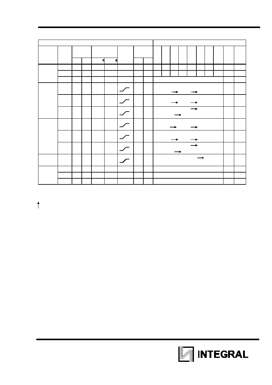
FUNCTION TABLE
Inputs Response
Mode Rese
t
Mode
Select
Output
Enables
Clock Serial
Inputs
P
A
/
Q
A
P
B
/
Q
B
P
C
/
Q
C
P
D
/
Q
D
P
E
/
Q
E
P
F
/
Q
F
P
G
/
Q
G
P
H
/
Q
H
Q
A
' Q
H
'
S
2
S
1
OE1 OE2
D
A
D
H
Reset L X L L L X X X L
L
L
L
L
L
L L L L
L
L
X
L
L
X
X
X
L
L
L
L
L
L
L
L
L
L
L
H
H
X
X
X
X
X Q
A
through Q
H
=Z L
L
Shift
Right
H
L H
H
X
D X Shift Right: Q
A
through Q
H
=Z;
D
A
F
A
; F
A
F
B
; etc
D Q
G
H
L H
X
H
D X Shift Right: Q
A
through Q
H
=Z;
D
A
F
A
; F
A
F
B
; etc
D Q
G
H
L H
L
L
D X
Shift Right: D
A
F
A
=Q
A
;
F
A
F
B
=Q
B
; etc
D Q
G
Shift
Left
H
H L
H
X
X D
Shift Left: Q
A
through Q
H
=Z;
D
H
F
H
; F
H
F
G
; etc
Q
B
D
H
H L
X
H
X D
Shift Left: Q
A
through Q
H
=Z;
D
H
F
H
; F
H
F
G
; etc
Q
B
D
H
H L
L
L
X D
Shift Left: D
H
F
H
=Q
H
;
F
H
F
G
=Q
G
; etc
Q
B
D
Parallel
Load
H H H X X X X Parallel
Load:P
N
F
N
P
A
P
H
Hold H L
L H X X X
X
Hold:
Q
A
through Q
H
=Z; F
N
=F
N
P
A
P
H
H
L
L
X
H
X
X
X
Hold:
Q
A
through Q
H
=Z; F
N
=F
N
P
A
P
H
H
L
L
L
L
X
X
X
Hold:
Q
N
=Q
H
P
A
P
H
Z = high impedance
D = data on serial input
F = flip-flop (see Logic Diagram)
When one or both output controls are high the eight input/output terminals are disabled to the
high-
impedance state; however, sequential operation or clearing of the register is not affected.