IN74HC03A
IN74HC03A
Quad 2-Input NAND Gate
with Open-Drain Outputs
High-Performance Silicon-Gate CMOS
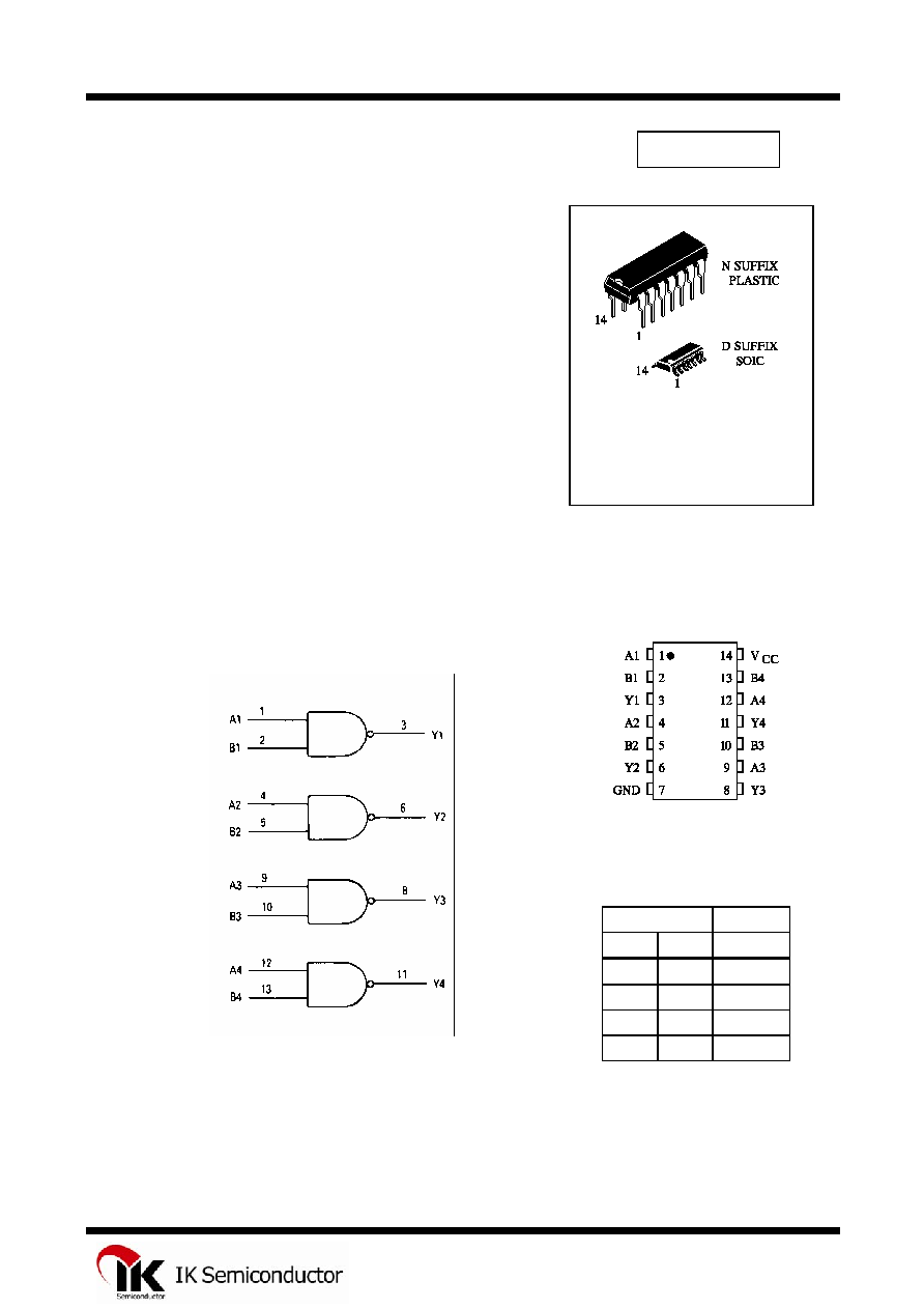
ORDERING INFORMATION
IN74HC03AN Plastic
IN74HC03AD SOIC
T
A
= -55
ú to 125ú C for all packages
The IN74HC03A is identical in pinout to the LS/ALS03. The device
inputs are compatible with standard CMOS outputs; with pullup resistors,
they are compatible with LS/ALSTTL outputs.
The IN74HC03A NAND gate has, as its output, a high-performance
MOS N-Channel transistor. This NAND gate can, therefore, with a
suitable pullup resistor, be used in wired-AND applications.
û
Outputs Directly Interface to CMOS, NMOS, and TTL
û
Operating Voltage Range: 2.0 to 6.0 V
û
Low Input Current: 1.0
A
û
High Noise Immunity Characteristic of CMOS Devices
PIN ASSIGNMENT
LOGIC DIAGRAM
PIN 14 =V
CC
PIN 7 = GND
FUNCTION TABLE
Inputs Output
A B Y
L L Z
L H Z
H L Z
H H L
Z= High Impedance
1
IN74HC03A
MAXIMUM RATINGS
*
Symbol Parameter
Value
Unit
V
CC
DC Supply Voltage (Referenced to GND)
-0.5 to +7.0
V
V
IN
DC Input Voltage (Referenced to GND)
-1.5 to V
CC
+1.5
V
V
OUT
DC Output Voltage (Referenced to GND)
-0.5 to V
CC
+0.5
V
I
IN
DC Input Current, per Pin
20
mA
I
OUT
DC Output Current, per Pin
25
mA
I
CC
DC Supply Current, V
CC
and GND Pins
50
mA
P
D
Power Dissipation in Still Air, Plastic DIP+
SOIC Package+
750
500
mW
Tstg
Storage Temperature
-65 to +150
úC
T
L
Lead Temperature, 1 mm from Case for 10 Seconds
(Plastic DIP or SOIC Package)
260
úC
*
Maximum Ratings are those values beyond which damage to the device may occur.
Functional operation should be restricted to the Recommended Operating Conditions.
+Derating - Plastic DIP: - 10 mW/
úC from 65ú to 125úC
SOIC Package: : - 7 mW/
úC from 65ú to 125úC
RECOMMENDED OPERATING CONDITIONS
Symbol Parameter Min
Max
Unit
V
CC
DC Supply Voltage (Referenced to GND)
2.0
6.0
V
V
IN
, V
OUT
DC Input Voltage, Output Voltage (Referenced to GND)
0
V
CC
V
T
A
Operating Temperature, All Package Types
-55
+125
úC
t
r
, t
f
Input Rise and Fall Time (Figure 1)
V
CC
=2.0 V
V
CC
=4.5 V
V
CC
=6.0 V
0
0
0
1000
500
400
ns
This device contains protection circuitry to guard against damage due to high static voltages or electric fields.
However, precautions must be taken to avoid applications of any voltage higher than maximum rated voltages to this
high-impedance circuit. For proper operation, V
IN
and V
OUT
should be constrained to the range GND
ò(V
IN
or
V
OUT
)
òV
CC
.
Unused inputs must always be tied to an appropriate logic voltage level (e.g., either GND or V
CC
). Unused
outputs must be left open.
2
IN74HC03A
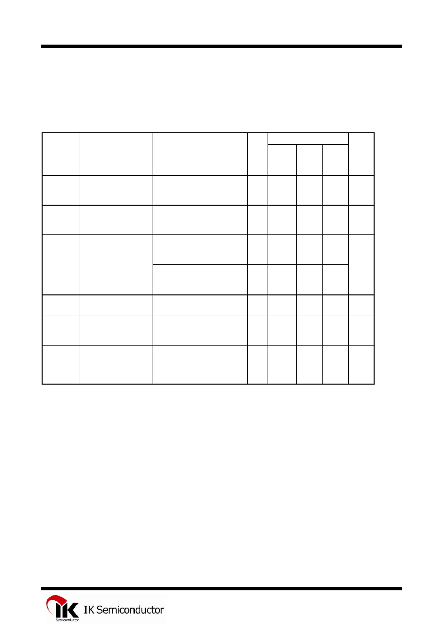
DC ELECTRICAL CHARACTERISTICS
(Voltages Referenced to GND)
V
CC
Guaranteed Limit
Symbol Parameter
Test
Conditions V
25
úC
to
-55
úC
ò85
úC
ò125
úC
Unit
V
IH
Minimum High-
Level Input Voltage
V
OUT
=0.1 V or V
CC
-0.1 V
I
OUT
ò 20 A
2.0
4.5
6.0
1.5
3.15
4.2
1.5
3.15
4.2
1.5
3.15
4.2
V
V
IL
Maximum Low -
Level Input Voltage
V
OUT
=0.1 V or V
CC
-0.1 V
I
OUT
ò 20 A
2.0
4.5
6.0
0.5
1.35
1.8
0.5
1.35
1.8
0.5
1.35
1.8
V
V
OL
Maximum Low-
Level Output Voltage
V
IN
=V
IH
I
OUT
ò 20 A
2.0
4.5
6.0
0.1
0.1
0.1
0.1
0.1
0.1
0.1
0.1
0.1
V
V
IN
=V
IH
I
OUT
ò 4.0 mA
I
OUT
ò 5.2 mA
4.5
6.0
0.26
0.26
0.33
0.33
0.4
0.4
I
IN
Maximum Input
Leakage Current
V
IN
=V
CC
or GND
6.0
0.1
1.0
1.0
A
I
CC
Maximum Quiescent
Supply Current
(per Package)
V
IN
=V
CC
or GND
I
OUT
=0
A
6.0
1.0 10 40
A
I
OZ
Maximum Three-
State Leakage
Current
Output in High-Impedance
State
V
IN
= V
IL
or V
IH
I
OUT
= V
CC
or GND
6.0
0.5
5.0
10
A
3
IN74HC03A
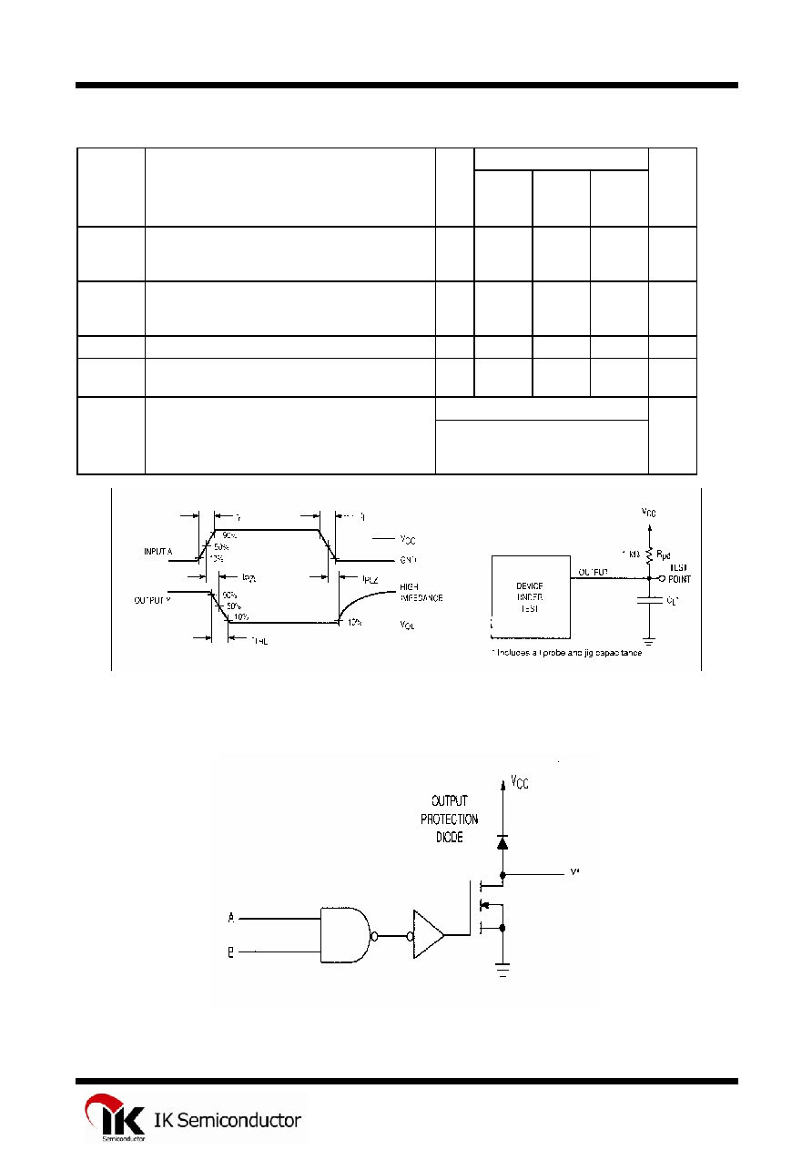
AC ELECTRICAL CHARACTERISTICS (CL=50pF,Input tr=tf=6.0 ns)
V
CC
Guaranteed Limit
Symbol Parameter V
25
úC
to
-55
úC
ò85úC ò125úC Unit
t
PLZ
, t
PZL
Maximum Propagation Delay, Input A or B to
Output Y (Figures 1 and 2)
2.0
4.5
6.0
120
24
20
150
30
26
180
36
31
ns
t
THL
Maximum Output Transition Time, Any Output
(Figures 1 and 2)
2.0
4.5
6.0
75
15
13
95
19
16
110
22
19
ns
C
IN
Maximum Input Capacitance
-
10
10
10
pF
C
OUT
Maximum Three-State Output Capacitance
(Output in High-Impedance State)
- 10 10 10 pF
Power Dissipation Capacitance (Per Gate)
Typical @25
úC,V
CC
=5.0 V
C
PD
Used to determine the no-load dynamic power
consumption:
P
D
=C
PD
V
CC
2
f+I
CC
V
CC
8.0 pF
.Figure 1. Switching Waveforms
Figure 2. Test Circuit
EXPANDED LOGIC DIAGRAM
(1/4 of the Device)
*
Denotes open-drain outputs
4
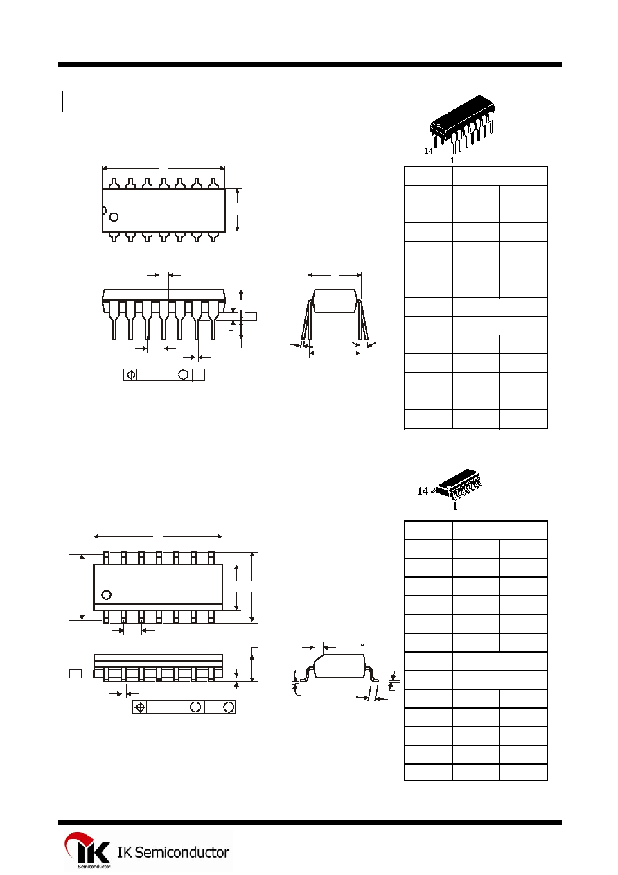
IN74HC03A
N SUFFIX PLASTIC DIP
(MS - 001AA)
Symbol
MIN
MAX
A
18.67
19.69
B
6.1
7.11
C
5.33
D
0.36
0.56
F
1.14
1.78
G
H
J
0
ú
10
ú
K
2.92
3.81
NOTES:
L
7.62
8.26
1.
Dimensions "A", "B" do not include mold flash or protrusions.
M
0.2
0.36
Maximum mold flash or protrusions 0.25 mm (0.010) per side.
N
0.38
D SUFFIX SOIC
(MS - 012AB)
Symbol
MIN
MAX
A
8.55
8.75
B
3.8
4
C
1.35
1.75
D
0.33
0.51
F
0.4
1.27
G
H
J
0ú
8ú
NOTES:
K
0.1
0.25
1.
Dimensions A and B do not include mold flash or protrusion.
M
0.19
0.25
2.
Maximum mold flash or protrusion 0.15 mm (0.006) per side
P
5.8
6.2
for A; for B 0.25 mm (0.010) per side.
R
0.25
0.5
Dimension, mm
1.27
5.27
2.54
7.62
Dimension, mm
A
B
H
C
K
C M
J
F
M
P
G
D
R x 45
SEATING
PLANE
0.25 (0.010) M T
-T-
1
14
7
8
A
B
F
G
D
L
H
SEATING
PLANE
N
K
0.25 (0.010) M T
M
J
-T-
C
1
14
7
8
5