TECHNICAL DATA
1
INTEGRAL
Quad 2-Input Data Selectors/Multiplexer
The IN74HC157A is identical in pin out to the LS/ALS157. The device
inputs are compatible with standard CMOS outputs; with pull up resistors,
they are compatible with LS/ALSTTL outputs.
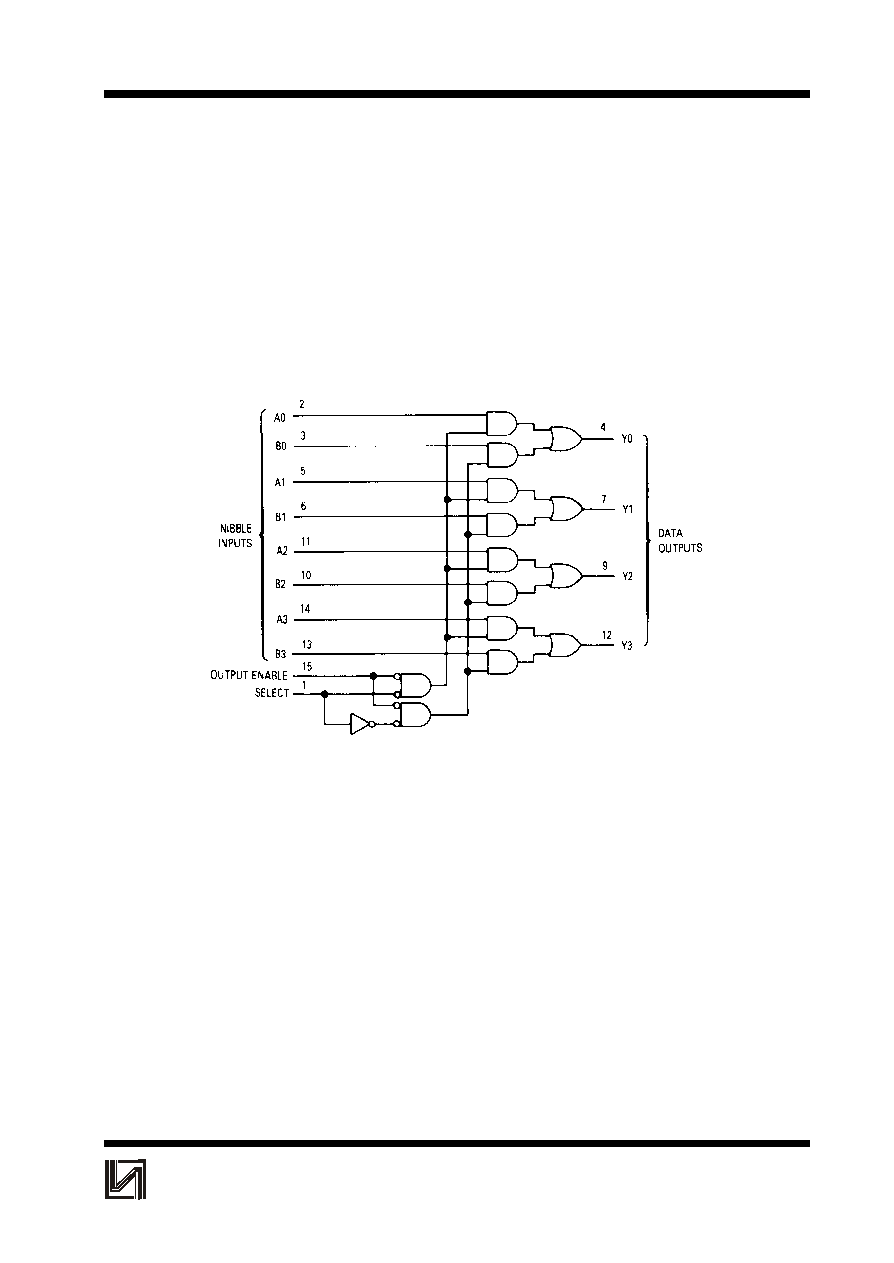
This device routes 2 nibbles (A or B) to a single port (Y) as determined
by the Select input. The data is presented at the outputs in non inverted
form. A high level on the Output Enable input sets all four Y outputs to a low
level.
û
Outputs Directly Interface to CMOS, NMOS, and TTL
û
Operating Voltage Range: 2.0 to 6.0 V
û
Low Input Current: 1.0
A
û
High Noise Immunity Characteristic of CMOS Devices
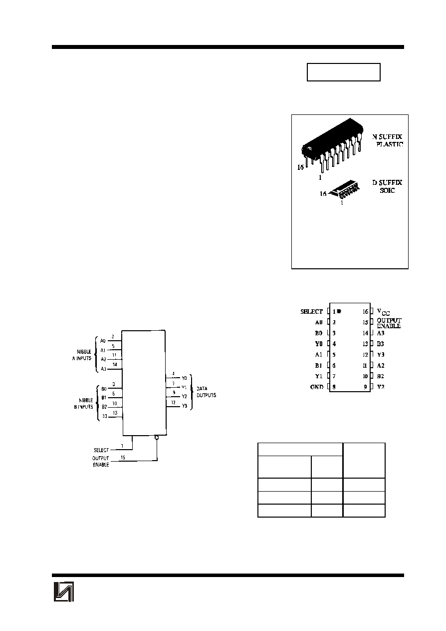
IN74HC157A
ORDERING INFORMATION
IN74HC157AN Plastic
IN74HC157AD SOIC
IZ74HC157A Chip
T
A
= -55
ú
to 125
ú
C for all packages
PIN ASSIGNMENT
FUNCTION TABLE
Inputs
Outputs
Output
Enable
Select
Y0-Y3
H
X
L
L
L
A0-A3
L
H
B0-B3
X=don't care
A0-A3, B0-B3=the levels of the respective
Data-Word Inputs
LOGIC DIAGRAM
PIN 16 =V
CC
PIN 8 = GND
IN74HC157A
2
INTEGRAL
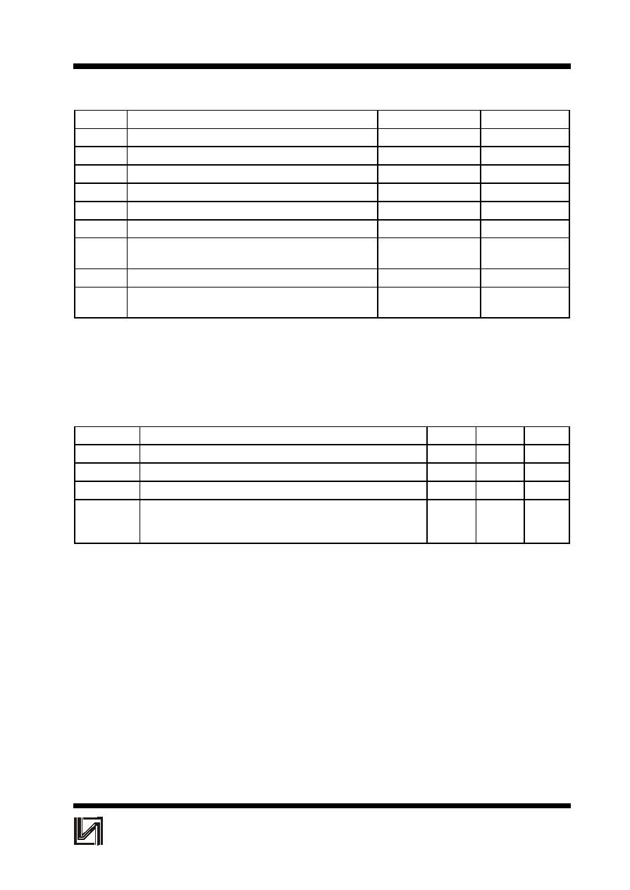
MAXIMUM RATINGS
*
Symbol
Parameter
Value
Unit
V
CC
DC Supply Voltage (Referenced to GND)
-0.5 to +7.0
V
V
IN
DC Input Voltage (Referenced to GND)
-1.5 to V
CC
+1.5
V
V
OUT
DC Output Voltage (Referenced to GND)
-0.5 to V
CC
+0.5
V
I
IN
DC Input Current, per Pin
20
mA
I
OUT
DC Output Current, per Pin
25
mA
I
CC
DC Supply Current, V
CC
and GND Pins
50
mA
P
D
Power Dissipation in Still Air, Plastic DIP
**
SOIC Package
**
750
500
mW
Tstg
Storage Temperature
-65 to +150
ú
C
T
L
Lead Temperature, 1 mm from Case for 10 Seconds
(Plastic DIP or SOIC Package)
260
ú
C
*
Maximum Ratings are those values beyond which damage to the device may occur.
Functional operation should be restricted to the Recommended Operating Conditions.
**
Derating - Plastic DIP: - 10 mW/
ú
C from 65
ú
to 125
ú
C
SOIC Package: : - 7 mW/
ú
C from 65
ú
to 125
ú
C
RECOMMENDED OPERATING CONDITIONS
Symbol
Parameter
Min
Max
Unit
V
CC
DC Supply Voltage (Referenced to GND)
2.0
6.0
V
V
IN
, V
OUT
DC Input Voltage, Output Voltage (Referenced to GND)
0
V
CC
V
T
A
Operating Temperature, All Package Types
-55
+125
ú
C
t
r
, t
f
Input Rise and Fall Time (Figure 1)
V
CC
=2.0 V
V
CC
=4.5 V
V
CC
=6.0 V
0
0
0
1000
500
400
ns
This device contains protection circuitry to guard against damage due to high static voltages or electric
fields. However, precautions must be taken to avoid applications of any voltage higher than maximum rated voltages
to this high-impedance circuit. For proper operation, V
IN
and V
OUT
should be constrained to the range GND
ò
(V
IN
or
V
OUT
)
ò
V
CC
.
Unused inputs must always be tied to an appropriate logic voltage level (e.g., either GND or V
CC
). Unused
outputs must be left open.
IN74HC157A
3
INTEGRAL
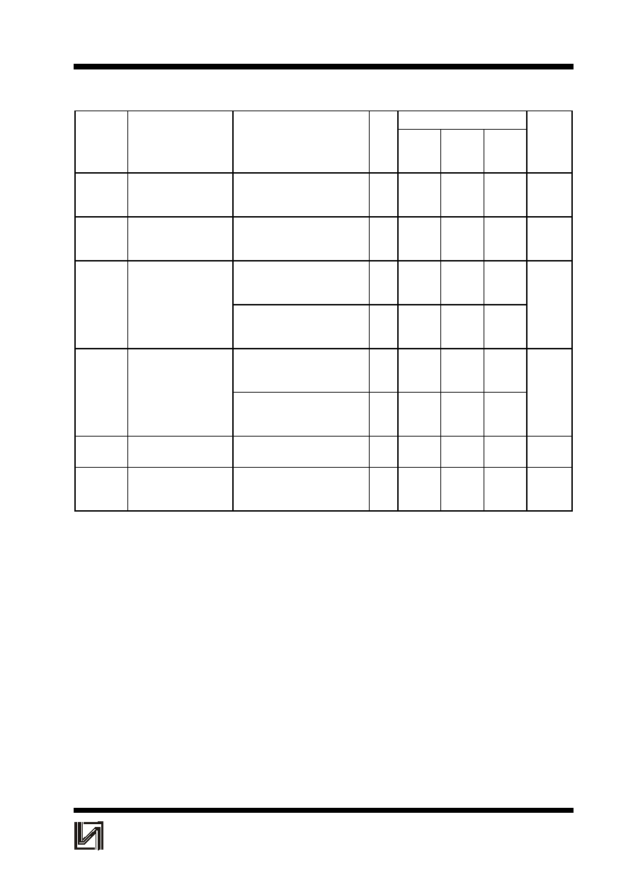
DC ELECTRICAL CHARACTERISTICS
(Voltages Referenced to GND)
Guaranteed Limit
Symbol
Parameter
Test Conditions
V
CC
V
25
ú
C
to
-55
ú
C
ò
85
ú
C
ò
125
ú
C
Unit
V
IH
Minimum High-Level
Input Voltage
V
OUT
=0.1 V or V
CC
-0.1 V
I
OUT
ò
20
A
2.0
4.5
6.0
1.5
3.15
4.2
1.5
3.15
4.2
1.5
3.15
4.2
V
V
IL
Maximum Low -Level
Input Voltage
V
OUT
=0.1 V or V
CC
-0.1 V
I
OUT
ò
20
A
2.0
4.5
6.0
0.5
1.35
1.8
0.5
1.35
1.8
0.5
1.35
1.8
V
V
OH
Minimum High-Level
Output Voltage
V
IN
=V
IH
or V
IL
I
OUT
ò
20
A
2.0
4.5
6.0
1.9
4.4
5.9
1.9
4.4
5.9
1.9
4.4
5.9
V
V
IN
=V
IH
or V
IL
I
OUT
ò
4.0 mA
I
OUT
ò
5.2 mA
4.5
6.0
3.98
5.48
3.84
5.34
3.7
5.2
V
OL
Maximum Low-Level
Output Voltage
V
IN
=V
IH
or V
IL
I
OUT
ò
20
A
2.0
4.5
6.0
0.1
0.1
0.1
0.1
0.1
0.1
0.1
0.1
0.1
V
V
IN
=V
IH
or V
IL
I
OUT
ò
4.0 mA
I
OUT
ò
5.2 mA
4.5
6.0
0.26
0.26
0.33
0.33
0.4
0.4
I
IN
Maximum Input
Leakage Current
V
IN
=V
CC
or GND
6.0
0.1
1.0
1.0
A
I
CC
Maximum Quiescent
Supply Current
(per Package)
V
IN
=V
CC
or GND
I
OUT
=0
A
6.0
4.0
40
160
A
IN74HC157A
4
INTEGRAL
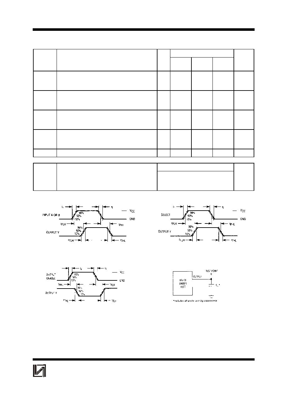
AC ELECTRICAL CHARACTERISTICS
(C
L
=50pF,Input t
r
=t
f
=6.0 ns)
V
CC
Guaranteed Limit
Symbol
Parameter
V
25
ú
C to
-55
ú
C
ò
85
ú
C
ò
125
ú
C
Unit
t
PLH
, t
PHL
Maximum Propagation Delay, Input A or B to
Output Y (Figures 1and 4)
2.0
4.5
6.0
105
21
18
130
26
22
160
32
27
ns
t
PLH
, t
PHL
Maximum Propagation Delay , Select to
Output Y (Figures 2 and 4)
2.0
4.5
6.0
110
22
19
140
28
24
165
33
28
ns
t
PLH
, t
PHL
Maximum Propagation Delay , Output Enable to
Output Y (Figures 3 and 4)
2.0
4.5
6.0
100
20
17
125
25
21
150
30
26
ns
t
TLH
, t
THL
Maximum Output Transition Time, Any Output
(Figures 1 and 4)
2.0
4.5
6.0
75
15
13
95
19
16
110
22
19
ns
C
IN
Maximum Input Capacitance
-
10
10
10
pF
Power Dissipation Capacitance (Per Package)
Typical @25
ú
C,V
CC
=5.0 V
C
PD
Used to determine the no-load dynamic power
consumption:
P
D
=C
PD
V
CC
2
f+I
CC
V
CC
33
pF
Figure 1. Switching Waveforms
Figure 2. Switching Waveforms
Figure 3. Switching Waveforms
Figure 4. Test Circuit
IN74HC157A
5
INTEGRAL
EXPANDED LOGIC DIAGRAM