
TECHNICAL DATA
235
8-Bit Serial or Parallel-Input/
Serial-Output Shift Register
High-Performance Silicon-Gate CMOS
The IN74HC166 is identical in pinout to the LS/ALS166. The
device inputs are compatible with standard CMOS outputs; with pullup
resistors, they are compatible with LS/ALSTTL outputs.
This device is a parallel-in or serial-in, serial-out shift register with
gated clock inputs and an overriding clear input. The shift/load input
establishes the parallel-in or serial-in mode. When high, this input
enables the serial data input and couples the eight flip-flops for serial
shifting with each clock pulse. Synchronous loading occurs on the next
clock pulse when this is low and the parallel data inputs are enabled.
Serial data flow is inhibited during parallel loading. Clocking is done
on the low-to-high level edge of the clock pulse via a two input
positive NOR gate, which permits one input to be used as a clock
enable or clock inhibit function. Clocking is inhibited when either of
the clock inputs are held high, holding either input low enables the
other clock input. This will allow the system clock to be free running
and the register stopped on command with the other clock input. A
change from low-to-high on the clock inhibit input should only be
done when the clock input is high. A buffered direct clear input
overrides all other inputs, including the clock, andsets all flip-flop to
zero.
û
Outputs Directly Interface to CMOS, NMOS, and TTL
û
Operating Voltage Range: 2.0 to 6.0 V
û
Low Input Current: 1.0
A
û
High Noise Immunity Characteristic of CMOS Devices
IN74HC166
ORDERING INFORMATION
IN74HC166N Plastic
IN74HC166D SOIC
T
A
= -55
ú
to 125
ú
C for all packages
PIN ASSIGNMENT
LOGIC DIAGRAM
PIN 16 =V
CC
PIN 8 = GND
IN74HC166
236
MAXIMUM RATINGS
*
Symbol
Parameter
Value
Unit
V
CC
DC Supply Voltage (Referenced to GND)
-0.5 to +7.0
V
V
IN
DC Input Voltage (Referenced to GND)
-1.5 to V
CC
+1.5
V
V
OUT
DC Output Voltage (Referenced to GND)
-0.5 to V
CC
+0.5
V
I
IN
DC Input Current, per Pin
20
mA
I
OUT
DC Output Current, per Pin
25
mA
I
CC
DC Supply Current, V
CC
and GND Pins
50
mA
P
D
Power Dissipation in Still Air, Plastic DIP+
SOIC Package+
750
500
mW
Tstg
Storage Temperature
-65 to +150
ú
C
T
L
Lead Temperature, 1 mm from Case for 10 Seconds
(Plastic DIP or SOIC Package)
260
ú
C
*
Maximum Ratings are those values beyond which damage to the device may occur.
Functional operation should be restricted to the Recommended Operating Conditions.
+Derating - Plastic DIP: - 10 mW/
ú
C from 65
ú
to 125
ú
C
SOIC Package: : - 7 mW/
ú
C from 65
ú
to 125
ú
C
RECOMMENDED OPERATING CONDITIONS
Symbol
Parameter
Min
Max
Unit
V
CC
DC Supply Voltage (Referenced to GND)
2.0
6.0
V
V
IN
, V
OUT
DC Input Voltage, Output Voltage (Referenced to GND)
0
V
CC
V
T
A
Operating Temperature, All Package Types
-55
+125
ú
C
t
r
, t
f
Input Rise and Fall Time (Figure 1)
V
CC
=2.0 V
V
CC
=4.5 V
V
CC
=6.0 V
0
0
0
1000
500
400
ns
This device contains protection circuitry to guard against damage due to high static voltages or electric
fields. However, precautions must be taken to avoid applications of any voltage higher than maximum rated
voltages to this high-impedance circuit. For proper operation, V
IN
and V
OUT
should be constrained to the range
GND
ò
(V
IN
or V
OUT
)
ò
V
CC
.
Unused inputs must always be tied to an appropriate logic voltage level (e.g., either GND or V
CC
).
Unused outputs must be left open.
IN74HC166
237
DC ELECTRICAL CHARACTERISTICS
(Voltages Referenced to GND)
V
CC
Guaranteed Limit
Symbol
Parameter
Test Conditions
V
25
ú
C
to
-55
ú
C
ò
85
ú
C
ò
125
ú
C
Unit
V
IH
Minimum High-Level
Input Voltage
V
OUT
=0.1 V or V
CC
-0.1 V
I
OUT
ò
20
A
2.0
4.5
6.0
1.5
3.15
4.2
1.5
3.15
4.2
1.5
3.15
4.2
V
V
IL
Maximum Low -
Level Input Voltage
V
OUT
=0.1 V or V
CC
-0.1 V
I
OUT
ò
20
A
2.0
4.5
6.0
0.3
0.9
1.2
0.3
0.9
1.2
0.3
0.9
1.2
V
V
OH
Minimum High-Level
Output Voltage
V
IN
=V
IH
or V
IL
I
OUT
ò
20
A
2.0
4.5
6.0
1.9
4.4
5.9
1.9
4.4
5.9
1.9
4.4
5.9
V
V
IN
=V
IH
or V
IL
I
OUT
ò
4.0 mA
I
OUT
ò
5.2 mA
4.5
6.0
3.98
5.48
3.84
5.34
3.7
5.2
V
OL
Maximum Low-Level
Output Voltage
V
IN
=V
IH
or V
IL
I
OUT
ò
20
A
2.0
4.5
6.0
0.1
0.1
0.1
0.1
0.1
0.1
0.1
0.1
0.1
V
V
IN
=V
IH
or V
IL
I
OUT
ò
4.0 mA
I
OUT
ò
5.2 mA
4.5
6.0
0.26
0.26
0.33
0.33
0.4
0.4
I
IN
Maximum Input
Leakage Current
V
IN
=V
CC
or GND
6.0
0.1
1.0
1.0
A
I
CC
Maximum Quiescent
Supply Current
(per Package)
V
IN
=V
CC
or GND
I
OUT
=0
A
6.0
8.0
80
160
A
FUNCTION TABLE
Inputs
Internal
Outputs
Output
Clear
Shift/Load
Clock
Inhibit
Clock
S
A
Parallel
A...H
Q
A
Q
B
Q
H
L
X
X
X
X
X
L
L
L
H
X
X
X
X
No change
H
L
L
X
a...h
a
b
h
H
H
L
H
X
H
Q
An
Q
Gn
H
H
L
L
X
L
Q
An
Q
Gn
H
X
H
X
X
X
No change
X = don't care
a...h = the level of steady state input voltage at input A trough H respectively
IN74HC166
238
AC ELECTRICAL CHARACTERISTICS
(C
L
=50pF,Input t
r
=t
f
=6.0 ns)
V
CC
Guaranteed Limit
Symbol
Parameter
V
25
ú
C
to
-55
ú
C
ò
85
ú
C
ò
125
ú
C
Unit
f
max
Minimum Clock Frequency (50% Duty Cycle)
(Figures 2 and 4)
2.0
4.5
6.0
6.0
31
36
5.0
25
28
4.2
21
25
MHz
t
PLH
, t
PHL
Maximum Propagation Delay, Clock (or Clock
Inhibit) to Q
H
(Figures 2,3 and 4)
2.0
4.5
6.0
140
28
24
175
35
30
210
42
36
ns
t
PHL
Maximum Propagation Delay , Clear to Q
H
(Figures 1 and 4)
2.0
4.5
6.0
150
30
26
200
40
34
230
48
40
ns
t
TLH
, t
THL
Maximum Output Transition Time, Any Output
(Figures 1 and 4)
2.0
4.5
6.0
75
16
14
95
20
18
110
25
20
ns
C
IN
Maximum Input Capacitance
-
10
10
10
pF
Power Dissipation Capacitance (Per Package)
Typical @25
ú
C,V
CC
=5.0 V
C
PD
Used to determine the no-load dynamic power
consumption:
P
D
=C
PD
V
CC
2
f+I
CC
V
CC
140
pF
TIMING REQUIREMENTS
(C
L
=50pF,Input t
r
=t
f
=6.0 ns)
V
CC
Guaranteed Limit
Symbol
Parameter
V
25
ú
C to
-55
ú
C
ò
85
ú
C
ò
125
ú
C
Unit
t
su
Minimum Setup Time, Shift/Load to
Clock (Figure 3)
2.0
4.5
6.0
80
16
14
100
20
18
120
24
20
ns
t
su
Minimum Setup Time, Data before
Clock (or Clock Inhibit) (Figure 3)
2.0
4.5
6.0
80
16
14
100
20
18
120
24
20
ns
t
w
Minimum Pulse Width, Clock (or
Clock Inhibit) (Figure 2)
2.0
4.5
6.0
80
16
14
100
20
17
120
24
20
ns
IN74HC166
239
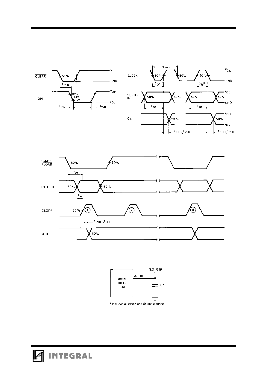
Figure 1. Switching Waveforms
Figure 2. Switching Waveforms
Figure 3. Switching Waveforms
Figure 4. Test Circuit