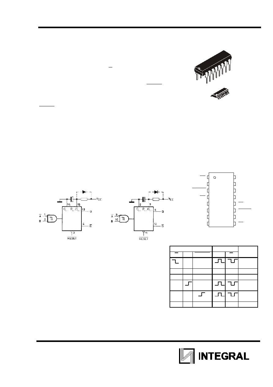
IN74HC221A
1
D
UAL
M
ONOSTABLE
M
ULTIVIBRATOR
The IN74HC221A is identical in pinout to the LS/ALS221. The
device inputs are compatible with standard CMOS outputs; with
pullup resistors, they are compatible with LS/ALSTTL outputs.
There are two trigger inputs, A INPUT (negative edge) and
B INPUT (positive edge). These inputs are valid for rising/falling
signals
The device may also be triggered by using the RESET input
(positive-edge) because of the Schmitt-trigger input; after
triggering the output maintains the MONOSTABLE state for the
time period determined by the external resistor R
EXT
and
capacitor C
EXT
. Taking RESET low breaks this MONOSTABLE
STATE. If the next trigger pulse occurs during the
MONOSTABLE period it makes the MONOSTABLE period
longer.
û Outputs Directly Interface to CMOS, NMOS, and TTL
û Operating Voltage Range: 3.0 to 6.0 V
û Low Input Current: 1.0 A
û High Noise Immunity Characteristic of CMOS Devices
N SUFFIX
PLASTIC
D SUFFIX
SOIC
1
16
1
16
ORDERING INFORMATION
IN74HC221AN Plastic
IN74HC221AD SOIC
IZ74HC221AZ Chip
T
A
= -55
ú to 125ú C for all
packages
PIN ASSIGNMENT
Note
(1) C
EXT
, R
EXT
, D
EXT
are external components.
(2) D
EXT
is a clamping diode.
The external capacitor is charged to V
CC
in the stand-by
state, i.e. no trigger. When the supply voltage is turned off
C
X
is discharged mainly through an internal parasitic
diode. If C
X
is sufficiently large and V
CC
decreases rapidy,
there will be some possibility of damaging the I.C. with a
surge current or latch-up. If the voltage supply filter
capacitor is large enough and V
CC
decrease slowly, the
surge current is automatically limited and damage the I.C.
is avoided. The maximum forward current of the parasitic
diode is approximately 20 mA.
LOGIC DIAGRAM
PIN 16 =V
CC
PIN 8 = GND
FUNCTION TABLE
Inputs Outputs
Note
A B
RESET
Q Q
H H Output
Enable
X L H L
*
H
*
Inhibit
H X H L
*
H
*
Inhibit
L H Output
Enable
L H
Output
Enable
X X L
L H Inhibit
X = don't care
*
- except for monostable period
1
2
3
5
4
6
7
8
16
15
14
13
12
11
10
9
GND
VCC
1R /C
EXT
EXT
1C
EXT
1Q
2Q
2RESET
2B
2A
1A
1B
1RESET
1Q
2Q
2C
EXT
2R /C
EXT
EXT
C
EXT
R
EXT
D
EXT
C
EXT
R
EXT
D
EXT
IN74HC221A
2
MAXIMUM RATINGS
*
Symbol Parameter
Value
Unit
V
CC
DC Supply Voltage (Referenced to GND)
-0.5 to +7.0
V
V
IN
DC Input Voltage (Referenced to GND)
-1.5 to V
CC
+1.5
V
V
OUT
DC Output Voltage (Referenced to GND)
-0.5 to V
CC
+0.5
V
I
IN
DC Input Current, per Pin
A ,
B
,
RESET
C
EXT
, R
EXT
20
30
mA
I
OUT
DC Output Current, per Pin
25
mA
I
CC
DC Supply Current, V
CC
and GND Pins
50
mA
P
D
Power Dissipation in Still Air, Plastic DIP
**
SOIC Package
**
750
500
mW
Tstg
Storage Temperature
-65 to +150
úC
T
L
Lead Temperature, 1 mm from Case for 10
Seconds
(Plastic DIP or SOIC Package)
260
úC
*
Maximum Ratings are those values beyond which damage to the device may occur.
Functional operation should be restricted to the Recommended Operating Conditions.
**
Derating - Plastic DIP: - 10 mW/
úC from 65ú to 125úC
SOIC Package: : - 7 mW/
úC from 65ú to 125úC
RECOMMENDED OPERATING CONDITIONS
Symbol Parameter Min
Max
Unit
V
CC
DC Supply Voltage (Referenced to GND)
3.0
*
6.0 V
V
IN
, V
OUT
DC Input Voltage, Output Voltage (Referenced to
GND)
0 V
CC
V
T
A
Operating Temperature, All Package Types
-55
+125
úC
Input Rise and Fall Time -
RESET
(Figure 2)
V
CC
=2.0 V
V
CC
=4.5 V
V
CC
=6.0 V
0
0
0
1000
500
400
t
r
, t
f
A A or
B
-
No
Limit
ns
R
X
External Timing Resistor
V
CC
<4.5 V
V
CC
ô 4.5 V
10
2.0
1000
1000
k
C
X
External Timing Capacitor
0
No
Limit
F
*
The IN74HC221 will function at 2.0 V but for optimum pulse width stability, V
CC
should be above
3.0 V.
This device contains protection circuitry to guard against damage due to high static
voltages or electric fields. However, precautions must be taken to avoid applications of any voltage
higher than maximum rated voltages to this high-impedance circuit. For proper operation, V
IN
and
V
OUT
should be constrained to the range GND
ò(V
IN
or V
OUT
)
òV
CC
.
Unused inputs must always be tied to an appropriate logic voltage level (e.g., either GND or
V
CC
). Unused outputs must be left open.
IN74HC221A
3
DC ELECTRICAL CHARACTERISTICS(Voltages Referenced to GND)
Guaranteed Limit
Symbol Parameter Test
Conditions
V
CC
V
-55
úC
to
25
úC
ò85
úC
ò125
úC
Unit
V
IL
Maximum Low -
Level Input Voltage
V
OUT
ò 0.1 V or
V
CC
=0.1 V
I
OUT
ò 20 A
2.0
4.5
6.0
0.3
0.9
1.2
0.3
0.9
1.2
0.3
0.9
1.2
V
V
IH
Minimum
High-Level
Input Voltage
V
OUT
ò 0.1 V or
V
CC
=0.1 V
I
OUT
ò 20 A
2.0
4.5
6.0
1.5
3.15
4.2
1.5
3.15
4.2
1.5
3.15
4.2
V
V
IN
=V
IH
or V
IL
I
OUT
ò 20 A
2.0
4.5
6.0
0.1
0.1
0.1
0.1
0.1
0.1
0.1
0.1
0.1
V
IN
=V
IH
or V
IL
I
OUT
ò 4.0 mA
4.5
0.26
0.33
0.4
V
OL
Maximum
Low-Level
Output Voltage
V
IN
=V
IH
or V
IL
I
OUT
ò 5.2 mA
6.0 0.26 0.33 0.40
V
V
IN
=V
IH
or V
IL
I
OUT
ò -20 A
2.0
4.5
6.0
1.9
4.4
5.9
1.9
4.4
5.9
1.9
4.4
5.9
V
IN
=V
IH
or V
IL
I
OUT
ò -4.0 mA
4.5 3.98 3.84 3.70
V
OH
Minimum High-
Level Output
Voltage
V
IN
=V
IH
or V
IL
I
OUT
ò -5.2 mA
6.0 5.48 5.34 5.2
V
I
IL
Maximum Low-
Level Output
Current
V
IL
=GND
V
IH
=V
CC
6.0 -0.1 -1.0 -1.0 A
I
IH
Minimum High-
Level Input Current
V
IL
=GND
V
IH
=V
CC
6.0 0.1 1.0 1.0 A
I
CC
Maximum
Quiescent Supply
Current (per
Package) Standby
State
V
IL
=GND
V
IÕ
=V
CC
I
OUT
=0
A
6.0 8.0 80 160 A
I
CC1
Maximum
Supply
Current (per
Package) Active
State
V
IL
=GND
V
IH
=V
CC
I
OUT
=0
A
V
IN
= 0.5 V
CC
2.0
4.5
6.0
0.08
1.0
2.0
0.11
1.3
2.6
0.13
1.6
3.2
mA
IN74HC221A
4
AC ELECTRICAL CHARACTERISTICS
Guaranteed Limit
Symbol
Parameter Test
Conditions
V
CC
V
-55
úC
to
25
úC
ò85
úC
ò125
úC
Unit
A, B -
Q
2.0
4.5
6.0
180
36
31
225
45
38
270
54
46
RESET - Q
2.0
4.5
6.0
180
36
31
225
45
38
270
54
46
t
PHL
Maximum
Propagation
Delay
RESET -
Q
V
IL
=0 V
V
IH
=V
CC
t
LH
=t
HL
=6 ns
C
L
=50 pF
C
EXT
=0
R
EXT
=5 k
2.0
4.5
6.0
195
39
33
245
49
42
295
59
50
ns
A, B - Q
2.0
4.5
6.0
220
44
37
275
55
47
330
66
56
RESET - Q
2.0
4.5
6.0
245
49
42
305
61
52
370
74
63
t
PLH
Maximum
Propagation
Delay
RESET -
Q
V
IL
=0 V
V
IH
=V
CC
t
LH
=t
HL
=6 ns
C
L
=50 pF
C
EXT
=0
R
EXT
=5 k
2.0
4.5
6.0
200
40
34
250
50
43
300
60
51
ns
t
TLH
, t
THL
Maximum Output Transition
Time, Any Output(Figures 2
and 3)
V
IL
=0 V
V
IH
=V
CC
t
LH
=t
HL
=6 ÌÒ
C
L
=50 pF
2.0
4.5
6.0
75
16
14
95
20
17
110
22
20
ns
C
IN
Maximum
Input
Capacitance
A
, B,
RESET
C
X
, R
X
-
10
20
10
20
10
20
pF
Power Dissipation
Capacitance
(Per Multivibrator)
C
PD
P
D
=C
PD
V
CC
2
f+I
CC
V
CC
5.0
180
*
pF
t
rec
Minimum Recovery Time,
Inactive to A or B
(Figure 2)
V
IL
=0 V
V
IH
=V
CC
t
LH
=t
HL
=6 ÌÒ
C
L
=50 pF
2.0
4.5
6.0
100
20
17
125
25
21
150
30
26
ns
A,
RESET
2.0
4.5
6.0
25
9
7
95
19
16
110
22
19
t
w
Minimum
Pulse Width
B
V
IL
=0 V
V
IH
=V
CC
t
LH
=t
HL
=6 ns
C
L
=50 pF
C
EXT
=0
R
EXT
=5 k
2.0
4.5
6.0
30
11
9
115
23
20
135
27
23
ns
—
EXT
=0 Ô‘
R
EXT
=5 k
5.0 105
*
ns
—
EXT
=1 nF
R
EXT
=10 k
2.0
4.5
6.0
0.80
*
0.75
*
0.70
*
t
WQ
Minimum Pulse Width
(Figure 4)
—
EXT
=1
F
R
EXT
=10 k
2.0
4.5
6.0
80
*
75
*
70
*
s
*
“
¿
=2510
úC
IN74HC221A
5
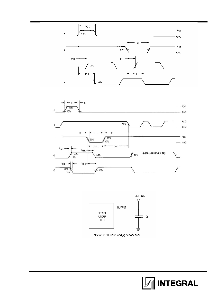
Figure 1. Switching Waveforms
Figure 2. Switching Waveforms
Figure 3. Test Circuit
RESET