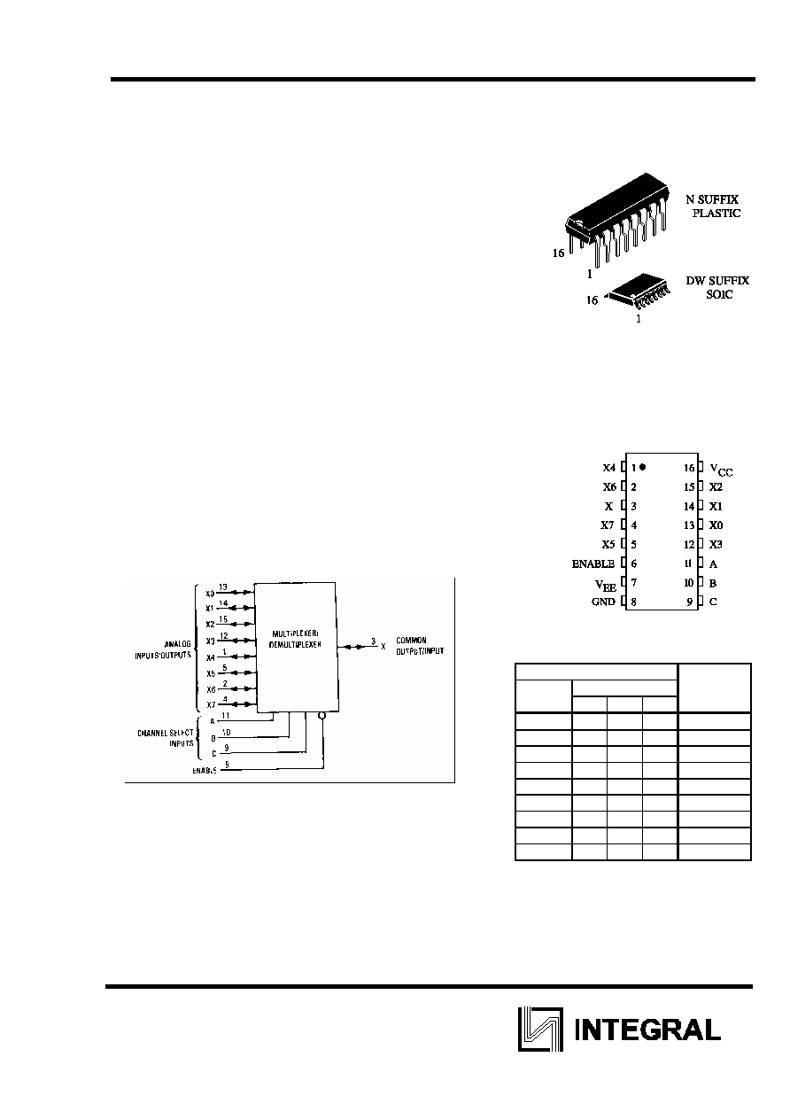
IN74HC4051
1
A
NALOG
M
ULTIPLEXER
D
EMULTIPLEXER
High-Performance Silicon-Gate CMOS
The IN74HC4051 utilize silicon-gate CMOS technology to
achieve fast propagation delays, low ON resistances, and low
OFF leakage currents. These analog multiplexers/demultiplexers
control analog voltages that may vary across the complete power
supply range (from V
CC
to V
EE
).
The Channel-Select inputs determine which one of the Analog
Inputs/Outputs is to be connected, by means of an analog
switch, to the Common Output/Input.When the Enable pin is
high, all analog switches are turned off.
The Channel-Select and Enable inputs are compatible with
standard CMOS outputs; with pullup resistors, they are
compatible with LS/ALSTTL outputs.
� Fast Switching and Propagation Speeds
� Low Crosstalk Between Switches
� Diode Protection on All Inputs/Outputs
� Analog Power Supply Range (V
CC
-V
EE
)=2.0 to 12.0 V
� Digital (Control) Power Supply Range (V
CC
-GND)=2.0 to 6.0 V
� Low Noise
ORDERING INFORMATION
IN74HC4051N Plastic
IN74HC4051DW SOIC
T
A
= -55
� to 125� C for all
packages
PIN ASSIGNMENT
FUNCTION TABLE
Control Inputs
ON
Enable Select Channels
C
B
A
L L L L X0
L L
L
H X1
L L H L
X2
L L
H
H X3
L H
L
L X4
L H L H X5
L H
H
L X6
L H H H
X7
H X X X None
X = don't care
LOGIC DIAGRAM
Single-Pole, 8-Position Plus Common Off
PIN 16 =V
CC
PIN 7 = V
EE
PIN 8 = GND
IN74HC4051
2
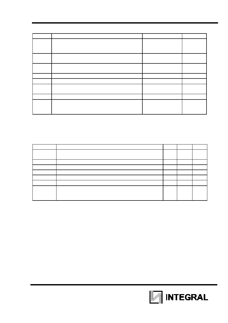
MAXIMUM RATINGS
*
Symbol Parameter
Value
Unit
V
CC
Positive DC Supply Voltage (Referenced to
GND)
(Referenced to V
EE
)
-0.5 to +7.0
-0.5 to +14.0
V
V
EE
Negative DC Supply Voltage (Referenced to
GND)
-7.0 to +0.5
V
V
IS
Analog Input Voltage
V
EE
- 0.5 to
V
CC
+0.5
V
V
IN
Digital Input Voltage (Referenced to GND)
-1.5 to V
CC
+1.5
V
I
DC Input Current Into or Out of Any Pin
25
mA
P
D
Power Dissipation in Still Air, Plastic DIP+
SOIC Package+
750
500
mW
Tstg
Storage Temperature
-65 to +150
�C
T
L
Lead Temperature, 1 mm from Case for 10
Seconds
(Plastic DIP or SOIC Package)
260
�C
*
Maximum Ratings are those values beyond which damage to the device may occur.
Functional operation should be restricted to the Recommended Operating Conditions.
+Derating - Plastic DIP: - 10 mW/
�C from 65� to 125�C
SOIC Package: : - 7 mW/
�C from 65� to 125�C
RECOMMENDED OPERATING CONDITIONS
Symbol Parameter Min
Max
Unit
V
CC
Positive Supply Voltage (Referenced to GND)
(Referenced to V
EE
)
2.0
2.0
6.0
12.0
V
V
EE
Negative DC Supply Voltage (Referenced to GND)
- 6.0 GND
V
V
IS
Analog Input Voltage
V
EE
V
CC
V
V
IN
Digital Input Voltage (Referenced to GND)
GND
V
CC
V
V
IO
*
Static or Dynamic Voltage Across Switch
-
1.2
V
T
A
Operating Temperature, All Package Types
-55
+125
�C
t
r
, t
f
Input Rise and Fall Time (Channel
Select or Enable Inputs)
V
CC
=2.0 V
V
CC
=4.5 V
V
CC
=6.0 V
0
0
0
1000
500
400
ns
*
For voltage drops across the switch greater than 1.2 V (switch on), excessive V
CC
current may be
drawn;
i. e., the current out of the switch may contain both V
CC
and switch input components. The
reliability of the device will be unaffected unless the Maximum Ratings are exceeded.
This device contains protection circuitry to guard against damage due to high static
voltages or electric fields. However, precautions must be taken to avoid applications of any voltage
higher than maximum rated voltages to this high-impedance circuit. For proper operation, V
IN
and
V
OUT
should be constrained to the range indicated in the Recommended Operating Conditions..
Unused digital input pins must always be tied to an appropriate logic voltage level (e.g.,
either GND or V
CC
). Unused Analog I/O pins may be left open or terminated.
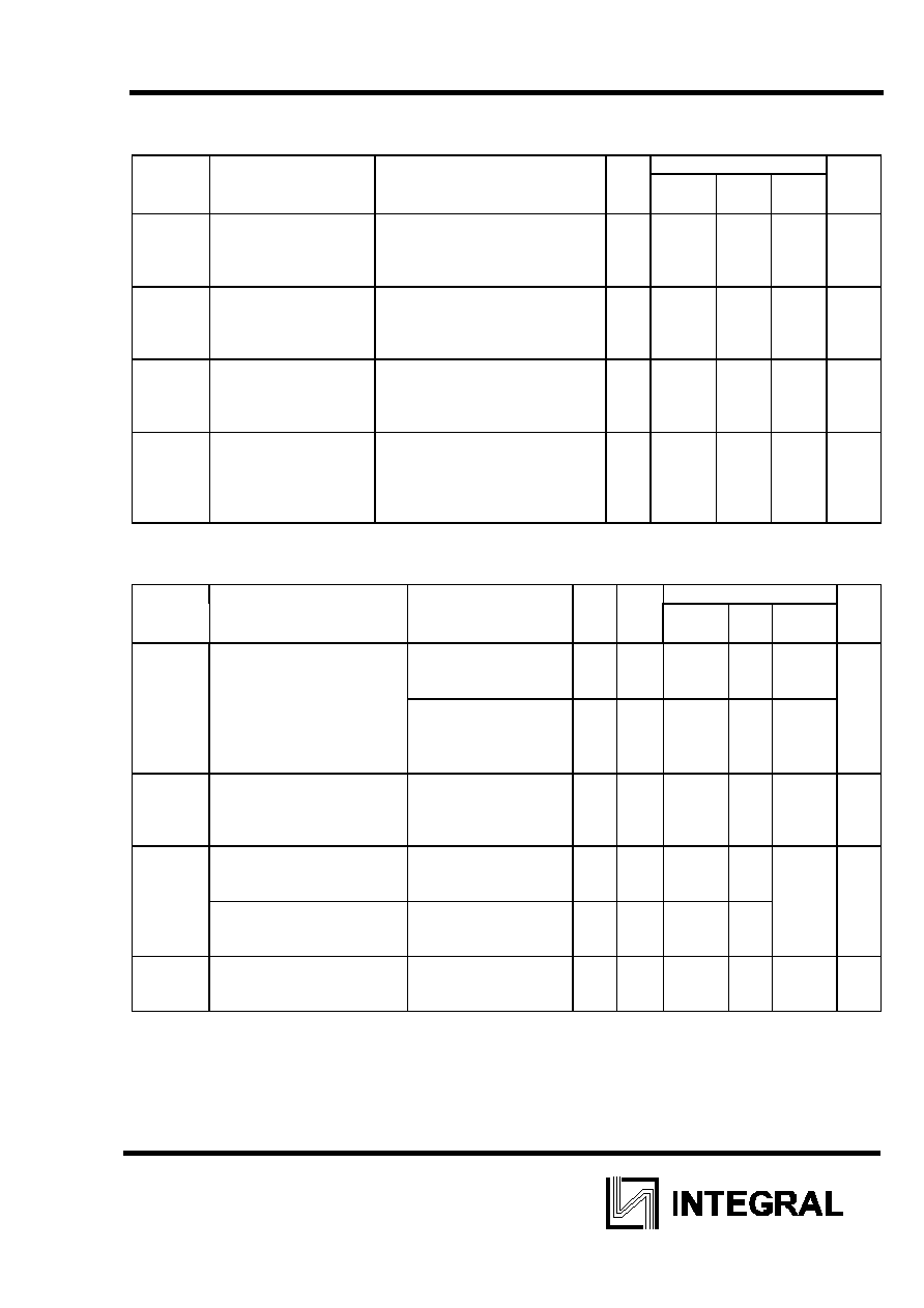
IN74HC4051
3
DC ELECTRICAL CHARACTERISTICS Digital Section (Voltages Referenced to GND) V
EE
=GND,
Except Where Noted
V
CC
Guaranteed
Limit
Symbol Parameter
Test
Conditions
V 25
�C to
-55
�C
�85
�C
�125
�C
Unit
V
IH
Minimum
High-Level
Input Voltage,
Channel-Select or
Enable Inputs
R
ON
= Per Spec
2.0
4.5
6.0
1.5
3.15
4.2
1.5
3.15
4.2
1.5
3.15
4.2
V
V
IL
Maximum Low -Level
Input Voltage,
Channel-Select or
Enable Inputs
R
ON
= Per Spec
2.0
4.5
6.0
0.3
0.9
1.2
0.3
0.9
1.2
0.3
0.9
1.2
V
I
IN
Maximum
Input
Leakage Current,
Channel-Select or
Enable Inputs
V
IN
=V
CC
or GND,
V
EE
=-6.0 V
6.0
0.1
1.0
1.0
A
I
CC
Maximum
Quiescent
Supply Current (per
Package)
Channel Select = V
CC
or GND
Enable = V
CC
or GND
V
IS
= V
CC
or GND
V
IO
= 0 V V
EE
= GND
V
EE
= - 6.0
6.0
6.0
2
8
20
80
40
160
A
DC ELECTRICAL CHARACTERISTICS Analog Section
V
CC
V
EE
Guaranteed
Limit
Symbol Parameter
Test
Conditions
V V 25
�C to
-55
�C
�85
�C
�125
�C
Unit
R
ON
Maximum
"ON"
Resistance
V
IN
=V
IL
or V
IH
V
IS
= V
CC
or V
EE
I
S
� 2.0 mA(Figure 1)
4.5
4.5
6.0
0.0
-4.5
-6.0
190
120
100
240
150
125
280
170
140
V
IN
=V
IL
or V
IH
V
IS
= V
CC
or V
EE
(Endpoints)
I
S
� 2.0 mA(Figure 1)
4.5
4.5
6.0
0.0
-4.5
-6.0
150
100
80
190
125
100
230
140
115
R
ON
Maximum Difference in
"ON" Resistance Between
Any Two Channels in the
Same Package
V
IN
=V
IL
or V
IH
V
IS
= 1/2 (V
CC
- V
EE
)
I
S
� 2.0 mA
4.5
4.5
6.0
0.0
-4.5
-6.0
30
12
10
35
15
12
40
18
14
I
OFF
Maximum Off- Channel
Leakage Current, Any
One Channel
V
IN
=V
IL
or V
IH
V
IO
= V
CC
- V
EE
Switch Off (Figure 2)
6.0 -6.0 0.1 0.5 1.0
A
Maximum Off- Channel
Leakage Current,
Common Channel
V
IN
=V
IL
or V
IH
V
IO
= V
CC
- V
EE
Switch Off (Figure 3)
6.0 -6.0 0.2 2.0 4.0
I
ON
Maximum On- Channel
Leakage Current,
Channel to Channel
V
IN
=V
IL
or V
IH
Switch to Switch =
V
CC
- V
EE
(Figure 4)
6.0 -6.0 0.2 2.0 4.0
A
IN74HC4051
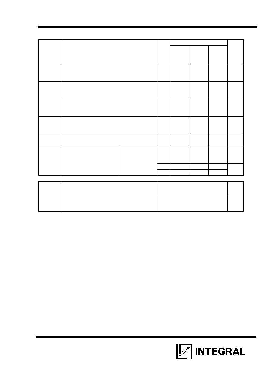
4
AC ELECTRICAL CHARACTERISTICS(C
L
=50pF,Input t
r
=t
f
=6.0 ns)
V
CC
Guaranteed Limit
Symbol Parameter V
25
�C
to
-55
�C
�85�C �125
�C
Unit
t
PLH
,
t
PHL
Maximum Propagation Delay, Channel-
Select to Analog Output (Figures 8 and
9)
2.0
4.5
6.0
370
74
63
465
93
79
550
110
94
ns
t
PLH
,
t
PHL
Maximum Propagation Delay , Analog
Input to Analog Output (Figures 10 and
11)
2.0
4.5
6.0
60
12
10
75
15
13
90
18
15
ns
t
PLZ
,
t
PHZ
Maximum Propagation Delay , Enable to
Analog Output (Figures 12 and 13)
2.0
4.5
6.0
290
58
49
364
73
62
430
86
73
ns
t
PZL
,
t
PZH
Maximum Propagation Delay , Enable to
Analog Output (Figures 12 and 13)
2.0
4.5
6.0
345
69
59
435
87
74
515
103
87
ns
C
IN
Maximum Input Capacitance, Channel-
Select or Enable Inputs
- 10 10 10 pF
C
I/O
Maximum
Capacitance
Analog
I/O
All Switches
Off
- 35 35 35 pF
Common
O/I -
130
130
130
Feedthrough
- 1.0 1.0 1.0
Power Dissipation Capacitance (Per
Package) (Figure 14)
Typical @25
�C,V
CC
=5.0 V,
V
EE
=0 V
C
PD
Used to determine the no-load dynamic
power consumption:
P
D
=C
PD
V
CC
2
f+I
CC
V
CC
45 pF
IN74HC4051
5
ADDITIONAL APPLICATION CHARACTERISTICS (GND = 0.0 V)
V
CC
V
EE
Limit
*
Symbol Parameter
Test
Conditions
V
V
25
�C Unit
BW Maximum
On-
Channel
Bandwidth or
Minimum
Frequency
Response
(Figure 5)
f
in
=1 MHz Sine Wave
Adjust f
in
Voltage to Obtain 0 dBm at
V
OS
Increase f
in
Frequence Until dB
Meter
Reads -3 dB
R
L
=50
, C
L
=10 pF
2.25
4.50
6.00
-2.25
-4.50
-6.00
80
80
80
MHz
- Off-Channel
Feedthrough
Isolation
(Figure 6)
f
in
= Sine Wave
Adjust f
in
Voltage to Obtain 0 dBm at
V
IS
f
in
= 10 kHz, R
L
=600
, C
L
=50 pF
2.25
4.50
6.00
-2.25
-4.50
-6.00
-50
-50
-50
dB
f
in
= 1.0 MHz, R
L
=50
, C
L
=10 pF
2.25
4.50
6.00
-2.25
-4.50
-6.00
-40
-40
-40
- Feedthrough
Noise,
Channel
Select Input to
Common O/I
(Figure 7)
V
IN
� 1 Mhz Square Wave (t
r
= t
f
= 6
ns)
Adjust R
L
at Setup so that I
S
= 0 A
Enable = GND
R
L
=600
, C
L
=50 pF
2.25
4.50
6.00
-2.25
-4.50
-6.00
25
105
135
mV
P
P
R
L
=10
, C
L
=10 pF
2.25
4.50
6.00
-2.25
-4.50
-6.00
35
145
190
THD Total
Harmonic
Distortion
(Figure 15)
f
in
= 1 kHz, R
L
=10 k
, C
L
=50 pF
THD = THD
Measured
- THD
Source
V
IS
=4.0 V
PP
sine wave
V
IS
=8.0 V
PP
sine wave
V
IS
=11.0 V
PP
sine wave
2.25
4.50
6.00
-2.25
-4.50
-6.00
0.10
0.08
0.05
%
* Limits not tested. Determined by design and verified by qualification.
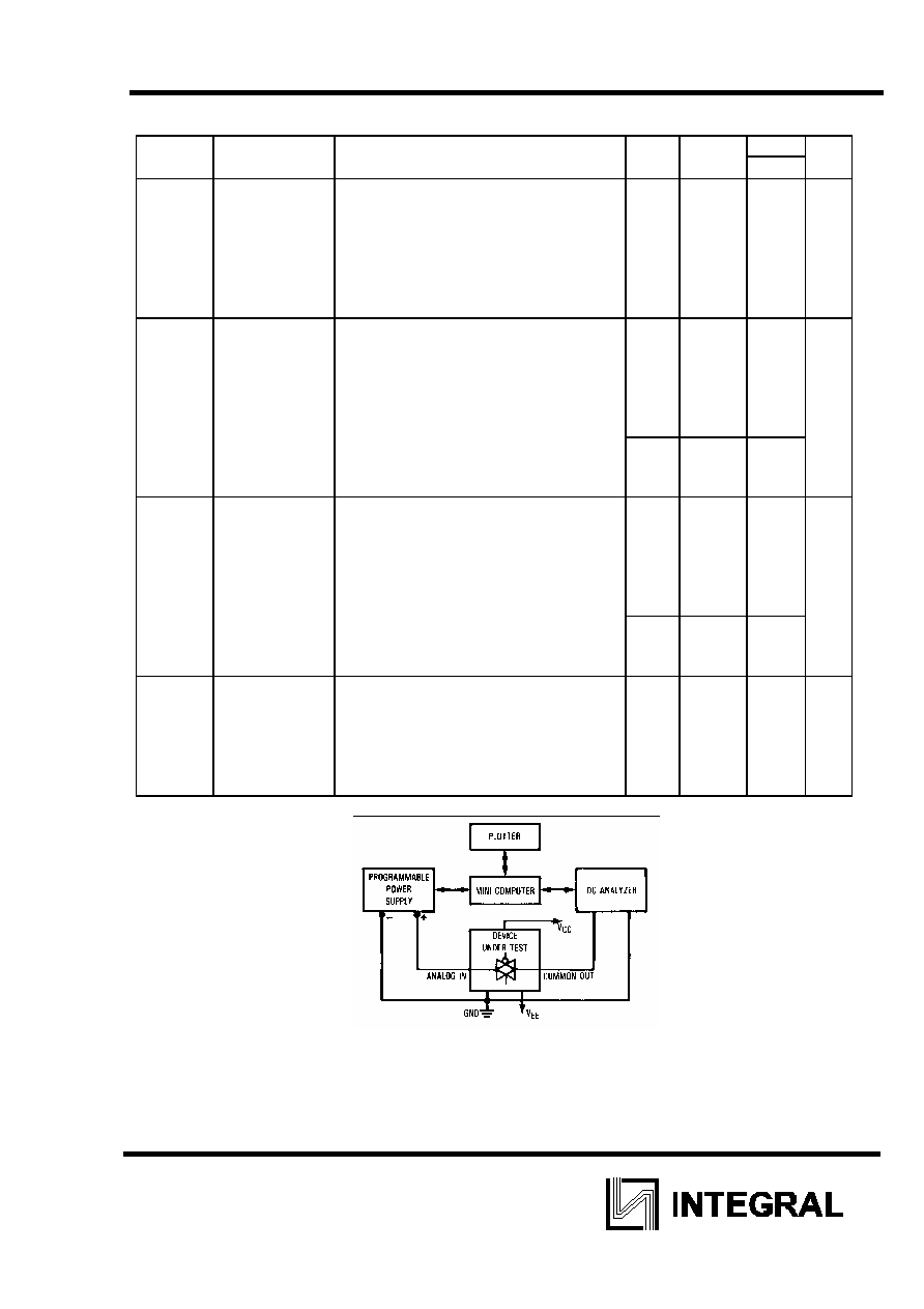
Figure 1. On Resistance Test Set-Up