
IN74HCT241A
1
O
CTAL
3-S
TATE
N
ONINVERTING
B
UFFER
/L
INE
D
RIVER
/L
INE
R
ECEIVER
High-Performance Silicon-Gate CMOS
The IN74HCT241A is identical in pinout to the LS/ALS241.
The IN74HCT241 may be used as a level converter for
interfacing TTL or NMOS outputs to High Speed CMOS inputs.
This octal noninverting buffer/line driver/line receiver is
designed to be used with 3-state memory address drivers, clock
drivers, and other bus-oriented systems. The device has
noninverting outputs and two output enables. Enable A is active-
low and Enable B is active-high.
û TTL/NMOS Compatible Input Levels
û Outputs Directly Interface to CMOS, NMOS, and TTL
û Operating Voltage Range: 4.5 to 5.5 V
û Low Input Current: 1.0 A
ORDERING INFORMATION
IN74HCT241AN Plastic
IN74HCT241ADW SOIC
T
A
= -55
ú to 125ú C for all
packages
FUNCTION TABLE
Inputs Output Inputs Outpu
t
Enable
A
A YA Enable
B
B YB
L L L H L L
L H H H H H
H X Z L X Z
X = don't care
Z = high impedance
LOGIC DIAGRAM
PIN 20=V
CC
PIN 10 = GND
PIN ASSIGNMENT
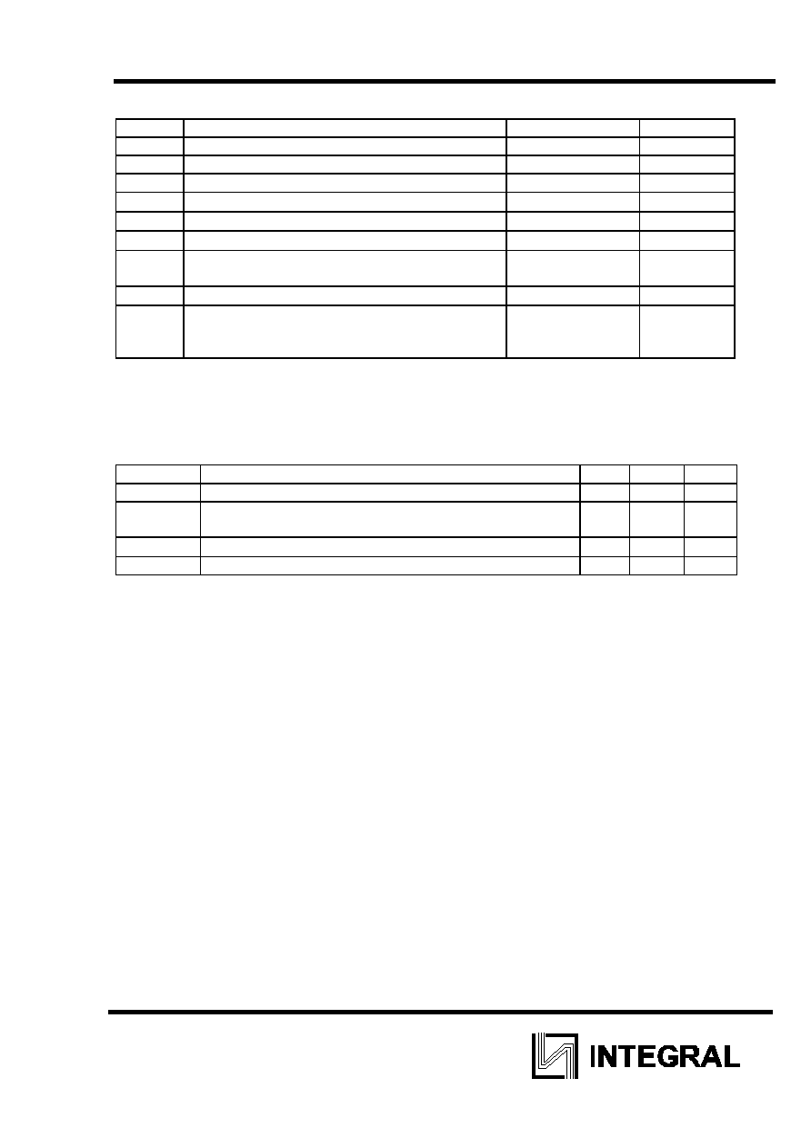
IN74HCT241A
2
MAXIMUM RATINGS
*
Symbol Parameter
Value
Unit
V
CC
DC Supply Voltage (Referenced to GND)
-0.5 to +7.0
V
V
IN
DC Input Voltage (Referenced to GND)
-1.5 to V
CC
+1.5
V
V
OUT
DC Output Voltage (Referenced to GND)
-0.5 to V
CC
+0.5
V
I
IN
DC Input Current, per Pin
20
mA
I
OUT
DC Output Current, per Pin
35
mA
I
CC
DC Supply Current, V
CC
and GND Pins
75
mA
P
D
Power Dissipation in Still Air, Plastic DIP+
SOIC Package+
750
500
mW
Tstg
Storage Temperature
-65 to +150
úC
T
L
Lead Temperature, 1 mm from Case for 10
Seconds
(Plastic DIP or SOIC Package)
260
úC
*
Maximum Ratings are those values beyond which damage to the device may occur.
Functional operation should be restricted to the Recommended Operating Conditions.
+Derating - Plastic DIP: - 10 mW/
úC from 65ú to 125úC
SOIC Package: : - 7 mW/
úC from 65ú to 125úC
RECOMMENDED OPERATING CONDITIONS
Symbol Parameter Min
Max
Unit
V
CC
DC Supply Voltage (Referenced to GND)
4.5
5.5
V
V
IN
, V
OUT
DC Input Voltage, Output Voltage (Referenced to
GND)
0 V
CC
V
T
A
Operating Temperature, All Package Types
-55
+125
úC
t
r
, t
f
Input Rise and Fall Time (Figure 1)
0
500
ns
This device contains protection circuitry to guard against damage due to high static
voltages or electric fields. However, precautions must be taken to avoid applications of any voltage
higher than maximum rated voltages to this high-impedance circuit. For proper operation, V
IN
and
V
OUT
should be constrained to the range GND
ò(V
IN
or V
OUT
)
òV
CC
.
Unused inputs must always be tied to an appropriate logic voltage level (e.g., either GND or
V
CC
). Unused outputs must be left open.
IN74HCT241A
3
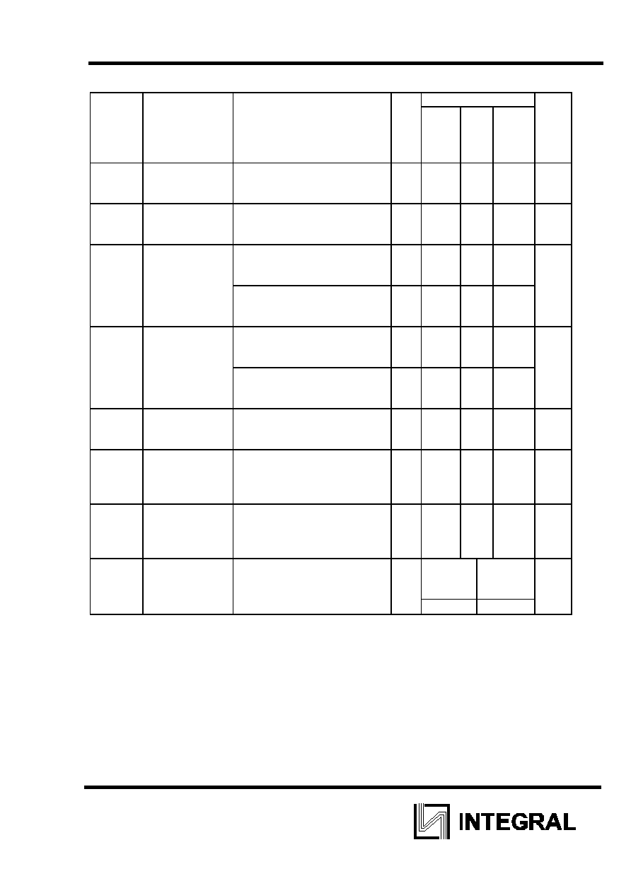
DC ELECTRICAL CHARACTERISTICS(Voltages Referenced to GND)
V
CC
Guaranteed Limit
Symbol Parameter
Test
Conditions
V 25
úC to
-
55
úC
ò85
úC
ò125
úC
Unit
V
IH
Minimum
High-
Level Input
Voltage
V
OUT
= V
CC
-0.1 V
I
OUT
ò 20 A
4.5
5.5
2.0
2.0
2.0
2.0
2.0
2.0
V
V
IL
Maximum
Low
-Level Input
Voltage
V
OUT
= 0.1 V
I
OUT
ò 20 A
4.5
5.5
0.8
0.8
0.8
0.8
0.8
0.8
V
V
OH
Minimum
High-
Level Output
Voltage
V
IN
= V
IH
I
OUT
ò 20 A
4.5
5.5
4.4
5.4
4.4
5.4
4.4
5.4
V
V
IN
= V
IH
I
OUT
ò 6.0 mA
4.5
3.98
3.8
4
3.7
V
OL
Maximum
Low-Level
Output Voltage
V
IN
= V
IL
I
OUT
ò 20 A
4.5
5.5
0.1
0.1
0.1
0.1
0.1
0.1
V
V
IN
= V
IL
I
OUT
ò 6.0 mA
4.5
0.26
0.3
3
0.4
I
IN
Maximum
Input Leakage
Current
V
IN
=V
CC
or GND
5.5
0.1 1.
0
1.0
A
I
OZ
Maximum
three State
Leakage
Current
Output in High-Impedance
State
V
IN
= V
IL
or V
IH
V
OUT
=V
CC
or GND
5.5
0.5 5.
0
10.0
A
I
CC
Maximum
Quiescent
Supply Current
(per Package)
V
IN
=V
CC
or GND
I
OUT
=0
A
5.5 4.0 40 160
A
I
CC
Additional
Quiescent
V
IN
= 2.4 V, Any One Input
V
IN
=V
CC
or GND, Other
Inputs
ô-55úC 25úC to
125
úC
mA
Supply
Current
I
OUT
=0
A
5.5 2.9
2.4
NOTE: Total Supply Current = I
CC
+
I
CC

IN74HCT241A
4
AC ELECTRICAL CHARACTERISTICS(V
CC
=5.0 V
10%, C
L
=50pF,Input t
r
=t
f
=6.0 ns)
Guaranteed
Limit
Symbol Parameter 25
úC
to
-55
úC
ò85úC ò125
úC
Unit
t
PLH
,
t
PHL
Maximum Propagation Delay, A to YA or
B to YB (Figures 1 and 3)
23 29 35 ns
t
PLZ
,
t
PHZ
Maximum Propagation Delay, Output
Enable to YA or YB (Figures 2 and 4)
30 38 45 ns
t
PZH
,
t
PZL
Maximum Propagation Delay, Output
Enable to YA or YB (Figures 2 and 4)
26 33 39 ns
t
TLH
, t
THL
Maximum Output Transition Time, Any
Output
(Figures 1 and 3)
12 15 18 ns
C
IN
Maximum Input Capacitance
10
10
10
pF
C
OUT
Maximum
Three-State
Output
Capacitance
(Output in High-Impedance State)
15 15 15 pF
Power Dissipation Capacitance (Per
Enable Output)
Typical @25
úC,V
CC
=5.0
V
C
PD
Used to determine the no-load dynamic
power consumption:
P
D
=C
PD
V
CC
2
f+I
CC
V
CC
55 pF
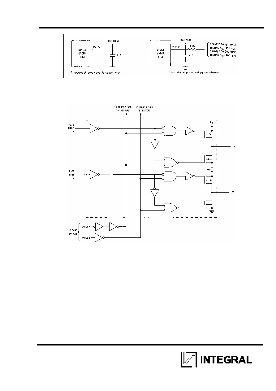
Figure 1. Switching Waveforms
Figure 2. Switching Waveforms
IN74HCT241A
5
Figure 3. Test Circuit
Figure 4. Test Circuit
EXPANDED LOGIC DIAGRAM
(1/4 of the Device)