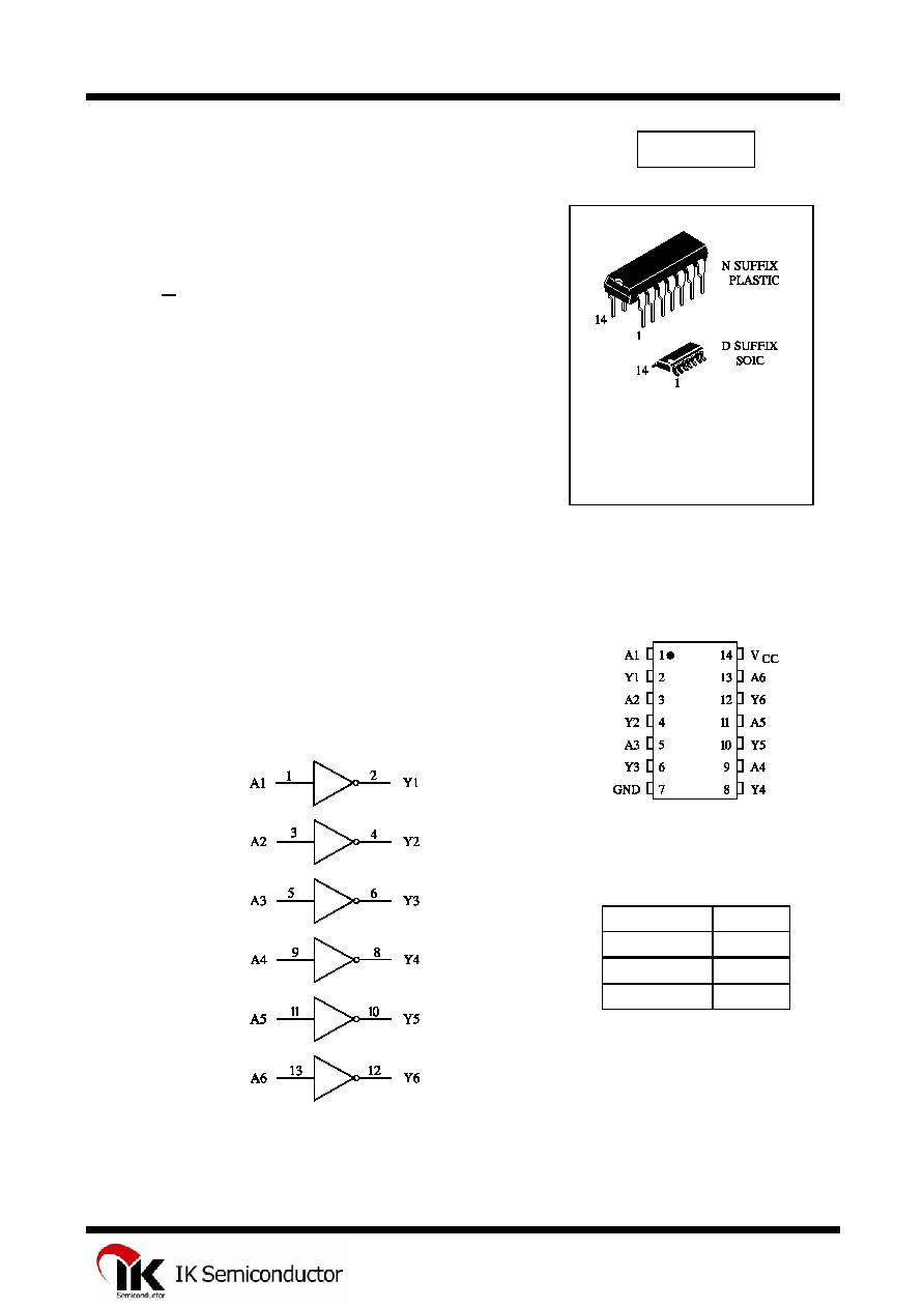
IN74LS04
MAXIMUM RATINGS
*
Symbol Parameter
Value
Unit
V
CC
Supply Voltage
7.0
V
V
IN
Input Voltage
7.0
V
V
OUT
Output Voltage
7.0
V
Tstg
Storage Temperature Range
-65 to +150
úC
*
Maximum Ratings are those values beyond which damage to the device may occur.
Functional operation should be restricted to the Recommended Operating Conditions.
RECOMMENDED OPERATING CONDITIONS
Symbol Parameter
Min
Max
Unit
V
CC
Supply Voltage
4.75
5.25
V
I
OH
High Level Output Current
-400
V
I
OL
Low Level Output Current
8.0
V
T
A
Ambient Temperature Range
0
+70
úC
DC ELECTRICAL CHARACTERISTICS over full operating conditions
Guaranteed
Limit
Symbol Parameter
Test
Conditions
Min
Max
Unit
V
IH
High Level Input Voltage
2
V
V
IL
Low Level Input Voltage
0.8
V
V
IK
Input Clamp Voltage
V
CC
= min, I
I
= -18 mA
-1.5
V
V
OH
High Level Output Current
V
CC
= min, V
IL
=max
I
OH
= max
2.7
V
V
OL
Low Level Output Voltage
V
CC
= min, V
IH
=min,
I
OL
= 8 mA
0.5
V
I
I
Input Current at maximum input
voltage
V
CC
= max, V
I
= -7V
0.1
mA
I
IH
High Level Input Current
V
CC
= max, V
IN
= 2.7 V
20
A
I
IL
Low Level Input Current
V
CC
= max, V
IN
= 0.4 V
-0.4
mA
I
OS
Short-circuit output current
V
CC
= max (Note)
-20
-100
mA
I
CC
Supply Current
V
CC
= max
Total with
outputs high
2.4
mA
Total
with
outputs low
6.6
Note: Not more than one output should be shorted at a time, and duration should not exceed one second.
2
IN74LS04
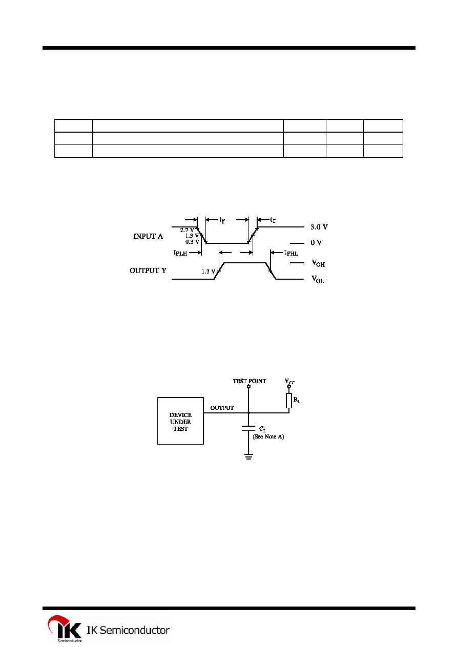
AC ELECTRICAL CHARACTERISTICS
(V
CC
= 5.0 V, C
L
= 15 pF, T
A
=25
úC, R
L
= 2 k
,
t
r
=15 ns, t
f
= 6.0 ns)
Symbol Parameter Min
Max
Unit
t
PLH
Propagation Delay Time
15
ns
t
PHL
Propagation Delay Time
15
ns
Figure 1. Switching Waveforms
NOTE A. C
L
includes probe and jig capacitance.
Figure 2. Test Circuit
3
IN74LS04
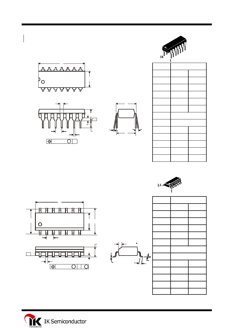
N SUFFIX PLASTIC DIP
(MS - 001AA)
Symbol
MIN
MAX
A
18.67
19.69
B
6.1
7.11
C
5.33
D
0.36
0.56
F
1.14
1.78
G
H
J
0
ú
10
ú
K
2.92
3.81
NOTES:
L
7.62
8.26
1.
Dimensions "A", "B" do not include mold flash or protrusions.
M
0.2
0.36
Maximum mold flash or protrusions 0.25 mm (0.010) per side.
N
0.38
D SUFFIX SOIC
(MS - 012AB)
Symbol
MIN
MAX
A
8.55
8.75
B
3.8
4
C
1.35
1.75
D
0.33
0.51
F
0.4
1.27
G
H
J
0ú
8ú
NOTES:
K
0.1
0.25
1.
Dimensions A and B do not include mold flash or protrusion.
M
0.19
0.25
2.
Maximum mold flash or protrusion 0.15 mm (0.006) per side
P
5.8
6.2
for A; for B 0.25 mm (0.010) per side.
R
0.25
0.5
Dimension, mm
1.27
5.27
2.54
7.62
Dimension, mm
A
B
H
C
K
C M
J
F
M
P
G
D
R x 45
SEATING
PLANE
0.25 (0.010) M T
-T-
1
14
7
8
A
B
F
G
D
L
H
SEATING
PLANE
N
K
0.25 (0.010) M T
M
J
-T-
C
1
14
7
8
4