
TECHNICAL DATA
OCTAL BUFFER / DRIVER
WITH 3-STATE OUTPUTS
This octal buffer/driver is designed specially to
improve both the performance and density of 3-state
memory address drivers, clock drivers and bus-
oriented receivers and transmitters. When this device is
used with the `ALS241, `AS241A, `ALS244 and
AS244A, the circuit designer has a choice of selected
combinations of inverting and noninverting outputs,
symmetrical active-low output-enable (OE) inputs and
complementary OE and OE inputs. This device features
high fan-out and improved fan-in.
The IN74ALS240A is characterized for operation from
0
o
C to 70
o
C.
ORDERING INFORMATION
IN74LS240AN Plastic
IN74ALS240AD SOIC
T
A
= 0
ú
to 70
ú
C for all
packages
Logic Symbol
Logic Diagram (Positive Logic)
IN74ALS240A
IN74ALS240A
2
ABSOLUTE MAXIMUM RATINGS
OVER OPERATING FREE-AIR TEMPERATURE RANGE
Supply voltage, Vcc
7 V
Input voltage, V
I
7 V
Voltage applied to a disabled 3-state output
5.5V
Operating free-air temperature range, T
A
0
o
C to 70
o
C.
Storage temperature range
-65
o
C to 150
o
C
RECOMMENDED OPERATING CONDITIONS
MIN
NOM MAX UNIT
V
CC
Supply voltage
4.5
5
5.5
V
V
IH
High-level input voltage
2
V
V
IL
Low-level input voltage
0.8
V
I
OH
High-level output current
-15
mA
I
OL
Low-level output current
24
mA
T
A
Operating free-air temperature
0
70
o
C
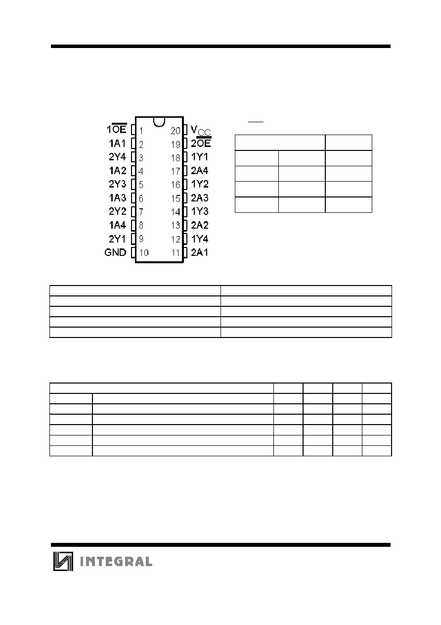
FUNCTION TABLE
INPUTS
OUTPUT
OE
A
Y
L
H
L
L
L
H
H
X
Z
PIN ASSIGNMENT
IN74ALS240A
3
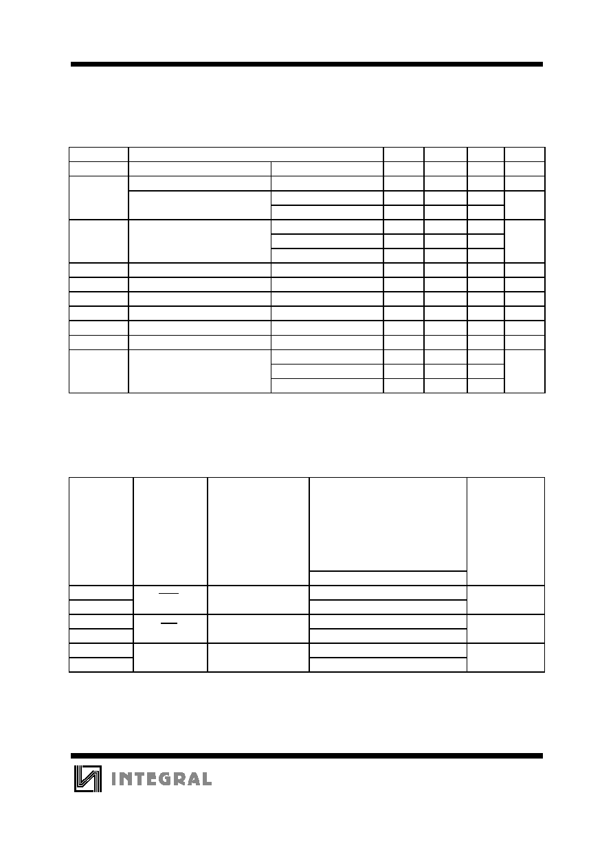
ELECTRICAL CHARACTERISTICS OVER RECOMMENDED OPERATING FREE-
AIR TEMPERATURE RANGE
Parameter
Test Conditions
MIN
TYP** MAX UNIT
V
IK
V
CC
= 4.5V
I
I
= -18mA
-1.2
V
V
CC
= 4.5V to 5.5V
I
OH
= -0.4mA
V
CC
-2
V
V
OH
V
CC
= 4.5V
I
OH
= -3mA
2.4
3.2
V
I
OH
= -15mA
2
V
OL
V
CC
= 4.5V
I
OL
= 12 mA
0.25
0.4
I
OL
= 24 mA
0.35
0.5
V
I
OL
= 48 mA*
0.35
0.5
I
OZH
V
CC
= 5.5V
V
O
= 2.7V
20
A
I
OZL
V
CC
= 5.5V
V
O
= 0.4V
-20
A
I
I
V
CC
= 5.5V
V
I
= 7V
0.1
mA
I
IH
V
CC
= 5.5V
V
I
= 2.7V
20
A
I
IL
V
CC
= 5.5V
V
I
= 0.4V
-0.1
m
I
O
***
V
CC
= 5.5V
V
O
= 2.25V
-30
-112
m
Output high
4
11
I
CC
V
CC
= 5.5V
Outputs low
13
23
m
Outputs disabled
14
25
*- Applies only to the -1 version and only if V
CC
is between 4.75V and 5.25V
**- All typical values are at V
CC
=5V, T
A
=25
o
C
***- The output conditions have been chosen to produce a current that closely approximates one half of the true
short-circuit output current, I
OS
SWITCHING CHARACTERISTICS
Parameter From (input)
To (output)
V
CC
= 4.5 V to 5.5 V
C
L
= 50 pF
R
1
= 500
R
2
= 500
T
A
= MIN to MAX*
UNIT
MIN MAX
t
PLH
A
Y
2 9
ns
t
PHL
2 9
t
PZH
OE
Y
5 13
ns
t
PZL
5 18
t
PHZ
OE
Y
2 10
ns
t
PLZ
3 12
*- For conditions shown as MIN and MAX, use the appropriate value specified under recommended operating
conditions