
TECHNICAL DATA
1
INTEGRAL
OCTAL BUFFER/LINE DRIVE; 3-STATE
The IN74LV241 is a low-voltage Si-gate CMOS device and is pin and
function compatible with IN74HC/HCT241.
The IN74LV241 is an octal non-inverting buffer/line driver with 3-
state outputs. The 3-state outputs are controlled by the output enable
inputs 1OE and 2OE.
û
Outputs Directly Interface to CMOS, NMOS, and TTL
û
Operating Voltage Range: 1.2 to 3.6 V
û
Low Input Current: 1.0
A, 0.1
at = 25
ú
û
Output Current: 8 mA at V
CC
= 3.0 V
û
High Noise Immunity Characteristic of CMOS Devices
IN74LV241
N SUFFIX
PLASTIC DIP
DW SUFFIX
SO
1
20
1
20
ORDERING INFORMATION
IN74LV241N
Plastic DIP
IN74LV241DW
SOIC
IZ74LV241
chip
T
A
= -40
ú
to 125
ú
C for all packages
FUNCTION TABLE
Input
Output
Input
Output
1OE
1An
1Yn
2OE
2An
2Yn
L
L
L
H
L
L
L
H
H
H
H
H
H
X
Z
L
X
Z
H= high level
L = low level
X = don't care
Z = high impedance
LOGIC DIAGRAM
PIN 20=V
CC
PIN 10 = GND
PIN ASSIGNMENT
1
2
3
5
4
6
7
8
9
10
V
CC
20
18
17
16
15
14
19
11
12
13
GND
2OE
1OE
1A
0
2Y
3
1A
1
2Y
2
1A
2
2Y
1
1A
3
2Y
0
1Y
0
2A
3
1Y
1
2A
2
1Y
2
2A
1
1Y
3
2A
0
2
11
6
15
4
13
8
17
1
19
1A0
1Y0
2A0
2Y0
1A2
1Y2
2A0
2Y0
1A1
1Y1
2A1
2Y1
1A3
1Y3
2A1
2Y1
1OE
2OE
18
9
14
5
16
7
12
3
DATA
INPUTS
NONINVERTING
OUTPUTS
OUTPUT
ENABLES

IN74LV241
2
INTEGRAL
MAXIMUM RATINGS
*
Symbol
Parameter
Value
Unit
V
CC
DC supply voltage
-0.5 to +5.0
V
I
IK
*
1
DC Input diode current
20
mA
I
OK
*
2
DC Output diode current
50
mA
I
O
*
3
DC Output source or sink current
35
mA
I
CC
DC V
CC
current
70
mA
I
GND
DC GND current
70
mA
P
D
Power dissipation per package: *
4
Plastic DIP
SO
750
500
mW
Tstg
Storage Temperature
-65 to +150
ú
C
T
L
Lead Temperature, 1.5 mm (Plastic DIP Package), 0.3 mm (SO
Package) from Case for 4 Seconds
260
ú
C
*
Maximum Ratings are those values beyond which damage to the device may occur.
Functional operation should be restricted to the Recommended Operating Conditions.
*
1
V
I
< -0.5 V or V
I
> V
CC
+ 0.5 V.
*
2
V
O
< -0.5 V or V
O
> V
CC
+ 0.5 V.
*
3
-0.5 V < V
O
< V
CC
+ 0.5 V.
*
4
Derating - Plastic DIP: - 12 mW/
ú
C from 70
ú
to 125
ú
C
SO Package: : - 8 mW/
ú
C from 70
ú
to 125
ú
C
RECOMMENDED OPERATING CONDITIONS
Symbol
Parameter
Min
Max
Unit
V
CC
DC Supply Voltage
1.2
3.6
V
V
I
Input Voltage
0
V
CC
V
V
O
Output Voltage
0
V
CC
V
T
A
Operating Temperature, All Package Types
-40
+125
ú
C
t
r
, t
f
Input Rise and Fall Time (Figure 1)
V
CC
=1.2 V
V
CC
=2.0 V
V
CC
=3.0 V
V
CC
=3.6 V
0
0
0
0
1000
700
500
400
ns
This device contains protection circuitry to guard against damage due to high static voltages or electric
fields. However, precautions must be taken to avoid applications of any voltage higher than maximum rated voltages
to this high-impedance circuit. For proper operation, V
IN
and V
OUT
should be constrained to the range GND
ò
(V
IN
or
V
OUT
)
ò
V
CC
.
Unused inputs must always be tied to an appropriate logic voltage level (e.g., either GND or V
CC
). Unused
outputs must be left open.

IN74LV241
3
INTEGRAL
DC ELECTRICAL CHARACTERISTICS
(Voltages Referenced to GND)
Test
V
CC
Guaranteed Limit
Symbol
Parameter
conditions
V
25
ú
C
-40
ú
C to 85
ú
C
125
ú
C
Unit
min
max
min
max
min
max
V
IH
HIGH level input
voltage
1.2
2.0
3.0
3.6
0.9
1.4
2.1
2.5
-
-
-
-
0.9
1.4
2.1
2.5
-
-
-
-
0.9
1.4
2.1
2.5
-
-
-
-
V
V
IL
LOW level input
voltage
1.2
2.0
3.0
3.6
-
-
-
-
0.3
0.6
0.9
1.1
-
-
-
-
0.3
0.6
0.9
1.1
-
-
-
-
0.3
0.6
0.9
1.1
V
V
OH
HIGH level output
voltage
V
I
= V
IH
or V
IL
I
O
= -50
1.2
2.0
3.0
3.6
1.1
1.92
2.92
3.52
-
-
-
-
1.0
1.9
2.9
3.5
-
-
-
-
1.0
1.9
2.9
3.5
-
-
-
-
V
V
I
= V
IH
or V
IL
I
O
= -8 m
3.0
2.48
-
2.34
-
2.20
-
V
V
OL
LOW level output
voltage
V
I
= V
IH
or V
IL
I
O
= 50
1.2
2.0
3.0
3.6
-
-
-
-
0.09
0.09
0.09
0.09
-
-
-
-
0.1
0.1
0.1
0.1
-
-
-
-
0.1
0.1
0.1
0.1
V
V
I
= V
IH
or V
IL
I
O
= 8 m
3.0
-
0.33
-
0.4
-
0.5
V
I
I
Input current
V
I
= V
CC
or 0 V
*
-
0.1
-
1.0
-
1.0
I
OZ
Three state leakage
current
3-state outputs
V
I
(01,19) = V
IH
V
O
=V
CC
or 0 V
1.2
*
-
0.5
-
5
-
10
I
CC
Supply current
V
I
=V
CC
or 0 V
I
O
= 0
*
-
8.0
-
80
-
160
* V
CC
= 3.3
0.3 V
IN74LV241
4
INTEGRAL
AC ELECTRICAL CHARACTERISTICS
(C
L
=50 pF, t
r
=t
f
=6.0 ns)
Test
V
CC
Guaranteed Limit
Symbol
Parameter
conditions
V
25
ú
C
-40
ú
C to
85
ú
C
125
ú
C
Unit
min max
min
max
min
max
t
PHL,
t
PLH
Propagation delay , 1An
to 1Yn, 2An to 2Yn
V
I
= 0 V or V
CC
Figure 1 and 3
1.2
2.0
*
-
-
-
100
24
15
-
-
-
125
30
19
-
-
-
150
36
23
ns
t
PHZ
t
PLZ
Propagation delay, 1OE to
1Yn, 2OE to 2Yn
V
I
= 0 V or V
CC
Figure 2 and 4
1.2
2.0
*
-
-
-
140
30
20
-
-
-
175
35
24
-
-
-
210
41
28
ns
t
PZH
t
PZL
Propagation delay, 1OE to
1Yn, 2OE to 2Yn
V
I
= 0 V or V
CC
Figure 2 and 4
1.2
2.0
*
-
-
-
140
32
20
-
-
-
175
40
25
-
-
-
210
48
30
ns
t
THL,
t
TLH
Output Transition Time,
Any Output
V
I
= 0 V or V
CC
Figure 1 and 3
1.2
2.0
*
-
-
-
60
16
10
-
-
-
75
20
13
-
-
-
90
24
15
ns
C
I
Input capacitance
3.0
-
7.0
-
7.0
-
7.0
pF
C
PD
Power dissipation
capacitance (per one
channel)
V
I
= 0 V or V
CC
-
70
-
-
-
-
pF
* V
CC
= 3.3
0.3 V
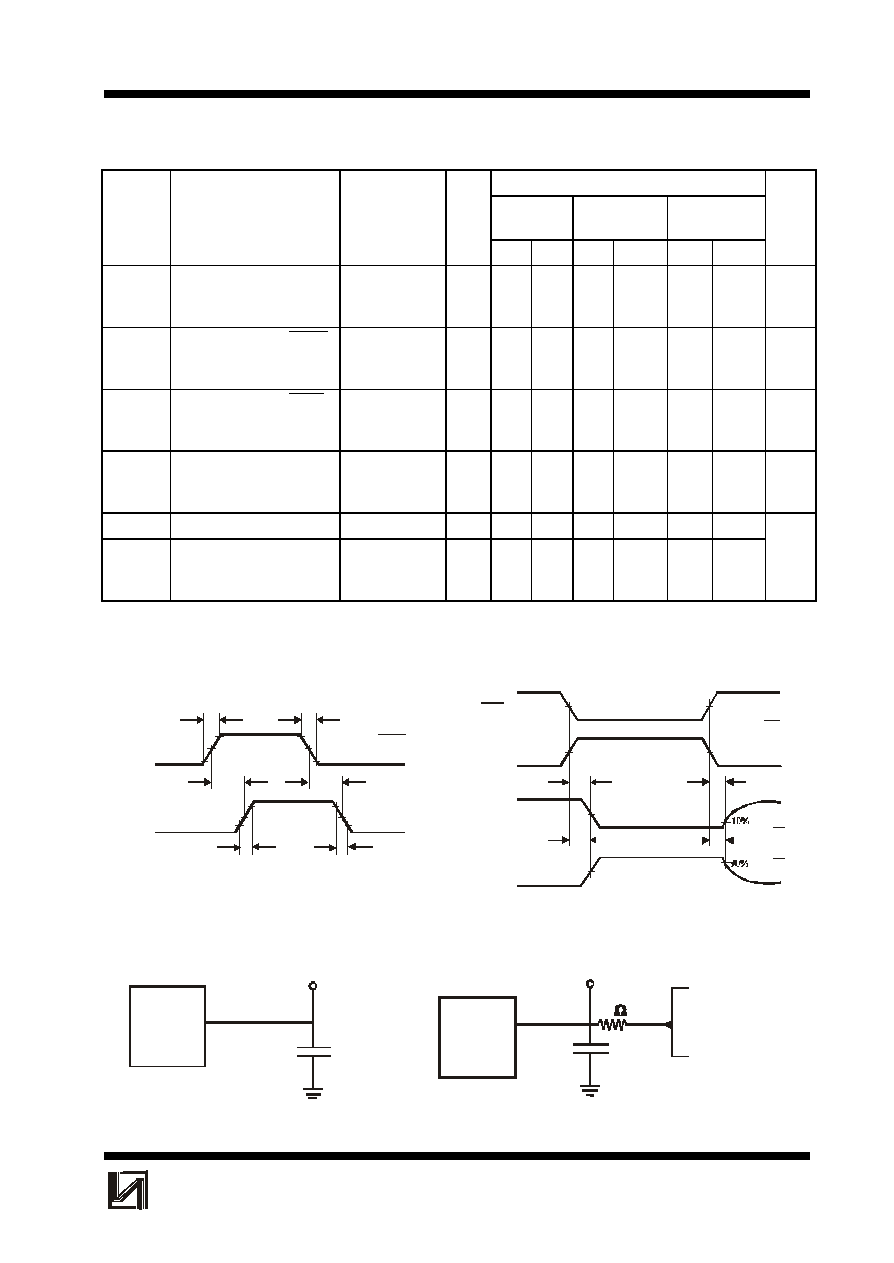
Figure 1. Switching Waveforms
Figure 2. Switching Waveforms
* Includes all probe and jig capacitance
* Includes all probe and jig capacitance
90%
90%
50%
50%
10%
10%
t
t
t
t
t
t
f
r
PLH
TLH
THL
PHL
V
CC
GND
1A or 2A
n
n
1Y or 2Y
n
n
DEVICE
UNDER
TEST
OUTPUT
C
L
*
TEST POINT
DEVICE
UNDER
TEST
OUTPUT
1 k
C
L
*
TEST POINT
Connect to V
CC
when
testing t
PLZ
and t
PZL
Connect to GND
when
testing t
PHZ
and t
PZH
t
t
t
t
PZH
PHZ
PZL
PLZ
V
V
V
CC
CC
OH
GND
GND
50%
50%
50%
50%
)
2OE
1OE
1Y or 2Y
n
n
1Y or 2Y
n
n
GND
V
V
CC
OL
IN74LV241
5
INTEGRAL
Figure 3. Test Circuit
Figure 4. Test Circuit
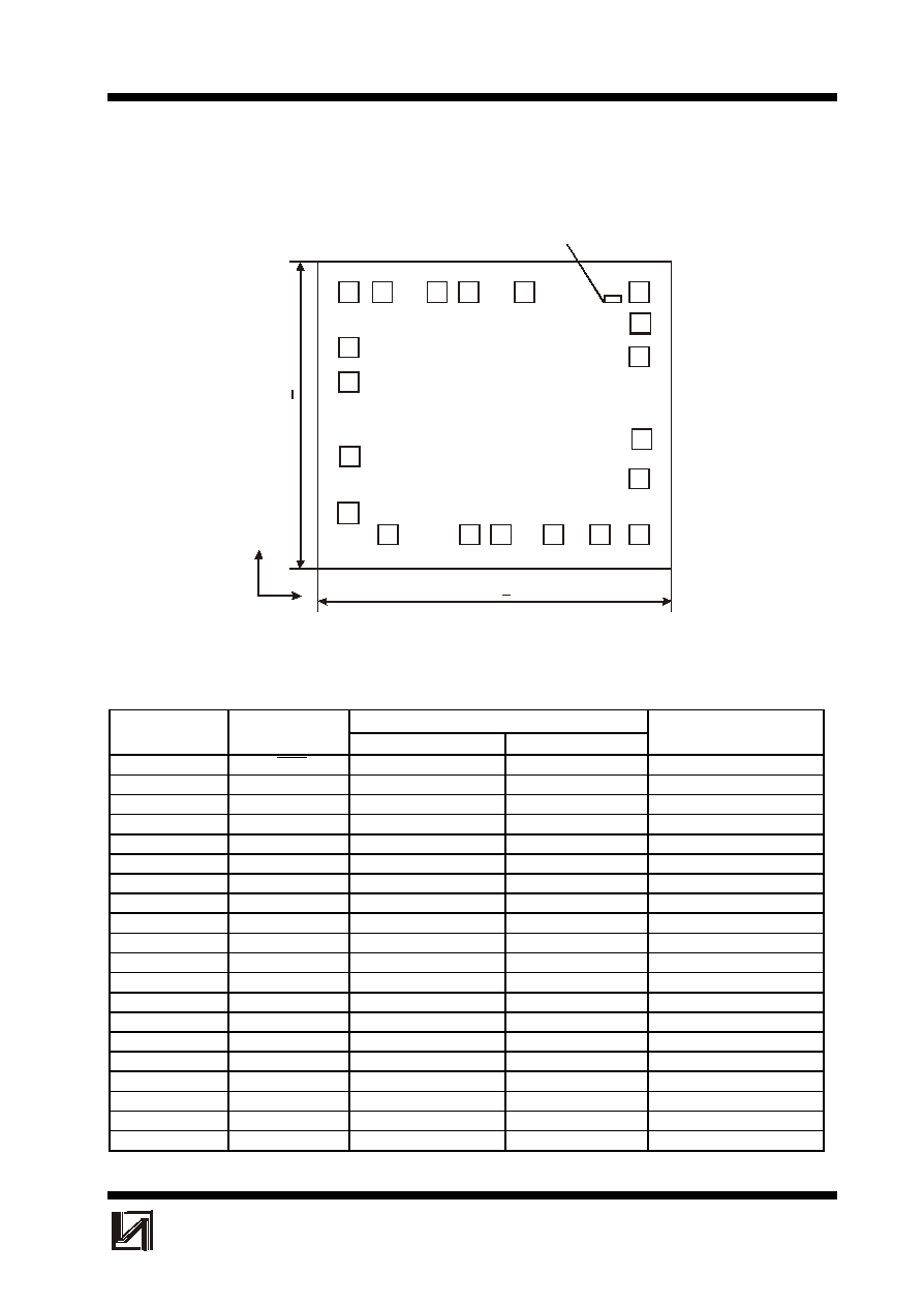
CHIP PAD DIAGRAM
Location of marking (mm): left lower corner x=1.539, y=1.433.
Chip thickness: 0.46
0.02 mm.
PAD LOCATION
Location (left lower corner), mm
Pad No
Symbol
X
Y
Pad size, mm
01
1OE
0.115
0.55
0.108 x 0.108
02
1A
0
0.1075
0.246
0.108 x 0.108
03
2Y
3
0.3215
0.131
0.108 x 0.108
04
1A
1
0.76
0.131
0.108 x 0.108
05
2Y
2
0.9285
0.131
0.108 x 0.108
06
2A
2
1.2115
0.131
0.108 x 0.108
07
2Y
1
1.4615
0.131
0.108 x 0.108
08
2A
3
1.674
0.131
0.108 x 0.108
09
2Y
0
1.674
0.43
0.108 x 0.108
10
GND
1.685
0.643
0.108 x 0.108
11
2A
0
1.674
1.0855
0.108 x 0.108
12
1Y
3
1.6795
1.266
0.108 x 0.108
13
2A
1
1.674
1.4345
0.108 x 0.108
14
1Y
2
1.0525
1.4345
0.108 x 0.108
15
2A
2
0.7545
1.4345
0.108 x 0.108
16
1Y
1
0.586
1.4345
0.108 x 0.108
17
2A
3
0.293
1.4345
0.108 x 0.108
18
1Y
0
0.112
1.4345
0.108 x 0.108
19
2OE
0.112
1.1385
0.108 x 0.108
20
V
CC
0.112
0.949
0.108 x 0.108
Note: Pad location is given as per metallization layer
02
(0,0)
X
Y
Chip marking
25LV241
03
04 05
06
07
08
09
10
1.9 + 0.03
1
.
6
5
+
0
.
0
3
11
12
01
14
15
16
17
18
19
20
13