TECHNICAL DATA
IN74VHCT74
Dual D Flip-Flop with Set and Reset
IN74VHCT74 is high-speed logic IC made by CMOS
technology and designed for use in high-performance
calculating systems with a wide supply voltage range.
As for operation speed, IN74VHCT74 can be compared
with equivalent bipolar ICs based on Schottky TTL and two
times surpasses ICs of IN74Õ— series.
IN74VHCT74 tolerates operation under conditions when
voltage on input & output is exceeded up to 7V without
affecting characteristics and IC reliability. This possibility
allows to use IN74VHCT74 in radio-electronic devices for
interfacing with supply voltages 5V and 3V, eliminate IC
failure under supply voltage source emergency outage.
Use of output edge shaping block in the microcircuit
allows to reduce noise amplitude of noises when switching
outputs into the same state simultaneously.
Input levels of IN74VHCT74 are compatible with TTL level
and output levels with CMOS levels.
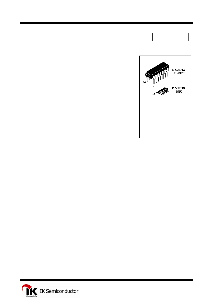
ORDERING INFORMATION
IN74VHCT74N Plastic
IN74VHCT74D SOIC
T
A
= -40
ú to 85ú C for all
packages
Features:
û
Supply voltage range 4.5 to 5.5 V.
û
Output current 8 mA.
û
Low consumption current: 0.2 mkA (typical value) at “ý = 25
ú—.
û
Latchup current not less than 300 mA at “ý = 85
ú—.
û
Tolerable value of static potential not less than 2000 V as per human body model (HBM) and
not less than 200 V as per machine model (ÃÃ).
û
Ambient operation temperature minus 40 to plus 85
ú—.
û
Balanced signal propagation delay.
û
Ensures voltage exceeding mode on input
û
Low noise level at the simultaneous switching of outputs in the same state:
V
OLP
= 0.8 V (max).
û
For pins and functions, compatible with IN74HCT74.
.
1
IN74VHCT74
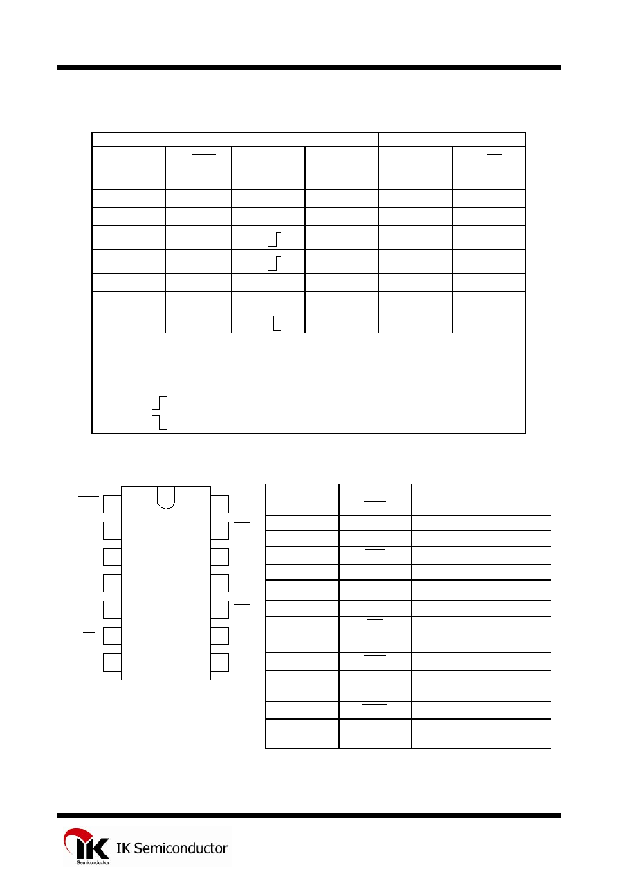
IN74VHCT74 truth table
Input Output
nSD
nRD
nCP nD nQ
nQ
L H X X H L
H L X X L H
L L X X H H
H H
H H L
H H
L L H
H H L X Qo Qo
H H H X Qo Qo
H H
X Qo Qo
Note - H - high voltage level;
L - low voltage level;
X - any voltage level (low or high);
Qo - storage of the previous state;
Z - output in the third
- transition from low into high level;
- transition from high into low level
Pinout
Pins description in IN74VHCT74
Pin No.
Symbol
Description
01
1RD
Input of RESET signal
02
1D
Data input
03
1CP
Input of clock signal
04
1SD
Input of SET signal
05 1Q
Data
output
06
1Q
Data output
07 GND
Common output
08
2Q
Data output
09 2Q
Data
output
10
2SD
Input of SET signal
11
2CP
Input of clock signal
12 2D
Data
input
13
2RD
Input of RESET signal
1RD
01
1D
02
1CP
03
1SD
04
1Q
05
1Q
06
07
GND
14
13
12
11
10
09
08
2D
2—P
2SD
2Q
2Q
2RD
Vcc
14 V
CC
Supply output from
voltage source
2
IN74VHCT74
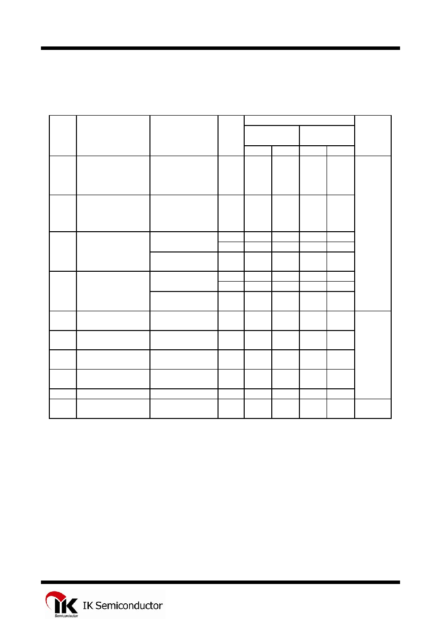
Absolute maximum conditions*
Parameter, unit
Symbol
Value
min
max
Supply voltage, V
V
CC
-0.5 7.0
Input voltage, V
Vin
-0.5
7.0
Output voltage, V
Vout
-0.5 V
CC
+ 0.5B
Output voltage, V
Vout1
-0.5
7.0
Input diode current, mA
Iik
-
-20
Current of common output and supply
output, mA
Icc
50
Output current, mA
Iout
25
Output diode current, mA
Iok
20
Dissipated power, mW
Pd
180
*Under absolute maximum conditions operation of microcircuit is not guaranteed. Operation is
guaranteed under maximum conditions
Maximum conditions
Symbol Value
Parameter, unit
min
max
Supply voltage, V
V
CC
4.5 5.5
Input voltage,V
Vin
0
V
CC
Output voltage, V
Vout
0
V
CC
Output voltage, V
Vout1
0
5.5*
Output current, mA
Iout
-
8.0
Input rise and fall time, ns/V
t
LH
, t
HL
0 20
* - Vcc = 0V
3
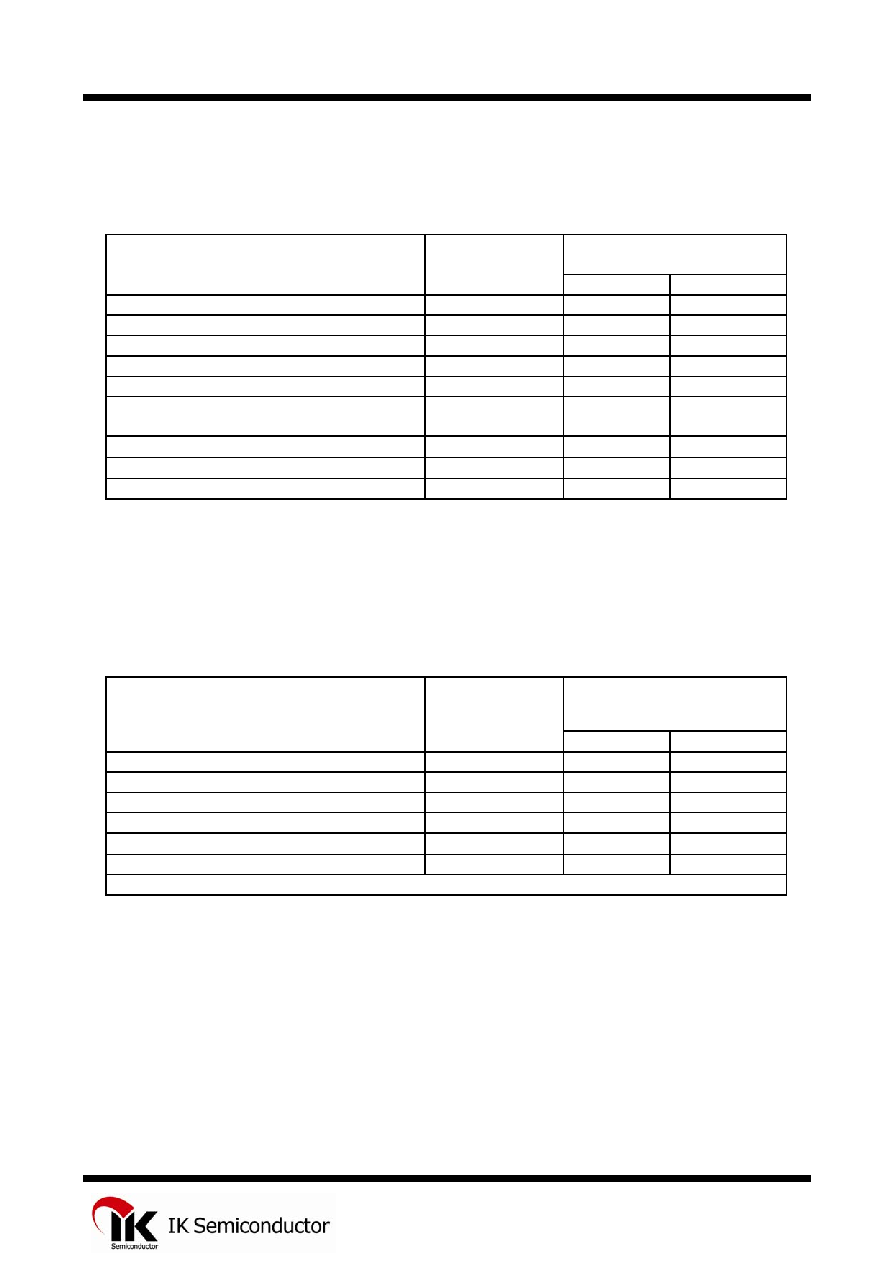
IN74VHCT74
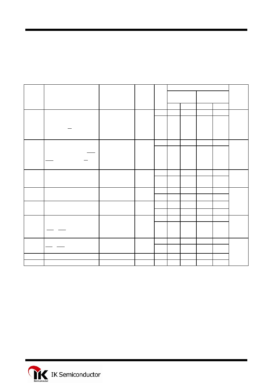
AC electrical characteristics (t
LH
= t
HL
= 3.0 ns)
Value
25
úC
-40
to 85
úC
Symbol Parameter
Test conditions
V
CC
, V
C
L
,
pF
min
max min max
Unit
15
- 7.8 - 9.0
t
PHL
,
t
PLH
Propagation delay time
when switching "on",
"off" from input —– to
outputs Q,
Q
V
IL
= 0 V,
V
IÕ
=3.0 V
,
5.0 0.5
50
- 8.8 - 10.0
ns
15
- 10.4 - 12.0
t
PHL
,
t
PLH
Propagation delay time
when switching "on",
"off" from inputs
SD
,
RD
to outputs Q,
Q
V
IL
= 0 V,
V
IÕ
=2.0 V
,
5.0 0.5
50
- 11.4 - 13.0
ns
15
- 100 - 80
f
max
Maximum Clock
Frequency
V
IL
= 0 V,
V
IÕ
=Vcc
,
5.0 0.5
50
- 80 - 65
MHz
15
5.0
- 5.0 -
t
SU
Time of setting signal D
to CP
V
IL
= 0 V,
V
IÕ
=Vcc
,
5.0 0.5
50
5.0
- 5.0 -
15
0 - 0 -
t
H
Retention time, D signal
to CP
V
IL
= 0 V,
V
IÕ
=Vcc
,
5.0 0.5
50
0 - 0 -
ns
15
3.5
- 3.5 -
t
REM
Time of recovery of
signal —– after signals
SD
,
RD
V
IL
= 0 V,
V
IÕ
=Vcc
,
5.0 0.5
50
3.5
- 3.5 -
15
5 - 5 -
t
W
Pulse duration of CP,
SD
,
RD
signals
V
IL
= 0 V,
V
IÕ
=Vcc
,
5.0 0.5
50
5 - 5 -
C
I
Input capacity
-
5.0
10
pF
C
–D
Dynamic capacity
V
I
= 0 V orV
CC
5.0 48
5