IN90S2313DW,
1
8-
BIT
M
ICROCONTROLLER WITH
2K
BYTES
B
UILD
-
IN
P
ROGRAMMABLE
F
LASH
Description
The IN90S2313 is a low-power CMOS 8-bit
microcontroller based on the AVR enhanced RISC
architecture. By executing powerful instructions in a single
clock cycle, the IN90S2313 achieves throughputs
approaching 1 MIPS per MHz allowing the system
designer to optimize power consumption versus
processing speed. The AVR core combines a rich
instruction set with 32 general purpose working registers.
All the 32 registers are directly connected to the
Arithmetic Logic Unit (ALU), allowing two independent
registers to be accessed in one single instruction
executed in one clock cycle. The resulting architecture is
more code efficient while achieving throughputs up to ten
times faster than conventional CISC microcontrollers.
The IN90S2313 provides the following features: 2K bytes of In-System Programmable
Flash, 128 bytes EEPROM, 128 bytes SRAM, 15 general purpose I/O lines, 32 general
purpose working registers, flexible timer/counters with compare modes, internal and
external interrupts, a programmable serial UART, programmable Watchdog Timer with
internal oscillator, an SPI serial port for Flash Memory downloading and two software
selectable power saving modes. The Idle Mode stops the CPU while allowing the SRAM,
timer/counters, SPI port and interrupt system to continue functioning. The power down
mode saves the register contents but freezes the oscillator, disabling all other chip
functions until the next interrupt or hardware reset. The device is manufactured using
Atmel's high density non-volatile memory technology. The on-chip In-System
Programmable Flash allows the program memory to be reprogrammed in-system
through an SPI serial interface or by a conventional nonvolatile memory programmer. By
combining an enhanced RISC 8-bit CPU with In-System Programmable Flash on a
monolithic chip, the Atmel IN90S2313 is a powerful microcontroller that provides a highly
flexible and cost effective solution to many embedded control applications.
The IN90S2313 AVR is supported with a full suite of program and system development
tools including: C compilers, macro assemblers, program debugger/simulators, in-circuit
emulators, and evaluation kits.

IN90S2313DW,
2
Features
ћ AVR - High Performance and Low Power RISC Architecture
ћ 118 Powerful Instructions - Most Single Clock Cycle Execution
ћ 2K bytes of In-System Reprogrammable Flash
- SPI Serial Interface for Program Downloading
- Endurance: 1,000 Write/Erase Cycles
ћ 128 bytes EEPROM
- Endurance: 100,000 Write/Erase Cycles
ћ 128 bytes Internal RAM
ћ 32 x 8 General Purpose Working Registers
ћ 15 Programmable I/O Lines
ћ V
CC
: 2.7 - 6.0V
ћ Fully Static Operation
- 0 - 10 MHz, 4.0 - 6.0V
- 0 - 4 MHz, 2.7 - 6.0V
ћ Up to 10 MIPS Throughput at 10 MHz
ћ One 8-Bit Timer/Counter with Separate Prescaler
ћ One 16-Bit Timer/Counter with Separate Prescaler and
Compare and Capture Modes
ћ Full Duplex UART
ћ Selectable 8, 9 or 10 bit PWM
ћ External and Internal Interrupt Sources
ћ Programmable Watchdog Timer with On-Chip Oscillator
ћ On-Chip Analog Comparator
ћ Low Power Idle and Power Down Modes
ћ Programming Lock for Software Security
ћ
20-Pin Device
IN90S2313DW,
3
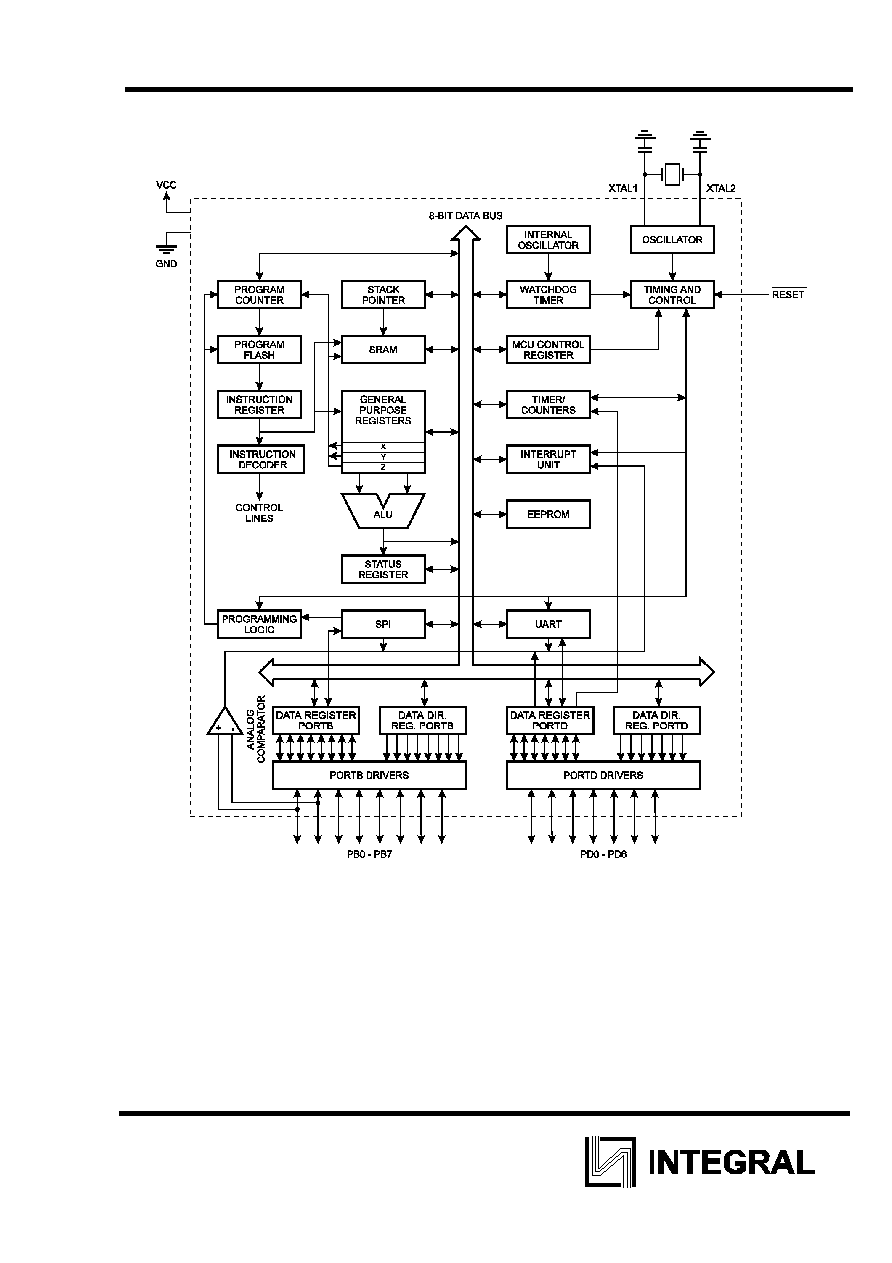
Block Diagram
IN90S2313DW,
4
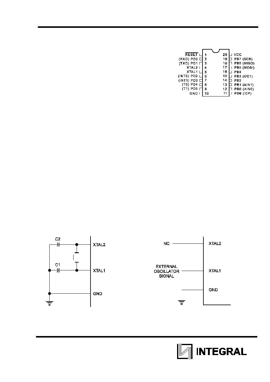
Pin Descriptions
VCC
Supply voltage pin.
GND
Ground pin.
Port B (PB7..PB0)
Port B is an 8-bit bi-directional I/O port. Port pins can provide
internal pull-up resistors (selected for each bit). PB0 and PB1
also serve as the positive input (AIN0) and the negative input
(AIN1), respectively, of the on-chip analog comparator. The Port
B output buffers can sink 20mA and can drive LED displays directly. When pins PB0 to PB7 are used as
inputs and are externally pulled low, they will source current if the internal pull-up resistors are activated.
Port B also serves the functions of various special features of the IN90S2313 as listed on page 38.
Port D (PD6..PD0)
Port D has seven bi-directional I/O pins with internal pull-up resistors, PD6..PD0. The Port D output
buffers can sink 20 mA. As inputs, Port D pins that are externally pulled low will source current if the pull-
up resistors are activated.
Port D also serves the functions of various special features of the IN90S2313 as listed on page 43.
RESET
Reset input. A low on this pin for two machine cycles while the oscillator is running resets the device.
XTAL1
Input to the inverting oscillator amplifier and input to the internal clock operating circuit.
XTAL2
Output from the inverting oscillator amplifier
Crystal Oscillator
XTAL1 and XTAL2 are input and output, respectively, of an inverting amplifier which can be configured for
use as an on-chip oscillator. Either a quartz crystal or a ceramic resonator may be used. To drive the
device from an external clock source, XTAL2 should be left unconnected while XTAL1 is driven.
Oscillator Connections
External Clock Drive Configuration

IN90S2313DW,
5
Architectural Overview
The fast-access register file concept contains 32 x 8-bit general purpose working registers with a single
clock cycle access time. This means that during one single clock cycle, one ALU (Arithmetic Logic Unit)
operation is executed. Two operands are output from the register file, the operation is executed, and the
result is stored back in the register file -in one clock cycle.
Six of the 32 registers can be used as three 16-bits indirect address register pointers for Data Space
addressing -enabling efficient address calculations. One of the three address pointers is also used as the
address pointer for the constant table look up function. These added function registers are the 16-bits X-
register, Y-register and Z-register. The ALU supports arithmetic and logic functions between registers or
between a constant and a register. Single register operations are also executed in the ALU.
In addition to the register operation, the conventional memory addressing modes can be used on the
register file as well. This is enabled by the fact that the register file is assigned the 32 lowermost Data
Space addresses ($00 -$1F), allowing them to be accessed as though they were ordinary memory
locations.
The I/O memory space contains 64 addresses for CPU peripheral functions as Control Registers,
Timer/Counters, A/D-converters, and other I/O functions. The I/O memory can be accessed directly, or as
the Data Space locations following those of the register file, $20 - $5F.
The AVR has Harvard architecture - with separate memories and buses for program and data. The
program memory is accessed with a two stage pipeline. While one instruction is being executed, the next
instruction is pre-fetched from the program memory. This concept enables instructions to be executed in
every clock cycle. The program memory is In-system Programmable Flash memory.
With the relative jump and call instructions, the whole 1K address space is directly accessed. Most AVR
instructions have a single 16-bit word format. Every program memory address contains a 16- or 32-bit
instruction.
During interrupts and subroutine calls, the return address program counter (PC) is stored on the stack.
The stack is effectively allocated in the general data SRAM, and consequently the stack size is only
limited by the total SRAM size and the usage of the SRAM. All user programs must initialize the SP in the
reset routine (before subroutines or interrupts are executed). The 8-bit stack pointer SP is read/write
accessible in the I/O space.
The 128 bytes data SRAM + register file and I/O registers can be easily accessed through the five
different addressing modes supported in the AVR architecture.
The memory spaces in the AVR architecture are all linear and regular memory maps.