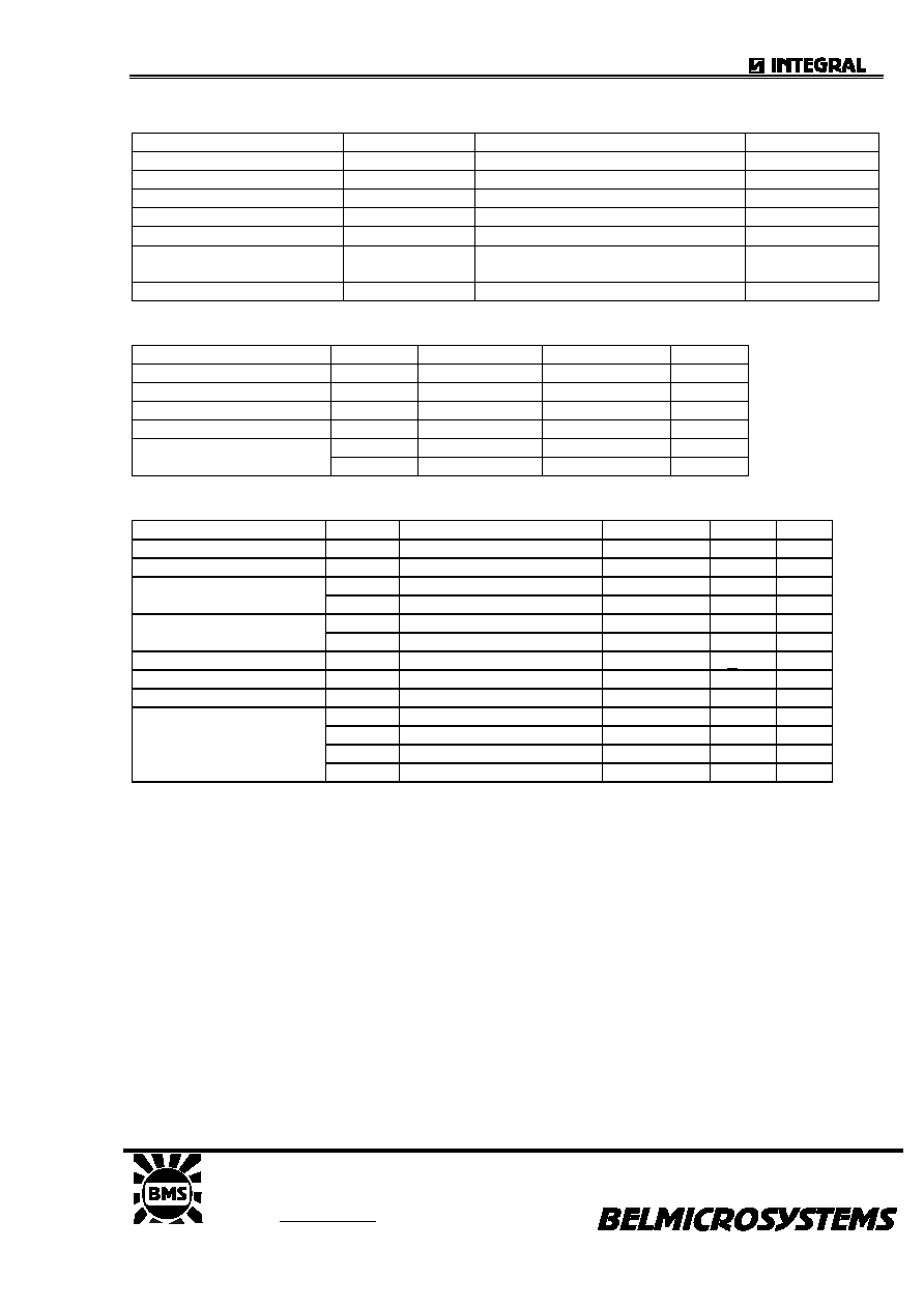
 | –≠–ª–µ–∫—Ç—Ä–æ–Ω–Ω—ã–π –∫–æ–º–ø–æ–Ω–µ–Ω—Ç: IND16337 | –°–∫–∞—á–∞—Ç—å:  PDF PDF  ZIP ZIP |

IND16337
Korzhenevsky 12, Minsk, 220064, Republic of Belarus
Fax: +375 (17) 278 28 22
Tel: +375 (17) 278 49 09, 212 27 02
Tel/fax: +375 (17) 212 68 53
E-mail: office@bms.by
URL: www.bms.by
1
64-BIT AC-PDP DRIVER
The IND16337 is a high-voltage CMOS driver designed for flat display panels such as
PDPs, VFDs and ELs. It consists of a 64-bit bi-directional shift register (16 bit 4
circuits), 64-bit latch and high-voltage CMOS driver. The logic block is designed to
operate at 5-V power supply, enabling direct connection to a microcontroller. In addition,
the IND16337 achieves low power dissipation by employing CMOS structure while having
a high withstand voltage output (150 V, 40 mA MAX.)
FEATURES
û Built in four 16-bit bi-directional shift register circuits
û Data control with transfer clock (external) and latch
û High-speed data transfer (fmax. = 20 MHz MIN. at cascade connection)
û Wide operating temperature range (TA = -40 to +85
o
C)
û High withstand output voltage (150 V, 40 mA MAX.)
û 5-V CMOS input interface
û High withstand voltage CMOS structure
û Capable of reversing all driver outputs by PC pin
BLOCK DIAGRAM
Note High withstand voltage CMOS driver, 150 V, +40 mA (MAX.)
S
1
S
5
S
61
I/O
I/O
Sr1
S
2
S
6
S
62
Sr2
S
3
S
7
S
63
Sr3
S
4
S
8
S
64
Sr4
O
6
O
1
L
1
S
64
S
63
S
62
S
61
S
4
S
3
S
2
S
1
PC
BLK
LE
A
1
CLK
R/L
B
1
A
2
B
2
A
3
B
3
A
4
B
4
Note
I/O
I/O
I/O
I/O
I/O
I/O

IND16337
Korzhenevsky 12, Minsk, 220064, Republic of Belarus
Fax: +375 (17) 278 28 22
Tel: +375 (17) 278 49 09, 212 27 02
Tel/fax: +375 (17) 212 68 53
E-mail: office@bms.by
URL: www.bms.by
2
PIN CONFIGURATION (Top View)
Cautions
1. Pin 40 is connected to the lead frame, and therefore must be left open.
2. Ensure that the V
DD1
, V
DD2
, V
SS1
and V
SS2
pins are all used, and that V
SS1
and V
SS2
are used at the
same potential.
3. To prevent latch up breakdown, the power should be turned on in the order V
DD1
, logic signal, V
DD2
.
It should be turned off in the opposite order.
100-pin plaxtic QFP
100 99 98 97 96 95 94 93 92 91 90 89 88 87 86 85 84 83 82 81
80
79
78
77
76
75
74
73
72
71
70
68
67
66
65
64
63
62
61
60
59
58
57
69
56
55
54
53
52
51
31 32 33 34 35 36 37 38 39 40 41 42 43 44 45 46 47 48 49 50
1
3
4
5
6
7
8
9
10
11
13
14
15
16
17
19
20
21
22
23
24
12
25
26
27
28
29
30
NC
V
dd2
NC
V
ss2
NC
O
43
O
44
O
45
O
46
O
47
O
48
O
49
O
50
O
51
O
52
O
53
O
54
O
55
O
56
O
57
O
59
O
60
O
61
O
62
O
63
O
64
O
60
O
58
NC
NC
V
dd2
NC
NC
V
dd2
NC
V
ss2
NC
O
43
O
44
O
45
O
46
O
47
O
48
O
49
O
50
O
51
O
52
O
53
O
54
O
55
O
56
O
57
O
59
O
60
O
61
O
62
O
63
O
64
O
60
O
58
NC
NC
V
dd2
NC
O
42
O
41
O
40
O
39
O
38
O
37
O
36
O
35
O
34
O
33
O
32
O
31
O
30
O
29
O
28
O
26
O
25
O
24
O
23
O
27
LE
B
4
V
ss2
NC
CLK
B
3
B
2
B
1
V
ss1
NC
R/L
V
dd
1
A
1
A
2
A
3
A
4
PC
BL
K
NC
V
ss2

IND16337
Korzhenevsky 12, Minsk, 220064, Republic of Belarus
Fax: +375 (17) 278 28 22
Tel: +375 (17) 278 49 09, 212 27 02
Tel/fax: +375 (17) 212 68 53
E-mail: office@bms.by
URL: www.bms.by
3
PIN DESCRIPTION
Symbol
Pin Name
Pin Number Description
PC
Polarity change input
47
PC = L: All driver output invert
BLK
Blank input
48
BLK = H: All output = H or L
LE
Latch enable input
34
Automatically executes latch by setting High at rising
edgeof the clock
A1 to A4 RIGHT data input/output 43 to 46
B1 to B4 LEFT data input/output
38 to 35
When R/L = H,
A1 to A4: Input B1 to B4: Output
When R/L = L,
A1 to A4: Output B1 to B4:Input
CLK
Clock input
33
Shift executed on fall
R/L
Shift control input
41
Right shift mode when R/L = H
SR1: A1
S1 ûûû S61 B1
(Same direction for SR2ûSR4)
Left shift mode when R/L = L
SR1: B1
S61 ûûû S1 A1
(Same direction for SR2ûSR4)
O1 to O64 High withstand voltage
output
54 to 75, 81 to
100, 6 to 27
130 V, 40 mA MAX.
V
DD1
Power supply for logic
block
42
5 V +10%
V
DD2
Power supply for driver
block
2, 29, 52, 79 30 to 130 V
V
SS1
Logic GND
39
Connect to system GND
V
SS2
Driver GND
4, 31, 50, 77 Connect to system GND
NC
Non-connection
1, 3, 5, 28, 30,
32, 40, 49, 51,
53, 76, 78, 80
Non-connection
Ensure that pin 40 is left open.
TRUTH TABLE 1 (Shift Register Block)
Input Output Shift
Register
R/L CLK
A
B
H
Output
Note 1
Right shift execution
H
H or L
Input
Output Hold
L
Output
Note 2
Input
Left shift execution
L
H or L Output
Hold
Notes 1. The data of S57, S58, S59, S60 shifts to S61, S62, S63, S64 and is output from B1, B2, B3, B4 at
the falling edge of the clock, respectively.
2.
The data of S5, S6, S7, S8 shifts to S1, S2, S3, S4 and is output from A1, A2, A3, A4 at the
falling edge of the clock, respectively.
TRUTH TABLE 2 (Latch Block)
LE
CLK
Output State of Latch Block (Ln)
Latch Sn data and hold output data
H
Hold latch data
L
X
Hold latch data

IND16337
Korzhenevsky 12, Minsk, 220064, Republic of Belarus
Fax: +375 (17) 278 28 22
Tel: +375 (17) 278 49 09, 212 27 02
Tel/fax: +375 (17) 212 68 53
E-mail: office@bms.by
URL: www.bms.by
4
TRUTH TABLE 3 (Driver Block)
Ln
BLK
PC
Output State of Driver Block
X
H
H
H (All driver outputs: H)
X
H
L
L (All driver outputs: L)
X
L
H
Output latch data (Ln)
X
L
L
Output reversed latch data (Ln)
X: H or L, H: High level, L: Low level
TIMING CHART (Right shift)
Remark Values in parentheses in the above chart are when R/L = L.
CLK
A (B )
1 4
A (B )
2 3
A (B )
3 2
A (B )
4 1
S (S )
1 64
S (S )
2 63
S (S )
3 62
S (S )
4 61
S (S )
5 60
S (S )
6 59
S (S )
7 58
S (S )
8 57
BLK
LE
PC
O (O )
1 64
O (O )
2 63
O (O )
3 62
O (O )
4 61
O (O )
5 60
O (O )
6 59
O (O )
7 58
O (O )
8 57
IND16337
Korzhenevsky 12, Minsk, 220064, Republic of Belarus
Fax: +375 (17) 278 28 22
Tel: +375 (17) 278 49 09, 212 27 02
Tel/fax: +375 (17) 212 68 53
E-mail: office@bms.by
URL: www.bms.by
5
ABSOLUTE MAXIMUM RATINGS (T
A
= 25
o
C, V
SS1
= V
SS2
= 0 V)
Parameter Symbol
Ratings
Unit
Logic Block Supply Voltage
V
DD1
-0.5 to +7.0
V
Driver Block Supply Voltage
V
DD2
-0.5 to +150
V
Logic Block Input Voltage
V
I
-0.5 to V
DD1
+ 0.5
V
Driver Block Output Current
I
O2
40 mA
Power Dissipation
P
D
1300
Note
mW
Operating Ambient
Temperature
T
A
-40 to +85
o
C
Storage Temperature
Tstg
-65 to +150
o
C
Note Derate at -13 mW/
o
C at T
A
= 25
o
C or higher
RECOMMENDED OPERATING CONDITIONS (T
A
= -40 to +85
o
C, V
SS1
= V
SS2
= 0 V)
Parameter Symbol
MIN.
MAX.
Unit
Logic Block Supply Voltage
V
DD1
4.5
5.5 V
Driver Block Supply Voltage
V
DD2
30
130 V
High-Level Input Voltage
V
IH
0.8
V
DD1
V
DD1
V
Low-Level Input Voltage
V
IL
0 0.2
V
DD1
V
I
OH2
-30
mA
Driver Output Current
I
OL2
+30
mA
ELECTRICAL SPECIFICATIONS
(T
A
= 25
o
C, V
DD1
= 5.0 V, V
DD2
= 130 V, V
SS1
= V
SS2
= 0 V)
Parameter Symbol Condition
MIN.
MAX.
Unit
High-Level Output Voltage
V
OH1
Logic,
I
OH1
= -1.0 mA
0.9 V
DD1
V
DD1
V
Low-Level Output Voltage
V
OL1
Logic,
I
OL1
= 1.0 mA
0
0.1 V
DD1
V
V
OH21
O
1
to O
64
, I
OH2
= -10 mA
123
V
High-Level Output Voltage
V
OH22
O
1
to O
64
, I
OH2
= -30 mA
110
V
V
OL21
O
1
to O
64
, I
OL2
= 10 mA
5.0
V
Low-Level Output Voltage
V
OL22
O
1
to O
64
, I
OL2
= 30 mA
15
V
Input Leakage Current
I
IL
V
1
= V
DD1
or V
SS1
+1.0 uA
High-Level Input Voltage
V
IH
0.8
V
DD1
V
Low-Level Input Voltage
V
IL
0.2
V
DD1
V
I
DD1
Logic,
T
A
= -40 to +85
o
C
100
uA
I
DD1
Logic,
T
A
= 25
o
C
10
uA
I
DD2
Driver,
T
A
= -40 to +85
o
C
1000
uA
Static Current Dissipation
I
DD2
Driver,
T
A
= 25
o
C
100
uA