 | –≠–ª–µ–∫—Ç—Ä–æ–Ω–Ω—ã–π –∫–æ–º–ø–æ–Ω–µ–Ω—Ç: INF8582E | –°–∫–∞—á–∞—Ç—å:  PDF PDF  ZIP ZIP |
INF8582E
1
256
’
8
BIT
S
TATIC
C
MOS
EEPROM
WITH
I
2
—-
BUS
.
(
ANALOG
-
MICROCIRCUIT
PCF8582≈,
F
.P
HILIPS
).
INF8582E - 2 bit (256ı8 bit) electronically erasable programmable ROM with
"floating" gate. Internal reduntant code correcting errors as single bit errors is used to
enhance the reliability. Microcircuit operates in systems with serial I
2
C-bus consisting of
two lines: for data signals (SDA) (bidirectional) and for clock signals (SCL). Up to 8 mi-
crocircuits may be connected to I
2
C-bus. Stacker programming is done by tunneling
electrons. Programming voltage is generated by voltage multiplier built-in chip. The im-
plementation of CMOS technology in full provides low power consumption.
These products are purposed for implementation in portable consumer applica-
tions, in autoelectronics, in peripheric computer devices. Thea are used in TV chan-
nel selectors, for storage of frequency, volume and image data, in tuning control blocks
in radioset, , in measuring devices for standard curves storage, calibration data,
minimum and maximum values, in , seat position adgusting systems, side glass, in
speedometers.
Characteristic properties:
- without decay storage 2 bit 10 years;
- single-error correction circuit;
- one power supply (UÒÒ=4,5V - 5,5V);
- built-in voltage multiplier in chip;
- input/output consecutive bus ;
- automatic increment of word address;
- internal timer for recording;
- 100 000 cycles erasure/recording on byte with low failure rate;
- unlimited number of reading cycles;
- low power consumption;
- temperature range -40 - +85
Œ
—.
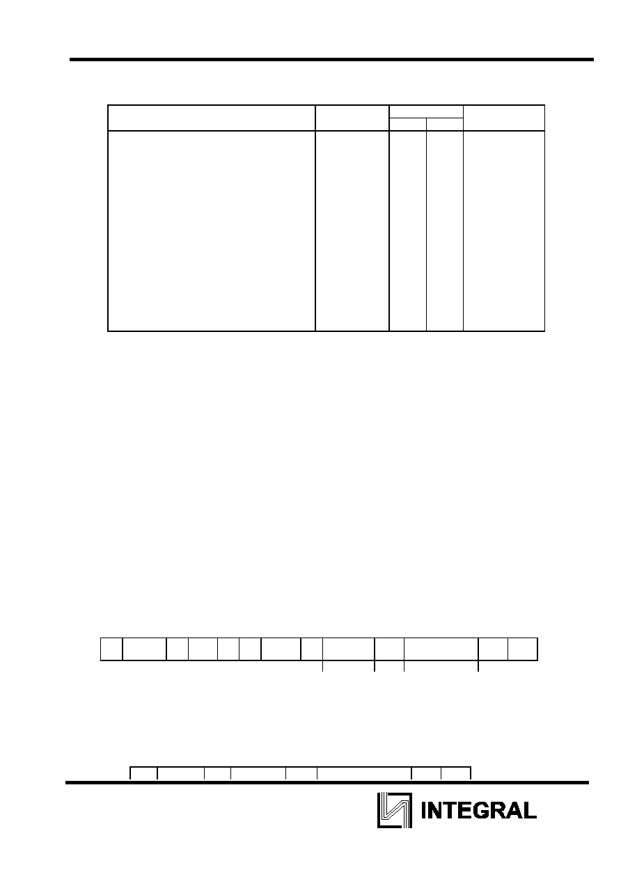
The basing circuit diagram and Pins purpose table are given below in fig.1, main
electrical characteristics are indicated in Table 1.
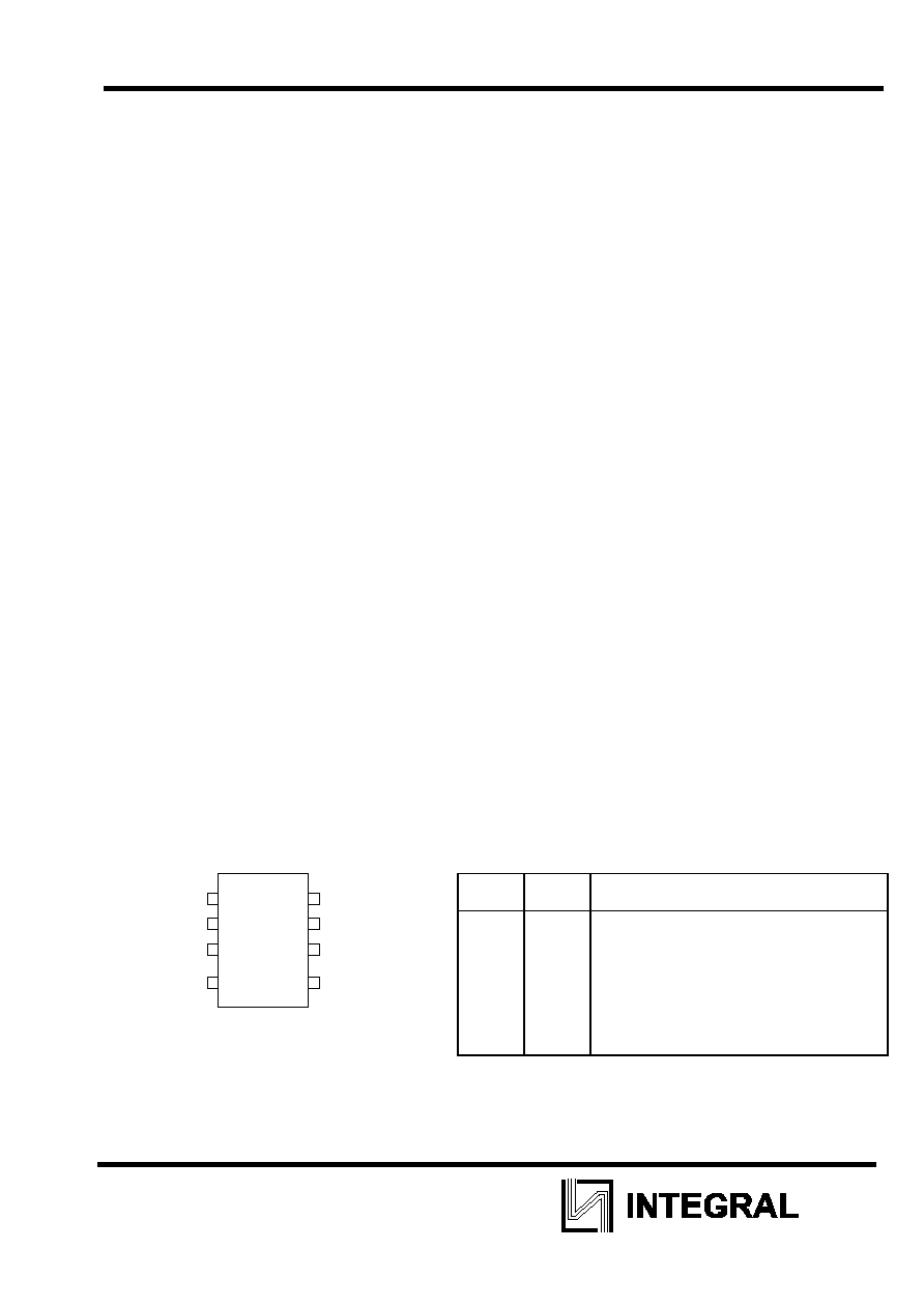
Microcircuit basing diagram
Pins purpose table
Pin Sym-
bol
Purpose
1
2
3
4
5
6
7
8
A0
A1
A2
Uss
SDA
SCL
“≈S“
Ucc
address input
address input
address input
"ground"
data line, input/output
clock signal line (input)
synchronizing signal of programming
power supply
–ËÒ.1
¿
¿
¿
Uss
Ucc
TEST
SCL
SDA
1
2
3
4
8
7
6
5
Package: 2101.8-A
INF8582E
2
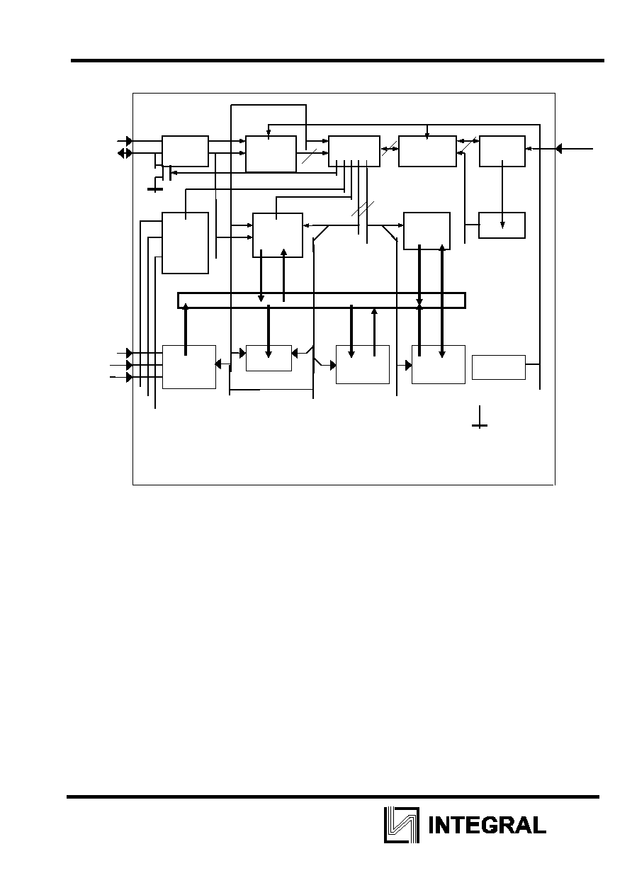
BLOCK DIAGRAM
PTC
SCL(6)
SDA(5)
A0(1)
A1(2)
A2(3)
GND(4)
INPUT
FILTER
ADDRESS
HIGH
REGISTER
I
2
C-BUS
CONTROL
LOGIC
DDRESS
HIGH
REGISTER 1
TIMER
ADDRESS
SWITCH
SHIFT
REGISTER
BYTE
LATCH
DIVIDER
(/128)
TEST MODE
DECODER
ADDRESS
POINTER
EEPROM
TEST MODE
DECODER 1
POWER-ON
RESET
INTERNAL BUS
(7)
INF8582E
3
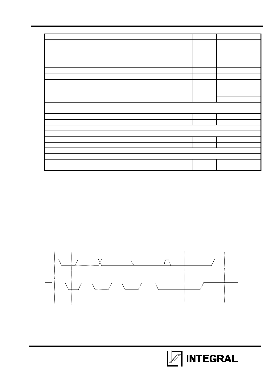
Table 1 - Main characteristics of microcircuits
Parameters Mode
Symbol
Min
Max
Dynamic consumption current (reading), mA
f
SCL
=100ÍHz
U
CC
=5.5V
I
CC0(RD)
-
1,6
Dynamic consumption current(erasure/recording),
m¿
f
SCL
=100ÍHz
U
CC
=5.5V
I
CC0(E/WR)
-
2,5
Supply voltage, V
V
DD
4.5
5.5
Static consumption current,
¿
U
CC
=5,5V I
CCS
- 10,0
Clock frequency, ÍHz
f
SCL
0 100
Max output current, m¿
I
ŒL
3.0
Duration of " erasure/recording " cycle, ms:
- input external control TEST
t
E/WR
5
25
- inside chip control
10
ü 13 (standard)
Input “≈S“
High level input voltage, V
U
IH
0,9U
CC
U
CC
+0,8
Low level input voltage, V
U
IL
-0,8
0,1U
CC
InputsSCL and SDA
High level input voltage, V
U
IH
0,7U
CC
U
CC
+0,8
Low level input voltage, V
U
IL
-0,8
0,3U
CC
Output SDA
Low level output voltage, V
I
OL
=3,0 mA
U
CC
=4,5 V
U
OL
- 0,4
In order to make the understanding of the microcircuit INF8582E way of operation easier it
is necessary to examine I
2
C-bus interface characteristics.
I
2
C-bus is a bidirectional double-wire serial bus purposed for data exchange between dif-
ferent (various) integrated circuits. It consists of date line (SDA) and clock signals line (SCL). In
common case the both lines should be connected to the positive power supply by charging re-
sistor (output stage with open drain/collector). As for the designed product, only SDA line (in-
put/output) is bidirectional therefore charging resistor on SCL line is not necessary. Resistor
nominal value is limited at the bottom - by load capability of microcircuit (I
OL
=3,0 mA), at the
top - by the build-up font duration (t
R
=1,0 s). Operation of the microcurcuit is stable within the
resistance range from 1,5 kOhm up to 10 kOhm. The possible operation modes of I
2
C-bus are
showed in figure 2.
Operation modes of I
2
—-bus
bus is condition
Data transmission with acknowledgment bit
condition "stop", bus
free "start",
end of transmission
is free
start of
ransmission
Fig. 2
Input
Input
Output
Input
ST
SP
SDA
SCL
1
8
9
INF8582E
4
The following modes of I
2
—-bus are defined:
- bus is free (not engaged) - both lines are in "high" mode;
- transmission start (condition "Start") - passing of the line SDA from "high" level to
"low" when SCL is in "high" mode;
- data transmission;
- end of transmission (condition "Stop") - passing of the line SDA from "low" level to
"high" while the line SCL is in "high" mode.
The data transmission can start only when the bus is free. During the data transmission
the data line must be stable all the time while clock line is "high". The SDA line mode can
change only when the clock signals line SCL is in "low" mode. One clock signal falls at one data
bit. The change in SDA line mode when Clock line is "high" will be interpreted as check signals:
"Start" or "Stop".
Each transmission of data starts with the condition "Start" and is finished with the condition
"Stop". The information is always transmitted in bytes. The number of data bytes transmitted be-
tween the conditions "Start" and "Stop" is limited in "Erasure/recording" mode and not limited in
"Reading" mode. Each word of 8 bits (each byte) is accompanied by the 9
th
test bit, acknowl-
edgment bit. This bit is always generated on SDA line by the device which received the previous
data byte (i.e. "receiver"). The device acknowledging the receipt of the data (if it meets the re-
quirements), rarefies the SDA line so that this line is constantly "low" during all period of "high"
level of clock acknowledgment pulse (9
th
bit) on SCL line. The device transmitting the data dur-
ing acknowledgment forming must take the mode with high output resistance. If the received
data byte does not comply with the requirements, the receiving device does not generate the
acknowledgment which indicates to the error in exchange protocol on I
2
—-bus.
All devices connected to I
2
—-bus may be devided in two groups: main devices which
control the data transmission along the bus (microcontrollers, microprocessors), and subordi-
nate devices, which are controlled by main devices (service and peripheric devices). In their
turn the both groupsof devices may be as receivers (devices receiving the data at that mo-
ment) and transmitters (devices transmitting the data the bus). The designed microcircuit
INF8582E may be only subordinate receiver or subordinate transmitter.The time diagram of
I
2
—-bus is showed in fig.3. Signal parameters of I
2
—-bus time diagram are given in table 2.
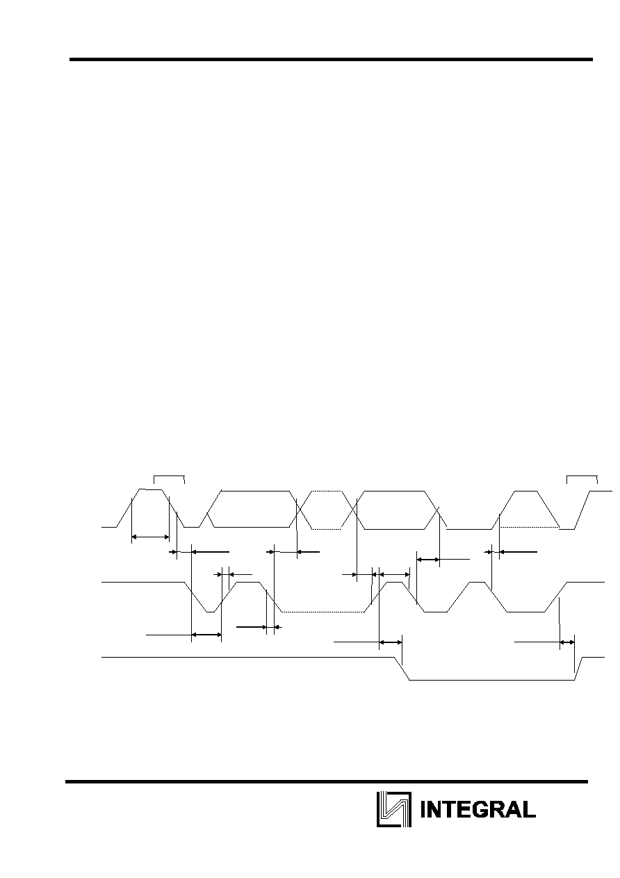
I
2
—-bus time diagram
Fig. 3
SDA
SCL
SDA
t
BUF
t
HD, STA
t
R
1
t
LOW
t
F
T
HD
.
DAT
8
9
T
SU
.
STA
T
SU
.
STO
T
HD
.
ACK
T
SU
.
ACK
t
HIGH
T
SU
.
DAT
INF8582E
5
Table 2 Signal parameters on I
2
—-bus
Parameter name,
Symbol
Value
Notes
unit of the measurement
min
max
Time when the bus is free before genera-
tion of start condition,
s
t
BUF
4.7
-
Conditionstart set up time,
s
T
SU
.
STA
4.7
- 1
Condition start retention time,
s
t
HD
.
STA
4.0
-
Low period of clock signal,
s
t
LOW
4.5
-
High period of clock signal,
s
t
HIGH
4.0
-
Rise front duration, ns
t
R
-
1.0
Fall front duration, ns
t
F
-
300.
0
Data retention time,ns
t
HD
.
DAT
0
-
2
Data retention time,
s
t
HD
.
DAT
5.0
-
3
Data set up time, ns
t
SU
.
DAT
250.
0
-
Acknowledgment generation time,
s
t
SU
.
ACK
-
3.5
Acknowledgment retention time,
s
t
HD
.
ACK
0
-
Condition Stop set up time,
s
t
HD
.
STO
4.7
-
Notes: 1. For repeated start.
2. Microcircuit INF8582E is a "subordinate transmitter".
3.Microcircuit INF8582E is a "subordinate receiver".
Among the parameters stipulated in table 2 the particular attention should be paid to set up
and data retention time. Two modes should be considered.
The first mode.
œÂ‚˚È ÂÊËÏ. Microcircuit INF8582E receive data, i.e. is a "subordinate receiver. In this
case time t
SU.DAT
and t
HD.DAT
must be garanteed by "main transmitter". "Latchup" of data being re-
ceived in microcircuit is effected onback front of clock pulse.
The second mode. Microcircuit INF8582E generate a data which goes to the line SDA,
i.e.. is a " subordinate transmitter". In this case time t
SU.DAT
and t
HD.DAT
are determined by the mi-
crocircuit parameters. True information on the line SDA is set by back front of the previous clock
pulse. In other words, usefull information is already on the leading edge of the next clock pulse
on the line SDA.
The protocols of I
2
C -bus for all microcircuits operating modes are shown in fig. 4-6, in fig.7
- time diagram of signals on the bus in the mode erasure/recording using external master os-
cillator. The signal parameters in the mode erasure/recording are stated in table 3, in tables
4,5 - interpretation of key words and symbols, used for presentation of these protocols.
I
2
—-bus protocol in the Reading mode with input of word address
S
T
CS/WR A
s
WA A
s
S
T
CS/R
D
A
s
DA Am
DA
Am
SP
n
bytes last
byte
automatic increment of word being read-out
Fig. 4
I
2
—-bus short protocol in the mode "Reading"
ST CS/RD As DA
Am DA
Am SP