 | –≠–ª–µ–∫—Ç—Ä–æ–Ω–Ω—ã–π –∫–æ–º–ø–æ–Ω–µ–Ω—Ç: IW4015BD | –°–∫–∞—á–∞—Ç—å:  PDF PDF  ZIP ZIP |

TECHNICAL DATA
24
Dual 4-Stage Static Shift Register
High-Voltage Silicon-Gate CMOS
The IW4015B consists of two identical, independent, 4-stage
serial-input/parallel-output registers. Each register has independent
CLOCK and RESET inputs as well as a single serial DATA input. "Q"
outputs are available from each of the four stages on both registers. All
register stages are D-type, master-slave flip-flops. The logic level
present at the DATA input is transferred into the first register stage and
shifted over one stage at each positive-going clock transition. Resetting
of all stages is accomplished by a high level on the reset line. Register
expansion to 8 stages using one IW4015B package, or to more than 8
stages using additional IW4015B's is possible.
û
Operating Voltage Range: 3.0 to 18 V
û
Maximum input current of 1
A at 18 V over full package-
temperature range; 100 nA at 18 V and 25
ú
C
û
Noise margin (over full package temperature range):
1.0 V min @ 5.0 V supply
2.0 V min @ 10.0 V supply
2.5 V min @ 15.0 V supply
IW4015B
ORDERING INFORMATION
IW4015BN Plastic
IW4015BD SOIC
T
A
= -55
ú
to 125
ú
C for all packages
PIN ASSIGNMENT
FUNCTION TABLE
Inputs
Outputs
Clock
Data
Reset
Q1
Q
n
L
L
L
Q
n-1
H
L
H
Q
n-1
X
L
No change
X
X
H
L
L
X = don't care
LOGIC DIAGRAM
PIN 16=V
CC
PIN 8= GND

IW4015B
25
MAXIMUM RATINGS
*
Symbol
Parameter
Value
Unit
V
CC
DC Supply Voltage (Referenced to GND)
-0.5 to +20
V
V
IN
DC Input Voltage (Referenced to GND)
-0.5 to V
CC
+0.5
V
V
OUT
DC Output Voltage (Referenced to GND)
-0.5 to V
CC
+0.5
V
I
IN
DC Input Current, per Pin
10
mA
P
D
Power Dissipation in Still Air, Plastic DIP+
SOIC Package+
750
500
mW
P
D
Power Dissipation per Output Transistor
100
mW
Tstg
Storage Temperature
-65 to +150
ú
C
T
L
Lead Temperature, 1 mm from Case for 10 Seconds
(Plastic DIP or SOIC Package)
260
ú
C
*
Maximum Ratings are those values beyond which damage to the device may occur.
Functional operation should be restricted to the Recommended Operating Conditions.
+Derating - Plastic DIP: - 10 mW/
ú
C from 65
ú
to 125
ú
C
SOIC Package: : - 7 mW/
ú
C from 65
ú
to 125
ú
C
RECOMMENDED OPERATING CONDITIONS
Symbol
Parameter
Min
Max
Unit
V
CC
DC Supply Voltage (Referenced to GND)
3.0
18
V
V
IN
, V
OUT
DC Input Voltage, Output Voltage (Referenced to GND)
0
V
CC
V
T
A
Operating Temperature, All Package Types
-55
+125
ú
C
This device contains protection circuitry to guard against damage due to high static voltages or electric
fields. However, precautions must be taken to avoid applications of any voltage higher than maximum rated
voltages to this high-impedance circuit. For proper operation, V
IN
and V
OUT
should be constrained to the range
GND
ò
(V
IN
or V
OUT
)
ò
V
CC
.
Unused inputs must always be tied to an appropriate logic voltage level (e.g., either GND or V
CC
).
Unused outputs must be left open.
IW4015B
26
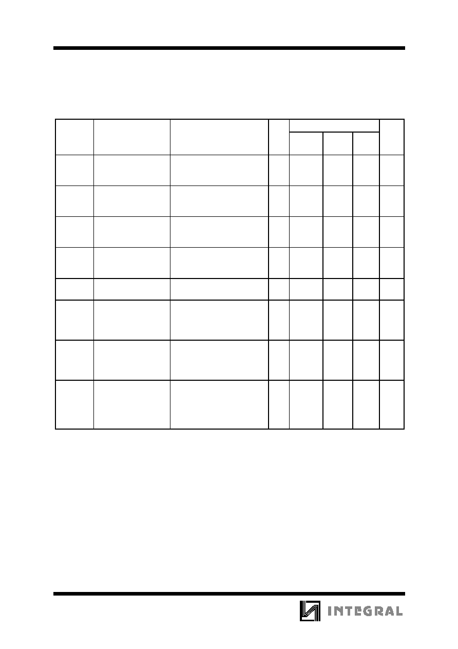
DC ELECTRICAL CHARACTERISTICS
(Voltages Referenced to GND)
V
CC
Guaranteed Limit
Symbol
Parameter
Test Conditions
V
ô
-55
ú
C
25
ú
C
ò
125
ú
C
Unit
V
IH
Minimum High-Level
Input Voltage
V
OUT
= 0.5 V or V
CC
- 0.5V
V
OUT
= 1.0 V or V
CC
- 1.0 V
V
OUT
= 1.5 V or V
CC
- 1.5V
5.0
10
15
3.5
7
11
3.5
7
11
3.5
7
11
V
V
IL
Maximum Low -Level
Input Voltage
V
OUT
= 0.5 V or V
CC
- 0.5V
V
OUT
= 1.0 V or V
CC
- 1.0 V
V
OUT
= 1.5 V or V
CC
- 1.5V
5.0
10
15
1.5
3
4
1.5
3
4
1.5
3
4
V
V
OH
Minimum High-Level
Output Voltage
V
IN
=GND or V
CC
5.0
10
15
4.95
9.95
14.95
4.95
9.95
14.95
4.95
9.95
14.95
V
V
OL
Maximum Low-Level
Output Voltage
V
IN
=GND or V
CC
5.0
10
15
0.05
0.05
0.05
0.05
0.05
0.05
0.05
0.05
0.05
V
I
IN
Maximum Input
Leakage Current
V
IN
= GND or V
CC
18
0.1
0.1
1.0
A
I
CC
Maximum Quiescent
Supply Current
(per Package)
V
IN
= GND or V
CC
5.0
10
15
20
5
10
20
100
5
10
20
100
150
300
600
3000
A
I
OL
Minimum Output Low
(Sink) Current
V
IN
= GND or V
CC
U
OL
=0.4 V
U
OL
=0.5 V
U
OL
=1.5 V
5.0
10
15
0.64
1.6
4.2
0.51
1.3
3.4
0.36
0.9
2.4
mA
I
OH
Minimum Output
High (Source) Current
V
IN
= GND or V
CC
U
OH
=2.5 V
U
OH
=4.6 V
U
OH
=9.5 V
U
OH
=13.5 V
5.0
5.0
10
15
-2
-0.64
-1.6
-4.2
-1.6
-0.51
-1.3
-3.4
-1.15
-0.36
-0.9
-2.4
mA
IW4015B
27
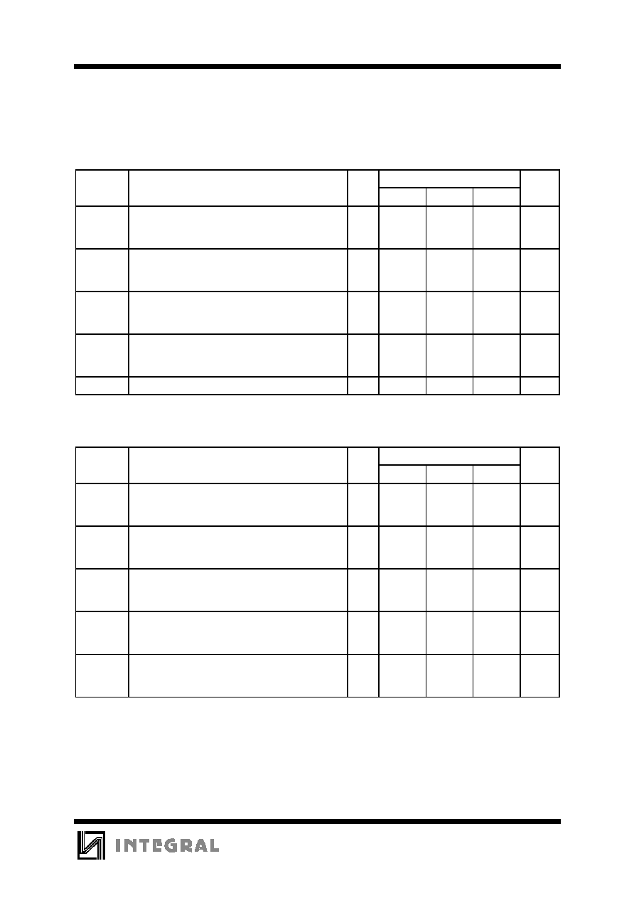
AC ELECTRICAL CHARACTERISTICS
(C
L
=50pF, R
L
=200k
, Input t
r
=t
f
=20 ns)
V
CC
Guaranteed Limit
Symbol
Parameter
V
ô
-55
ú
C
25
ú
C
ò
125
ú
C
Unit
t
max
Maximum Clock Frequency (Figure 1)
5.0
10
15
3
6
8.5
3
6
8.5
1.5
3
4.25
MHz
t
PHL
, t
PLH
Maximum Propagation Delay, Clock to Q
(Figure 1)
5.0
10
15
320
160
120
320
160
120
640
320
240
ns
t
PHL
Maximum Propagation Delay, Reset to Q
(Figure 2)
5.0
10
15
400
200
160
400
200
160
800
400
320
ns
t
THL
, t
TLH
Maximum Output Transition Time, Any Output
(Figure 1)
5.0
10
15
200
100
80
200
100
80
400
200
160
ns
C
IN
Maximum Input Capacitance
-
7.5
pF
TIMING REQUIREMENTS
(C
L
=50pF, R
L
=200 k
, Input t
r
=t
f
=20 ns)
V
CC
Guaranteed Limit
Symbol
Parameter
V
ô
-55
ú
C
25
ú
C
ò
125
ú
C
Unit
t
w
Minimum Pulse Width, Clock (Figure 1)
5.0
10
15
180
80
50
180
80
50
360
160
100
ns
t
w
Minimum Pulse Width, Reset (Figure 2)
5.0
10
15
200
80
60
200
80
60
400
160
120
ns
t
su
Minimum Setup Time, Data to Clock
(Figure 3)
5.0
10
15
70
40
30
70
40
30
140
80
60
ns
t
h
Minimum Hold Time, Clock to Data
(Figure 3)
5.0
10
15
0
0
0
0
0
0
0
0
0
ns
t
r
, t
f
Maximum Input Rise and Fall Time (Figure 1)
5.0
10
15
15
6
2
15
6
2
30
12
4
s
IW4015B
28
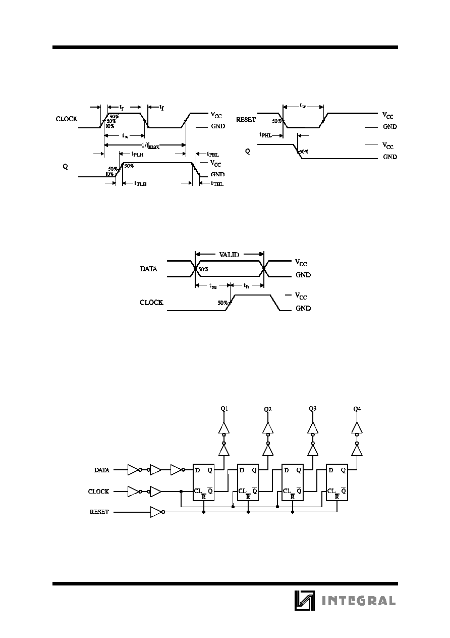
Figure 1. Switching Waveforms
Figure 2. Switching Waveforms
Figure 3. Switching Waveforms
EXPANDED LOGIC DIAGRAM
( 1/2 of the Device)