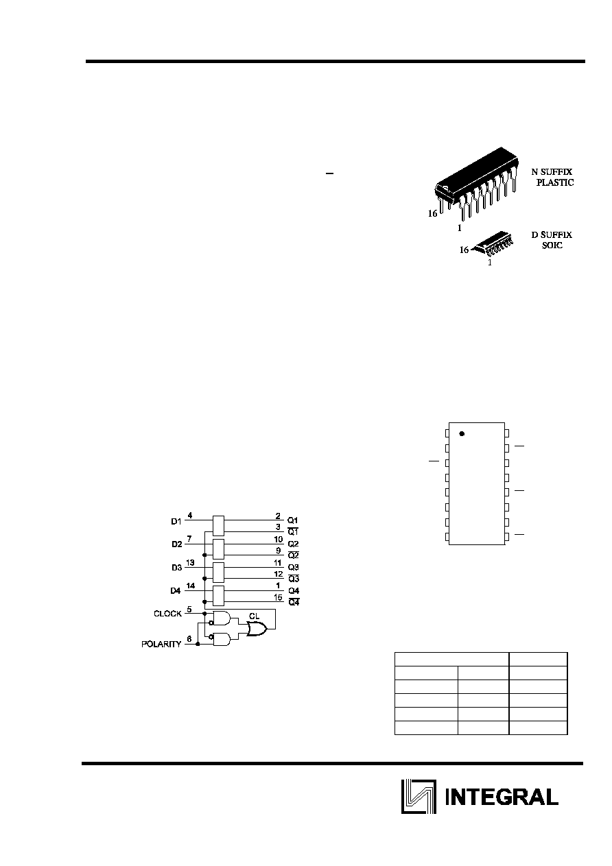
IW4042B
1
Q
UAD
C
LOCKED
D
L
ATCH
High-Voltage Silicon-Gate CMOS
CD4042B types contain four latch circuits, each strobed by a
common clock. Complementary buffered outputs are available
from each circuit. The impedance of the n- and p-channel output
devices is balanced and all outputs are electrically identical.
Information present at the data input is transferred to outputs Q
and Q during the CLOCK level which is programmed by the
POLARITY input. For POLARITY = 0 the transfer occurs during
the 0 CLOCK level and for POLARITY = 1 the transfer occurs
during the 1 CLOCK level. The outputs follow the data input
providing the CLOCK and POLARITY levels defined above are
present. When a CLOCK transition occurs (positive for
POLARITY = 0 and negative for POLARTY = 1) the information
present at the input during the CLOCK transition is retained at
the outputs until an opposite CLOCK transition occurs.
The CD4042B types are supplied in 16-lead hermetic dual-in-
line ceramic packages (D and F suffixes); 16-lead dual-in-line
plastic package (E suffix), and in chip form (H suffix).
� Operating Voltage Range: 3.0 to 18 V
� Maximum input current of 1 A at 18 V over full package-
temperature range; 100 nA at 18 V and 25
�C
� Noise margin (over full package temperature range):
1.0 V min @ 5.0 V supply
2.0 V min @ 10.0 V supply
2.5 V min @ 15.0 V supply
ORDERING INFORMATION
IW4042BN Plastic
IW4042BD SOIC
T
A
= -55
� to 125� C for all
packages
PIN ASSIGNMENT
1
2
3
5
4
6
7
8
16
15
14
13
12
11
10
9
GND
VCC
Q1
CLOCK
D1
POLARITY
D2
D4
Q4
D3
Q3
Q3
Q2
Q2
Q4
Q1
FUNCTION TABLE
Inputs Outputs
Clock Polarity Q
0 0
D
1 0
Latch
1 1 D
0 1
Latch
LOGIC DIAGRAM
PIN 16 =V
CC
PIN 8 = GND
IW4042B
2
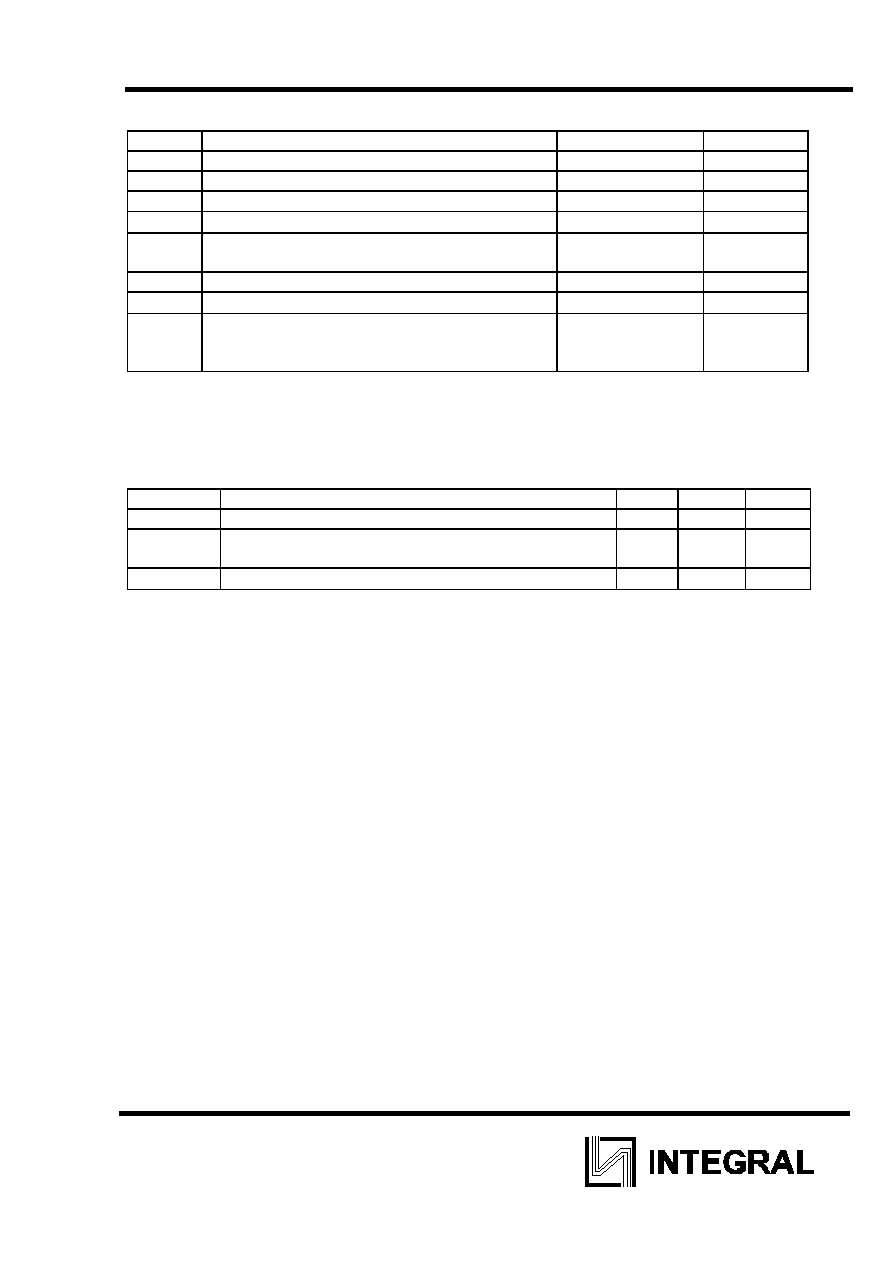
MAXIMUM RATINGS
*
Symbol Parameter
Value
Unit
V
CC
DC Supply Voltage (Referenced to GND)
-0.5 to +20
V
V
I
DC Input Voltage (Referenced to GND)
-0.5 to V
CC
+0.5
V
V
OUT
DC Output Voltage (Referenced to GND)
-0.5 to V
CC
+0.5
V
I
I
DC Input Current, per Pin
10
mA
P
D
Power Dissipation in Still Air, Plastic DIP+
SOIC Package+
750
500
mW
Ptot r Dissipation per Output Transistor
100
mW
Tstg
Storage Temperature
-65 to +150
�C
T
L
Lead Temperature, 1 mm from Case for 10
Seconds
(Plastic DIP or SOIC Package)
260
�C
*
Maximum Ratings are those values beyond which damage to the device may occur.
Functional operation should be restricted to the Recommended Operating Conditions.
+Derating - Plastic DIP: - 10 mW/
�C from 65� to 125�C
SOIC Package: : - 7 mW/
�C from 65� to 125�C
RECOMMENDED OPERATING CONDITIONS
Symbol Parameter Min
Max
Unit
V
CC
DC Supply Voltage (Referenced to GND)
3.0
18
V
V
I
, V
OUT
DC Input Voltage, Output Voltage (Referenced to
GND)
0 V
CC
V
T
A
Operating Temperature, All Package Types
-55
+125
�C
This device contains protection circuitry to guard against damage due to high static
voltages or electric fields. However, precautions must be taken to avoid applications of any voltage
higher than maximum rated voltages to this high-impedance circuit. For proper operation, V
IN
and
V
OUT
should be constrained to the range GND
�(V
IN
or V
OUT
)
�
VCC
.
Unused inputs must always be tied to an appropriate logic voltage level (e.g., either GND or
VCC
). Unused outputs must be left open.
IW4042B
3
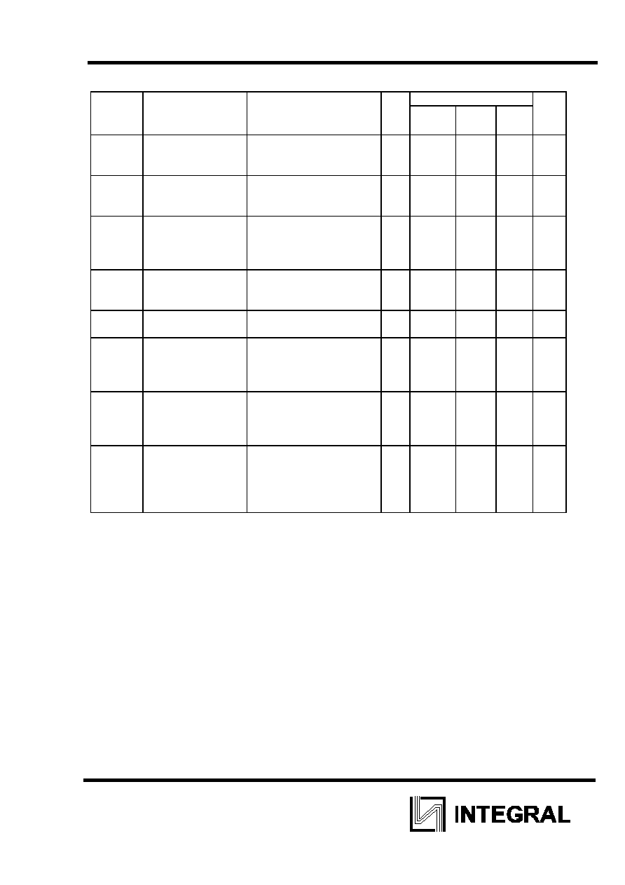
DC ELECTRICAL CHARACTERISTICS(Voltages Referenced to GND)
V
��
Guaranteed Limit
Symbol Parameter
Test
Conditions
V
�-55�C 25�C �125
�C
Unit
V
IH
Minimum
High-
Level Input
Voltage
V
OUT
=0.5 V or V
CC
- 0.5 V
V
OUT
=1.0 V or V
CC
- 1.0 V
V
OUT
=1.5 V or V
CC
- 1.5 V
5.0
10
15
3.5
7
11
3.5
7
11
3.5
7
11
V
V
IL
Maximum Low -
Level Input
Voltage
V
OUT
=0.5 V or V
CC
- 0.5 V
V
OUT
=1.0 V or V
CC
- 1.0 V
V
OUT
=1.5 V or V
CC
- 1.5 V
5.0
10
15
1.5
3
4
1.5
3
4
1.5
3
4
V
V
OH
Minimum
High-
Level Output
Voltage
V
IN
=GND or V
CC
5.0
10
15
4.95
9.95
14.95
4.95
9.95
14.95
4.95
9.95
14.9
5
V
V
OL
Maximum
Low-
Level Output
Voltage
V
IN
=GND or V
CC
5.0
10
15
0.05
0.05
0.05
0.05
0.05
0.05
0.05
0.05
0.05
V
I
IN
Maximum
Input
Leakage Current
V
IN
= GND or V
CC
18
0.1
0.1 1.0 A
I
��
Maximum
Quiescent Supply
Current
(per Package)
V
IN
= GND or V
CC
5.0
10
15
20
1
2
4
20
1
2
4
20
30
60
120
600
A
I
OL
Minimum
Output
Low (Sink)
Current
V
IN
= GND or V
CC
V
OL
=0.4 V
V
OL
=0.5 V
V
OL
=1.5 V
5.0
10
15
0.64
1.6
4.2
0.51
1.3
3.4
0.36
0.9
2.4
mA
I
OH
Minimum
Output
High (Source)
Current
V
IN
= GND or V
CC
V
OH
=2.5 V
V
OH
=4.6 V
V
OH
=9.5 V
V
OH
=13.5 V
5.0
5.0
10
15
-2.0
-0.64
-1.6
-4.2
-1.6
-0.51
-1.3
-3.4
-1.15
-0.36
-0.9
-2.4
mA
IW4042B
4
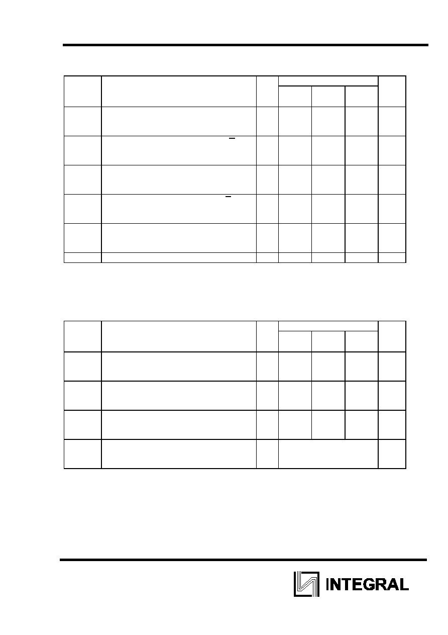
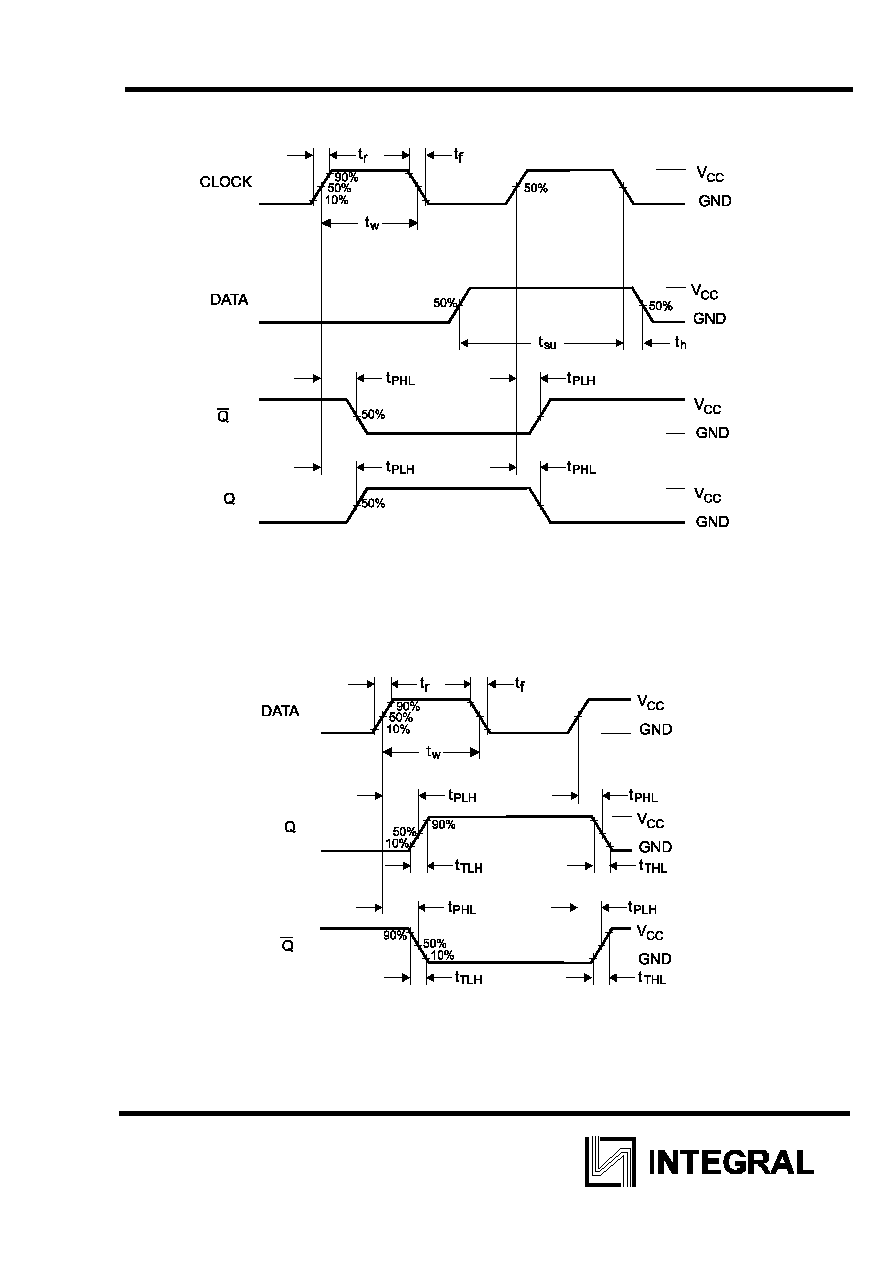
AC ELECTRICAL CHARACTERISTICS(C
L
=50pF, R
L
=200 k
, Input t
r
=t
f
=20 ns)
V
CC
Guaranteed Limit
Symbol Parameter V
�-55
�C
25
�C
�125
�C
Unit
t
PLH
,
t
PHL
Maximum Propagation Delay, Clock to
Q (Figure 1)
5.0
10
15
450
200
160
450
200
160
900
400
320
ns
t
PLH
,
t
PHL
Maximum Propagation Delay, Clock to
Q (Figure 1)
5.0
10
15
500
230
180
500
230
180
1000
460
360
ns
t
PLH
,
t
PHL
Maximum Propagation Delay, Data to Q
(Figure 2)
5.0
10
15
220
110
80
220
110
80
440
220
160
ns
t
PLH
,
t
PHL
Maximum Propagation Delay, Data to Q
(Figure 2)
5.0
10
15
300
150
100
300
150
100
600
300
200
ns
t
TLH
, t
THL
Maximum Output Transition Time, Any
Output (Figure 1)
5.0
10
15
200
100
80
200
100
80
400
200
160
ns
C
IN
Maximum Input Capacitance
-
7.5
pF
TIMING REQUIREMENTS(C
L
=50pF, R
L
=200 k
, Input t
r
=t
f
=20 ns)
V
CC
Guaranteed Limit
Symbol Parameter V
�-
55
�C
25
�C
�125�
C
Unit
t
w
Minimum Pulse Width, Clock (Figure 1)
5.0
10
15
200
100
60
200
100
60
400
200
120
ns
t
su
Minimum Setup Time, Data to Clock
(Figure 1)
5.0
10
15
50
30
25
50
30
25
100
60
50
ns
t
h
Minimum Hold Time, Clock to Data
(Figure 1)
5.0
10
15
120
60
50
120
60
50
240
120
100
ns
t
r
, t
f
Maximum Input Rise or Fall Time,
Clock (Figure 1)
5.0
10
15
Not rise or fall
time sensitive
s
IW4042B
5
Figure 1. Switching Waveforms
Figure 2. Switching Waveforms