 | –≠–ª–µ–∫—Ç—Ä–æ–Ω–Ω—ã–π –∫–æ–º–ø–æ–Ω–µ–Ω—Ç: IW4050BD | –°–∫–∞—á–∞—Ç—å:  PDF PDF  ZIP ZIP |
TECHNICAL DATA
93
Hex Buffer/Converter
High-Voltage Silicon-Gate CMOS
The IW4050B is noninverting hex buffers and feature logic-level
conversion using only one supply (voltage (V
CC
). The input-signal high
level (V
IH
) can exceed the V
CC
supply voltage when these devices are
used for logic-level conversions. These devices are intended for use as
CMOS to DTL/TTL converters.
û
Operating Voltage Range: 3.0 to 18 V
û
Maximum input current of 1
A at 18 V over full package-
temperature range; 100 nA at 18 V and 25
ú
C
û
Noise margin (over full package temperature range):
1.0 V min @ 5.0 V supply
2.0 V min @ 10.0 V supply
2.5 V min @ 15.0 V supply
û
High-to-low level conversion
IW4050B
ORDERING INFORMATION
IW4050BN Plastic
IW4050BD SOIC
T
A
= -55
ú
to 125
ú
C for all packages
LOGIC DIAGRAM
PINS 13, 16 = NO CONNECTION
PIN 1 =V
CC
PIN 8 = GND
PIN ASSIGNMENT
NC = NO CONNECTION
FUNCTION TABLE
Inputs
Output
A
Y
L
L
H
H

IW4050B
94
MAXIMUM RATINGS
*
Symbol
Parameter
Value
Unit
V
CC
DC Supply Voltage (Referenced to GND)
-0.5 to +20
V
V
IN
DC Input Voltage (Referenced to GND)
V
CC
**
to +18
V
V
OUT
DC Output Voltage (Referenced to GND)
-0.5 to V
CC
+0.5
V
I
IN
DC Input Current, per Pin
10
mA
P
D
Power Dissipation in Still Air, Plastic DIP+
SOIC Package+
750
500
mW
P
D
Power Dissipation per Output Transistor
100
mW
Tstg
Storage Temperature
-65 to +150
ú
C
T
L
Lead Temperature, 1 mm from Case for 10 Seconds
(Plastic DIP or SOIC Package)
260
ú
C
*
Maximum Ratings are those values beyond which damage to the device may occur.
Functional operation should be restricted to the Recommended Operating Conditions.
+Derating - Plastic DIP: - 10 mW/
ú
C from 65
ú
to 125
ú
C
SOIC Package: : - 7 mW/
ú
C from 65
ú
to 125
ú
C
**
The IW4050B has high-to-low level voltage conversion capability but not low-to-high level; therefore it is
recommended that V
IN
ô
V
CC
RECOMMENDED OPERATING CONDITIONS
Symbol
Parameter
Min
Max
Unit
V
CC
DC Supply Voltage (Referenced to GND)
3.0
18
V
V
IN
DC Input Voltage (Referenced to GND)
V
CC
**
18
V
V
OUT
DC Output Voltage (Referenced to GND)
0
V
CC
V
T
A
Operating Temperature, All Package Types
-55
+125
ú
C
**
The IW4050B has high-to-low level voltage conversion capability but not low-to-high level; therefore it is
recommended that V
IN
ô
V
CC
This device contains protection circuitry to guard against damage due to high static voltages or electric
fields. However, precautions must be taken to avoid applications of any voltage higher than maximum rated
voltages to this high-impedance circuit. For proper operation, V
IN
and V
OUT
should be constrained to the range
GND
ò
(V
IN
or V
OUT
)
ò
V
CC
.
Unused inputs must always be tied to an appropriate logic voltage level (e.g., either GND or V
CC
).
Unused outputs must be left open.
IW4050B
95
DC ELECTRICAL CHARACTERISTICS
(Voltages Referenced to GND)
V
CC
Guaranteed Limit
Symbol
Parameter
Test Conditions
V
ô
-55
ú
C
25
ú
C
ò
125
ú
C
Unit
V
IH
Minimum High-Level
Input Voltage
V
OUT
= V
CC
- 0.5V
V
OUT
= V
CC
- 1.0 V
V
OUT
= V
CC
- 1.5V
5.0
10
15
3.5
7
11
3.5
7
11
3.5
7
11
V
V
IL
Maximum Low -Level
Input Voltage
V
OUT
= 0.5V
V
OUT
= 1.0 V
V
OUT
= 1.5V
5.0
10
15
1.5
3
4
1.5
3
4
1.5
3
4
V
V
OH
Minimum High-Level
Output Voltage
V
IN
= V
CC
5.0
10
15
4.95
9.95
14.95
4.95
9.95
14.95
4.95
9.95
14.95
V
V
OL
Maximum Low-Level
Output Voltage
V
IN
=GND
5.0
10
15
0.05
0.05
0.05
0.05
0.05
0.05
0.05
0.05
0.05
V
I
IN
Maximum Input
Leakage Current
V
IN
= GND or V
CC
18
0.1
0.1
1.0
A
I
CC
Maximum Quiescent
Supply Current
(per Package)
V
IN
= GND or V
CC
5.0
10
15
20
1
2
4
20
1
2
4
20
30
60
120
600
A
I
OL
Minimum Output Low
(Sink) Current
V
IN
= GND or V
CC
U
OL
=0.4 V
U
OL
=0.4 V
U
OL
=0.5 V
U
OL
=1.5 V
4.5
5
10
15
3.3
4
10
26
2.6
3.2
8
24
1.8
2.4
5.6
18
mA
I
OH
Minimum Output
High (Source) Current
V
IN
= GND or V
CC
U
OH
=2.5 V
U
OH
=4.6 V
U
OH
=9.5 V
U
OH
=13.5 V
5.0
5.0
10
15
-2.6
-0.81
-2.0
-5.2
-2.1
-0.65
-1.65
-4.3
-1.55
-0.48
-1.18
-3.1
mA
IW4050B
96
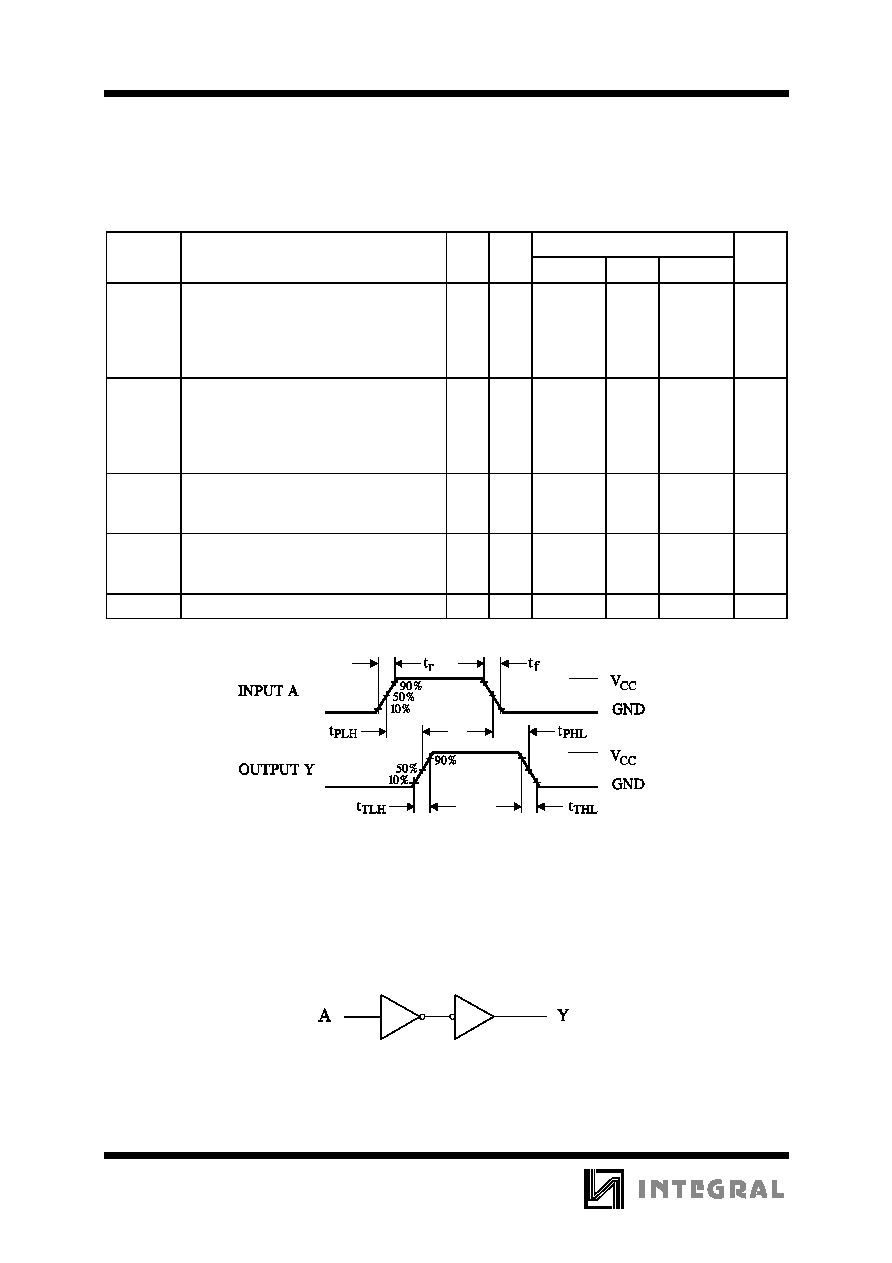
AC ELECTRICAL CHARACTERISTICS
(C
L
=50pF, R
L
=200k
, Input t
r
=t
f
=20 ns)
V
IN
V
CC
Guaranteed Limit
Symbol
Parameter
V
V
ô
-55
ú
C
25
ú
C
ò
125
ú
C
Unit
t
PLH
Maximum Propagation Delay, Input A to
Output Y (Figure 1)
5
10
10
15
15
5
10
5
15
5
140
80
90
60
80
140
80
90
60
80
280
160
180
120
160
ns
t
PHL
Maximum Propagation Delay, Input A to
Output Y (Figure 1)
5
10
10
15
15
5
10
5
15
5
110
55
100
30
100
110
55
100
30
100
220
110
200
60
200
ns
t
TLH
Maximum Output Transition Time, Any
Output (Figure 1)
5
10
15
5
10
15
160
80
60
160
80
60
320
160
120
ns
t
THL
Maximum Output Transition Time, Any
Output (Figure 1)
5
10
15
5
10
15
60
40
30
60
40
30
120
80
60
ns
C
IN
Maximum Input Capacitance
-
-
7.5
pF
Figure 1. Switching Waveforms
EXPANDED LOGIC DIAGRAM
(1/6 of the Device)