 | –≠–ª–µ–∫—Ç—Ä–æ–Ω–Ω—ã–π –∫–æ–º–ø–æ–Ω–µ–Ω—Ç: IW4060B | –°–∫–∞—á–∞—Ç—å:  PDF PDF  ZIP ZIP |

TECHNICAL DATA
115
14-Stage Ripple-Carry Binary
Counter/Divider and Oscillator
High-Voltage Silicon-Gate CMOS
The IW4060B consists of an oscillator section and 14 ripple-carry
binary counter stages. The oscillator configuration allows design of
either RC or crystal oscillator circuits. A RESET input is provided
which resets the counter to the all-Q's state and disables the oscillator.
A high level on the RESET line accomplishes the reset function. All
counter stages are master-slave flip-flops. The state of the counter is
advanced one step in binary order on the negative transition of OSC In
(and OSC Out). Schmitt trigger action on the input-pulse line permits
unlimited input-pulse rise and fall times.
û
Operating Voltage Range: 3.0 to 18 V
û
Maximum input current of 1
A at 18 V over full package-
temperature range; 100 nA at 18 V and 25
ú
C
û
Noise margin (over full package temperature range):
1.0 V min @ 5.0 V supply
2.0 V min @ 10.0 V supply
2.5 V min @ 15.0 V supply
IW4060B
ORDERING INFORMATION
IW4060BN Plastic
IW4060BD SOIC
T
A
= -55
ú
to 125
ú
C for all
packages
PIN ASSIGNMENT
FUNCTION TABLE
Inputs
Outputs
Osc In
Reset
Q
L
No change
L
Advance to
next state
X
H
All Outputs
are low
X = don't care
LOGIC DIAGRAM
PIN 16=V
CC
PIN 8= GND
IW4060B
116
MAXIMUM RATINGS
*
Symbol
Parameter
Value
Unit
V
CC
DC Supply Voltage (Referenced to GND)
-0.5 to +20
V
V
IN
DC Input Voltage (Referenced to GND)
-0.5 to V
CC
+0.5
V
V
OUT
DC Output Voltage (Referenced to GND)
-0.5 to V
CC
+0.5
V
I
IN
DC Input Current, per Pin
10
mA
P
D
Power Dissipation in Still Air, Plastic DIP+
SOIC Package+
750
500
mW
P
D
Power Dissipation per Output Transistor
100
mW
Tstg
Storage Temperature
-65 to +150
ú
C
T
L
Lead Temperature, 1 mm from Case for 10 Seconds
(Plastic DIP or SOIC Package)
260
ú
C
*
Maximum Ratings are those values beyond which damage to the device may occur.
Functional operation should be restricted to the Recommended Operating Conditions.
+Derating - Plastic DIP: - 10 mW/
ú
C from 65
ú
to 125
ú
C
SOIC Package: : - 7 mW/
ú
C from 65
ú
to 125
ú
C
RECOMMENDED OPERATING CONDITIONS
Symbol
Parameter
Min
Max
Unit
V
CC
DC Supply Voltage (Referenced to GND)
3.0
18
V
V
IN
, V
OUT
DC Input Voltage, Output Voltage (Referenced to GND)
0
V
CC
V
T
A
Operating Temperature, All Package Types
-55
+125
ú
C
This device contains protection circuitry to guard against damage due to high static voltages or electric
fields. However, precautions must be taken to avoid applications of any voltage higher than maximum rated
voltages to this high-impedance circuit. For proper operation, V
IN
and V
OUT
should be constrained to the range
GND
ò
(V
IN
or V
OUT
)
ò
V
CC
.
Unused inputs must always be tied to an appropriate logic voltage level (e.g., either GND or V
CC
).
Unused outputs must be left open.

IW4060B
117
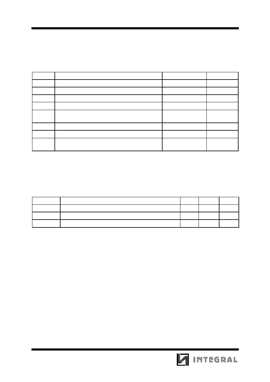
DC ELECTRICAL CHARACTERISTICS
(Voltages Referenced to GND)
V
CC
Guaranteed Limit
Symbol
Parameter
Test Conditions
V
ô
-55
ú
C
25
ú
C
ò
125
ú
C
Unit
V
IH
Minimum High-Level
Input Voltage
V
OUT
= 0.5 V or V
CC
- 0.5V
V
OUT
= 1.0 V or V
CC
- 1.0 V
V
OUT
= 1.5 V V
CC
- 1.5V
5.0
10
15
3.5
7
11
3.5
7
11
3.5
7
11
V
V
IL
Maximum Low -Level
Input Voltage
V
OUT
= 0.5 V or V
CC
- 0.5V
V
OUT
= 1.0 V or V
CC
- 1.0 V
V
OUT
= 1.5 V V
CC
- 1.5V
5.0
10
15
1.5
3
4
1.5
3
4
1.5
3
4
V
V
OH
Minimum High-Level
Output Voltage
V
IN
=GND or V
CC
5.0
10
15
4.95
9.95
14.95
4.95
9.95
14.95
4.95
9.95
14.95
V
V
OL
Maximum Low-Level
Output Voltage
V
IN
=GND or V
CC
5.0
10
15
0.05
0.05
0.05
0.05
0.05
0.05
0.05
0.05
0.05
V
I
IN
Maximum Input
Leakage Current
V
IN
= GND or V
CC
18
0.1
0.1
1.0
A
I
CC
Maximum Quiescent
Supply Current
(per Package)
V
IN
= GND or V
CC
5.0
10
15
20
5
10
20
100
5
10
20
100
150
300
600
3000
A
I
OL
Minimum Output Low
(Sink) Current
V
IN
= GND or V
CC
U
OL
=0.4 V
U
OL
=0.5 V
U
OL
=1.5 V
5.0
10
15
0.64
1.6
4.2
0.51
1.3
3.4
0.36
0.9
2.4
mA
I
OH
Minimum Output
High (Source) Current
V
IN
= GND or V
CC
U
OH
=2.5 V
U
OH
=4.6 V
U
OH
=9.5 V
U
OH
=13.5 V
5.0
5.0
10
15
-2
-0.64
-1.6
-4.2
-1.6
-0.51
-1.3
-3.4
-1.15
-0.36
-0.9
-2.4
mA

IW4060B
118
AC ELECTRICAL CHARACTERISTICS
(C
L
=50pF, R
L
=200k
, Input t
r
=t
f
=20 ns)
V
CC
Guaranteed Limit
Symbol
Parameter
V
ô
-55
ú
C
25
ú
C
ò
125
ú
C
Unit
f
max
Maximum Clock Frequency (50% Duty Cycle)
(Figure 1)
5.0
10
15
3.5
8
12
3.5
8
12
1.75
4
6
MHz
t
PHL
, t
PLH
Maximum Propagation Delay, Clock to Q4
(Figure 1)
5.0
10
15
740
300
200
740
300
200
1480
600
400
ns
t
PHL
, t
PLH
Maximum Propagation Delay, Q
n
to Q
n+1
(Figure 2)
5.0
10
15
200
100
80
200
100
80
400
200
160
ns
t
PHL
Maximum Propagation Delay, Reset to Any Q
(Figure 3)
5.0
10
15
360
160
100
360
160
100
720
320
200
ns
t
THL
, t
TLH
Maximum Output Transition Time, Any Output
(Figure 1)
5.0
10
15
200
100
80
200
100
80
400
200
160
ns
C
IN
Maximum Input Capacitance
-
7.5
pF
TIMING REQUIREMENTS
(C
L
=50pF, R
L
=200 k
, Input t
r
=t
f
=20 ns)
V
CC
Guaranteed Limit
Symbol
Parameter
V
ô
-55
ú
C
25
ú
C
ò
125
ú
C
Unit
t
w
Minimum Pulse Width, Clock (Figure 1)
5.0
10
15
100
40
30
100
40
30
200
80
60
ns
t
w
Minimum Pulse Width, Reset (Figure 3)
5.0
10
15
120
60
40
120
60
40
240
120
80
ns
t
f
, t
r
Maximum Input Rise and Fall Times (Figure 1)
5.0
10
15
Unlimited
ns

IW4060B
119
Figure 1. Switching Waveforms
Figure 2. Switching Waveforms
Figure 3. Switching Waveforms
EXPANDED LOGIC DIAGRAM
* R = HIGH DOMINATES (RESETS ALL STAGES)
** COUNTER ADVANCES ONE BINARY COUNT ON EACH NEGATIVE - GOING TRANSITION OF
CLOCK (AND OSC OUT)