TECHNICAL DATA
173
Programmable Timer
High-Performance Silicon-Gate CMOS
The IW4541 programmable timer consists of a 16-stage binary
counter, an oscillator that is controlled by external R-C components (2
resistors and a capacitor), an automatic power-on reset circuit, and
output control logic. The counter increments on positive-edge clock
transitons and can also be reset via the MASTER RESET input.
The output from this timer is the Q or not Q output from the 8th,
10th, 13th, or 16th counter stage. The desired stage is chosen using
time-select inputs A and B. The output is available in either of two
modes selectable via the MODE input, pin 10. When this MODE input
is a logic "1",the output will be a continuous square wave having a
frequency equal to the oscillator frequency divided by 2
N
. With the
MODE input set to logic "0" and after a MASTER RESET is initiated,
the output (assuming Q output has been selected) changes from a low
to a high state after 2
N-1
counts and remains in that state until another
MASTER RESET pulse is applied or the MODE input is set to a logic
"1".
Timing is initialized by setting the AUTO RESET input (pin 5) to logic "0"and turning power on. If pin 5 is
set to logic "1", the AUTO RESET circuit is disabled and counting will not start untill after a positive MASTER
RESET pulse is applied and returns to a low level. The AUTO RESET consumes an appreciable amount of
power and should not be used if low-power operation is desired. For reliable automatic power-on reset, V
CC
should be greater than 5V.
�
Operating Voltage Range: 3.0 to 18 V
�
Maximum input current of 1
A at 18 V over full package-temperature range; 100 nA at 18 V and 25
�
C
�
Noise margin (over full package temperature range):
1.0 V min @ 5.0 V supply
2.0 V min @ 10.0 V supply
2.5 V min @ 15.0 V supply
IW4541B
ORDERING INFORMATION
IW4541BN Plastic
IW4541BD SOIC
T
A
= -55
�
to 125
�
C for all packages
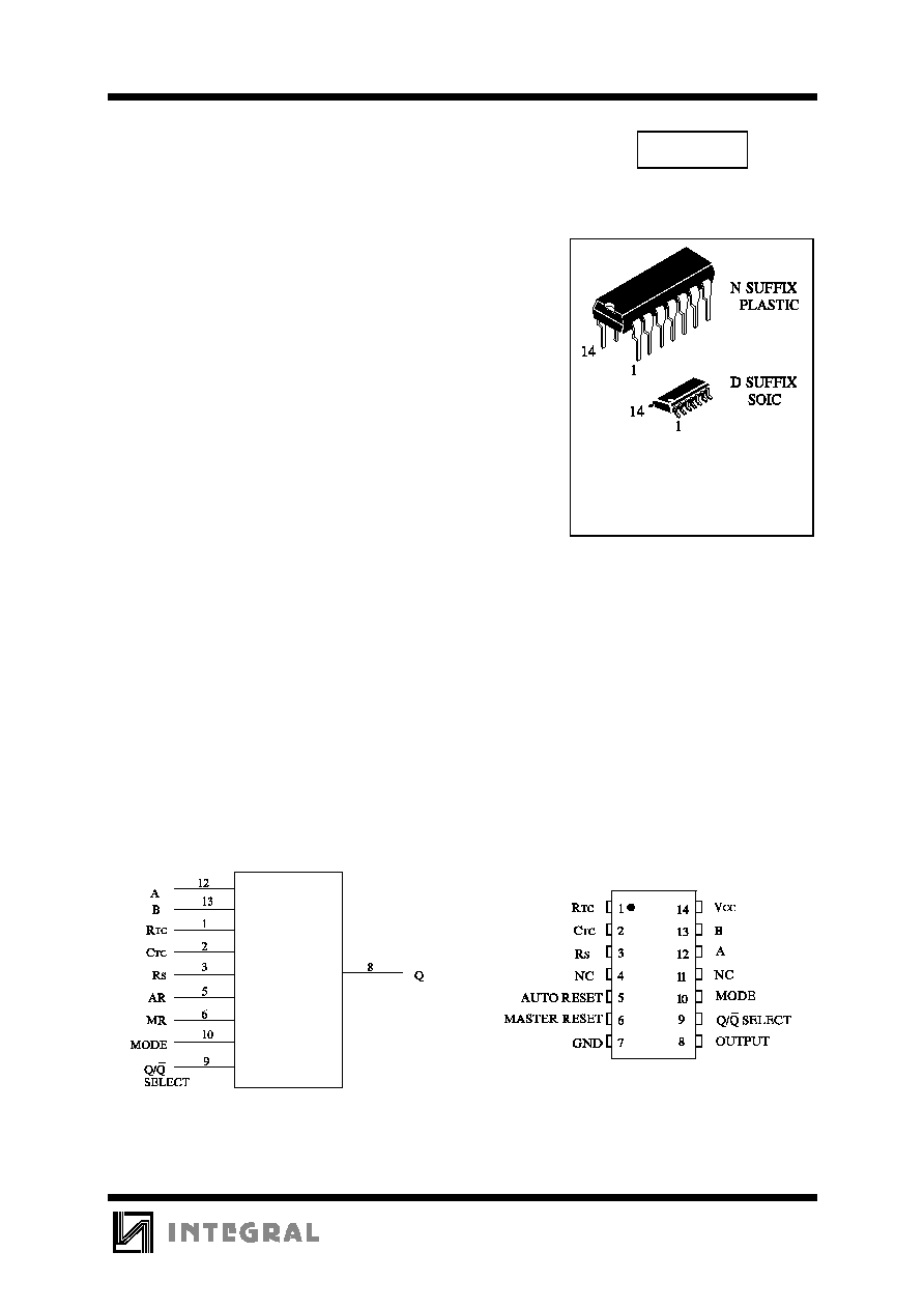
LOGIC DIAGRAM
PIN 14 =V
CC
PIN 7 = GND
PINS 4,11 = NO CONNECTION
PIN ASSIGNMENT
NC = NO CONNECTION

IW4541B
174
MAXIMUM RATINGS
*
Symbol
Parameter
Value
Unit
V
CC
DC Supply Voltage (Referenced to GND)
-0.5 to +20
V
V
IN
DC Input Voltage (Referenced to GND)
-0.5 to V
CC
+0.5
V
V
OUT
DC Output Voltage (Referenced to GND)
-0.5 to V
CC
+0.5
V
I
IN
DC Input Current, per Pin
10
mA
P
D
Power Dissipation in Still Air, Plastic DIP+
SOIC Package+
750
500
mW
P
D
Power Dissipation per Output Transistor
100
mW
Tstg
Storage Temperature
-65 to +150
�
C
T
L
Lead Temperature, 1 mm from Case for 10 Seconds
(Plastic DIP or SOIC Package)
260
�
C
*
Maximum Ratings are those values beyond which damage to the device may occur.
Functional operation should be restricted to the Recommended Operating Conditions.
+Derating - Plastic DIP: - 10 mW/
�
C from 65
�
to 125
�
C
SOIC Package: : - 7 mW/
�
C from 65
�
to 125
�
C
RECOMMENDED OPERATING CONDITIONS
Symbol
Parameter
Min
Max
Unit
V
CC
DC Supply Voltage (Referenced to GND)
3.0
18
V
V
IN
, V
OUT
DC Input Voltage, Output Voltage (Referenced to GND)
0
V
CC
V
T
A
Operating Temperature, All Package Types
-55
+125
�
C
This device contains protection circuitry to guard against damage due to high static voltages or electric
fields. However, precautions must be taken to avoid applications of any voltage higher than maximum rated
voltages to this high-impedance circuit. For proper operation, V
IN
and V
OUT
should be constrained to the range
GND
�
(V
IN
or V
OUT
)
�
V
CC
.
Unused inputs must always be tied to an appropriate logic voltage level (e.g., either GND or V
CC
).
Unused outputs must be left open.

IW4541B
175
DC ELECTRICAL CHARACTERISTICS
Digital Section
V
CC
Guaranteed Limit
Symbol
Parameter
Test Conditions
V
�
-55
�
C
�
25
�
C
�
125
�
C
Unit
V
IH
Minimum High-Level
Input Voltage
V
OUT
=0.5V or V
CC
-0.5V
V
OUT
=1.0V or V
CC
-1.0V
V
OUT
=1.5V or V
CC
-1.5V
5
10
15
3.5
7
11
3.5
7
11
3.5
7
11
V
V
IL
Maximum Low -Level
Input Voltage
V
OUT
=0.5V or V
CC
-0.5V
V
OUT
=1.0V or V
CC
-1.0V
V
OUT
=1.5V or V
CC
-1.5V
5
10
15
1.5
3
4
1.5
3
4
1.5
3
4
V
V
OH
Minimum High-Level
Output Voltage
V
IN
=GND or V
CC
5.0
10
15
4.95
9.95
14.95
4.95
9.95
14.95
4.95
9.95
14.95
V
V
OL
Maximum Low-Level
Output Voltage
V
IN
=GND or V
CC
5.0
10
15
0.05
0.05
0.05
0.05
0.05
0.05
0.05
0.05
0.05
V
I
IN
Maximum Input
Leakage Current
V
IN
= GND or V
CC
18
0.1
0.1
1.0
A
I
CC
Maximum Quiescent
Supply Current
(per Package)
V
IN
= GND or V
CC
5.0
10
15
20
5
10
20
100
5
10
20
100
150
300
600
3000
A
I
OL
Minimum Output Low
(Sink) Current
V
IN
= GND or V
CC
U
OL
=0.4 V
U
OL
=0.5 V
U
OL
=1.5 V
5.0
10
15
1.9
5
12.6
1.55
4
10
1.08
2.8
7.2
mA
I
OH
Minimum Output High
(Source) Current
V
IN
= GND or V
CC
U
OH
=2.5 V
U
OH
=4.6 V
U
OH
=9.5 V
U
OH
=13.5 V
5.0
5.0
10
15
-6.2
-1.9
-5
-12.6
-5
-1.55
-4
-10
-3
-1.08
-2.8
-7.2
mA

IW4541B
176
AC ELECTRICAL CHARACTERISTICS
(C
L
=50pF, R
L
=200k
, Input t
r
=t
f
=20 ns)
V
CC
Guaranteed Limit
Symbol
Parameter
V
�
-55
�
C
25
�
C
�
125
�
C
Unit
f
max
Maximum Clock Frequency (Figure 1)
5.0
10
15
1.5
4
6
1.5
4
6
0.75
2
3
MHz
t
PLH
, t
PHL
Maximum Propagation Delay,
Clock to Q (Figure 1)
(2
8
)
5.0
10
15
10.5
3.8
2.9
10.5
3.8
2.9
21
7.6
5.8
ns
(2
16
)
5.0
10
15
18
10
7.5
18
10
7.5
36
20
15
t
THL
Maximum Output Transition Time, Any Output
(Figure 1)
5.0
10
15
200
100
80
200
100
80
400
200
160
ns
t
TLH
Maximum Output Transition Time, Any Output
(Figure 1)
5.0
10
15
360
180
130
360
180
130
720
360
260
C
IN
Maximum Input Capacitance
-
7.5
pF
TIMING REQUIREMENTS
(C
L
=50pF, R
L
=200k
, Input t
r
=t
f
=20 ns)
V
CC
Guaranteed Limit
Symbol
Parameter
+25
�
C
-40
�
C
to +85
�
C
Unit
t
w
Minimum Pulse Width, Master Reset or Clock
(Figure 1)
5
10
15
900
300
225
1800
600
450
ns
t
r
,t
f
Maximum Rise and Fall Time, Clock
(Figure 1)
5
10
15
Unlimited
s

IW4541B
177
Figure 1. Switching Weveforms
EXPANDED LOGIC DIAGRAM
FREQUENCY SELECTION TABLE
INPUTS
No. of Stages
Count
A
B
N
2
N
L
L
13
8192
L
H
10
1024
H
L
8
256
H
H
16
65536
FUNCTION TABLE
PIN
STATE
0
1
5
Auto Reset On
Auto Reset Disable
6
Master Reset Off
Master Reset On
9
Output Initially
Low After Reset
(Q)
Output Initially High
After Reset (not Q)
10
Single Transition
Mode
Recycle Mode