
IZ1236
1
8-
DIGIT
C
ALCULATOR WITH MARKER
The IZ1236ÃR is a single chip CMOS LSI with 8-digitt arithmetic operation, with marker,
LCD control, and auto power off function, designed for FEM LCD operation with a 1.5V
power supply.
FUNCTIONS:
- basic arithmetical operations over eight-digit numbers;
- operations with memory;
- percentage calculation;
- square root calculation;
- calculation of reverse value of number;
- operations with constants;
- indication of additional operations.
Microcircuit.
ABSOLUTE MAXIMUM RATINGS
Symbol
Name of parameter
Extreme mode
Limiting mode
Unit
min
max
min
max
U
DD
Supply
voltage
1.1
1.8
-0.3 2.1
V
U
SB
Supply voltage from solar
battery
1.1 3.0 -0.3
3.3 V
U
IH
input voltage of high level
U
DD
-0.4 U
DD
-
U
DD
+0.3 V
U
IL
Input voltage of low level
0
0.4
-0.3
-
V
“amb
Operating temperature range
0
55
-
-
ú
—
“stg Storage
temperature
-
-
-60 125
ú
—
IZ1236
2
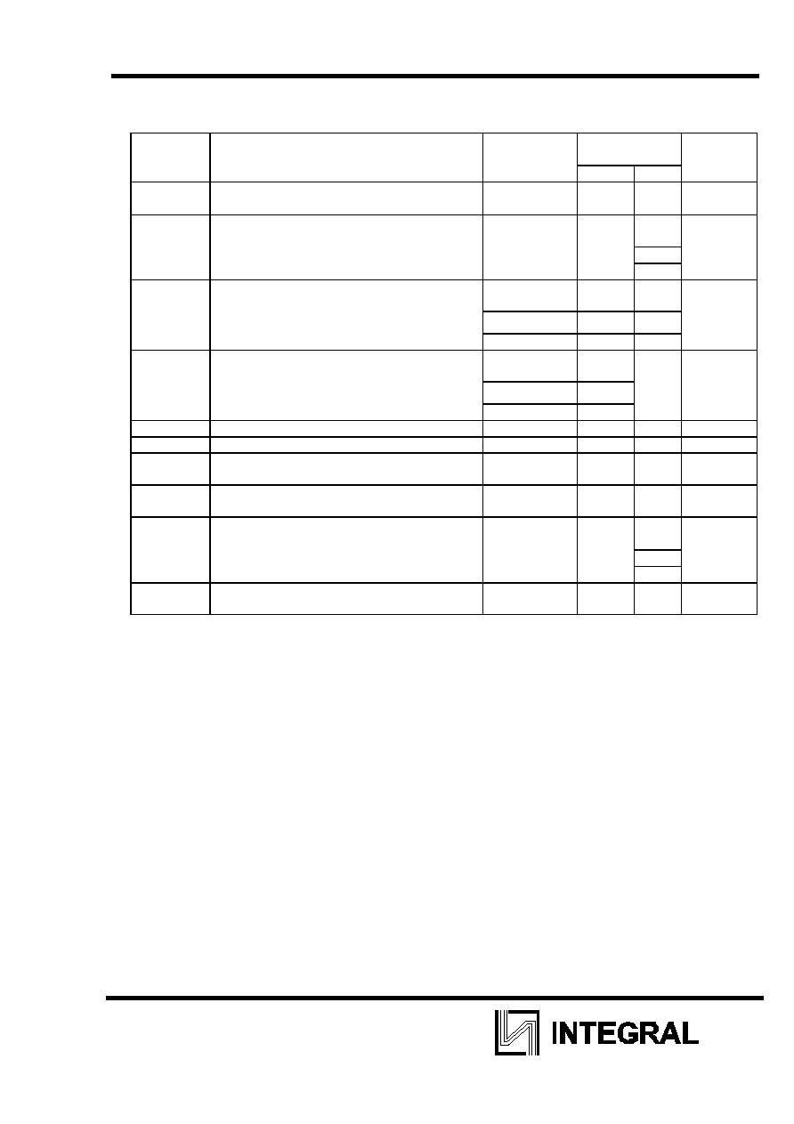
ELECTRICAL CHARACTERISTICS (T
a
= 25
o
C, V
DD
= +3.0V
0.2V, V
SS
=0V )
Symbol
Name of the parameter
Mode of
measurement
Standard Unit
min
max
U
OL
Output voltage of low level on outputs P1,
P2, A2-A5
U
DD
=1.5 V
I
OL
=15
¿
- 0.15 V
U
OL1
Output voltage of low level on outputs ý1-ý8,
‚1-‚8, Ò1-Ò8, Õ1-Õ3
U
DD
=1.1 V
-
0.2
V
U
DD
=1.5 V
0.2
U
DD
=1.8 V
0.2
U
OH1
Output voltage of high level on outputs Õ1-
Õ3
U
DD
=1.1 V
0.9
1.3
V
U
DD
=1.5 V
1.3
1.7
U
DD
=1.8 V
1.6
2.0
U
OH2
Output voltage of high level on outputs ý1-
ý8, ‚1-‚8, Ò1-Ò8, Õ1-Õ3
U
DD
=1.1 V
2.0
-
V
U
DD
=1.5 V
2.8
U
DD
=1.8 V
3.4
U
C
Voltage on voltage doubler
U
DD
=1.1 V
2.0
-
V
U
ST
Voltage on stabilizer of solar battery
U
I
=3.0 V
1.6
2.0
V
I
IL
Input current of low level on inputs K2-K6
U
DD
=1.5 V
U
IL
=0 V
0.3 3.0
¿
I
IH
Input current of high level on inputs K2-K6
U
DD
=1.8 V
U
IH
=1.8 V
- 1.0
¿
Idis
Consumption current, in mode :
- "disoperation";
U
DD
=1.3 V
-
5.0
¿
Iopr
- "in operation ";
U
DD
=1.1 V
7.0
Ioff
- " switched off"
U
DD
=1.5 V
0.1
Td
Period of displaying information on LCD
U
DD
=1.3 V
-
18
mÒ

IZ1236
3
PURPOSE OF CONTACT PADS
Number of
contact pad
Symbol Purpose
01 U
SB
Input of solar battery stabilizer
02
4
Keyboard control input
03
6
Keyboard control input
04
5
Keyboard control input
05
–1
Keyboard strobe output
06
–2
Keyboard strobe output
07
¿5
Keyboard strobe output
08
¿4
Keyboard strobe output
09
¿3
Keyboard strobe output
10
¿2
Keyboard strobe output
11
2
Keyboard control input
12
3
Keyboard control input
13
TST
Test input
14
VB
Pin for capacity connection
15
VA
Pin for capacity connection
16
VC
Pin for capacity connection
17
GND
General output
18
H3
LCD general electrode control output
19
H2
LCD general electrode control output
20
c8
LCD segment control output
21
b8
LCD segment control output
22
a8
LCD segment control output
23
c7
LCD segment control output
24
b7
LCD segment control output
25
a7
LCD segment control output
26
c6
LCD segment control output
27
b6
LCD segment control output
28
a6
LCD segment control output
29
c5
LCD segment control output
30
b5
LCD segment control output
31
a5
LCD segment control output
32
c4
LCD segment control output
33
b4
LCD segment control output
34
a4
LCD segment control output
35
c3
LCD segment control output
36
b3
LCD segment control output
37
a3
LCD segment control output
38
c2
LCD segment control output
39
b2
LCD segment control output
40
a2
LCD segment control output
41
c1
LCD segment control output
42
b1
LCD segment control output
43
a1
LCD segment control output
44
H1
LCD general electrode control output
45 U
DD
Power pin from voltage source
46 U
OP
Solar battery stabilizer output
Note - LCD -liquid crystal display

