 | –≠–ª–µ–∫—Ç—Ä–æ–Ω–Ω—ã–π –∫–æ–º–ø–æ–Ω–µ–Ω—Ç: IZ74LV620 | –°–∫–∞—á–∞—Ç—å:  PDF PDF  ZIP ZIP |
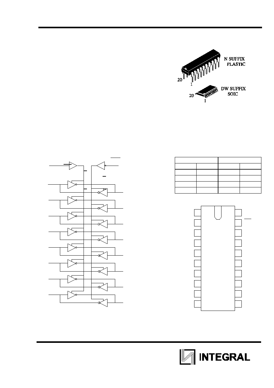
IN74LV620
1
O
CTAL
3-S
TATE
I
NVERTING
B
US
T
RANSCEIVER
Microcircuits IN74LV620 are pin-to-pin compatible with
microcircuits of series 74ALS620, 74HC620, 74HCT620.
Input voltage levels are compatible with standard C-MOS
levels
Features:
Output voltage levels are compatible with input levels C-
MOS, N-MOS and TTL microcircuits.
Supply voltage range from 1.2 to 3.6 V.
Maximum input current: 1.0 mkA; 0.1 mkA at “ = 25
ú—.
Consumption current 8 mA.
ORDERING INFORMATION
IN74LV620N
Plastic
IN74LV620D
SOIC
IZ74LV620
Chip
T
A
= -40
ú ü 125ú C for all packages
Truth table
Inputs Inputs/Outputs
OEB OEA ¿
¬
L L
A=B
input
H H
input
B=A
L H Z Z
H H
A=B
B=A
Block diagram
18
B
8
03
17
B
1
A
1
04
16
B
2
A
2
05
15
B
3
A
3
06
14
B
4
A
4
07
13
B
5
A
5
08
12
B
6
A
6
09
11
B
7
A
7
01
OEB
02
19
OEA
A
8
Pinout
620
OEB
01
A
8
02
A
1
03
A
2
04
A
3
05
A
4
06
A
5
07
A
6
08
A
7
09
GND
10
20
19
18
17
16
15
14
13
12
11
B
8
B
1
B
2
B
3
B
4
B
5
B
6
B
7
OEA
V
CC
IN74LV620
2
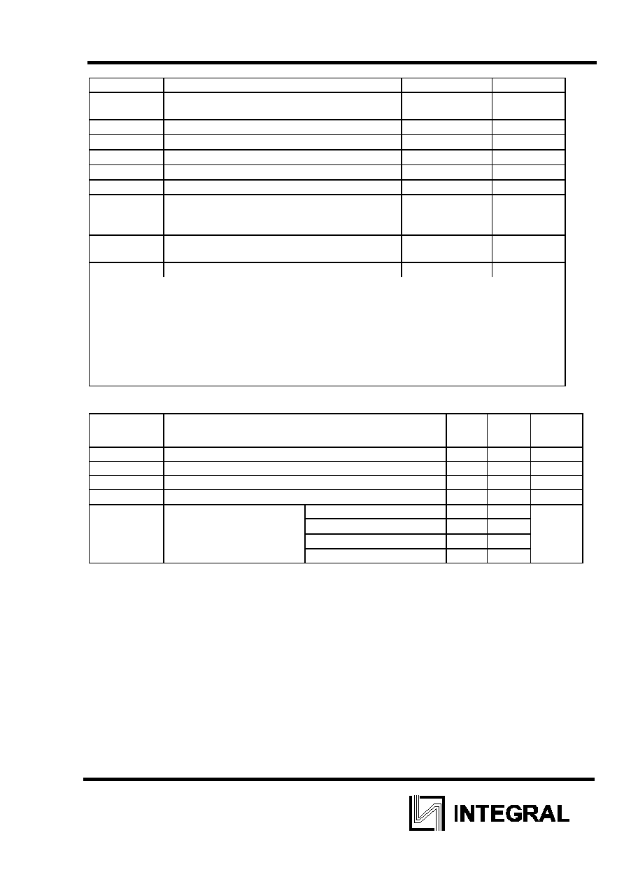
Absolute maximum ratings*
Symbol Parameter
Value
Unit
V
CC
Supply voltage
from -0.5 to
+5.0
V
I
IK
*
1
Input diode current
20
mA
I
OK
*
2
Output diode current
50
mA
I
O
*
3
Output current source-drain
35
mA
I
CC
Supply output current
70
mA
I
GND
Common output current
70
mA
P
D
Dissipation power at free air change,
Plastic
DIP
*
4
SOIC *
4
750
500
mW
Tstg
Storage temperature
from -65 to
+150
úC
T
L
260
úC
*
Under absolute maximum conditions operation of microcircuits is not guaranteed.
Operation under maximum conditions is guaranteed.
*
1
If V
I
< -0.5V or V
I
> V
CC
+ 0.5 V.
*
2
If V
O
< -0.5V or V
O
> V
CC
+ 0.5 V.
*
3
If -0.5V < V
O
< V
CC
+ 0.5 V.
*
4
Under operation in the temperature range from 65
ú— to 125úC value of dissipation power
drops down - to 10 mW/
úC for Plastic DIP
- to 7 mW/
úC for SOIC
Maximum conditions
Symbol Parameter Min
Max
Unit
V
CC
Supply
voltage
1.2
3.6 V
V
IN
Input
voltage
0 V
CC
V
V
OUT
Output
voltage
0 V
CC
V
T
A
Operation temperature. For all packages
-40
125
úC
V
CC
=1.2 ¬ 0
1000
V
CC
=2.0 ¬
700
V
CC
=3.0 ¬
500
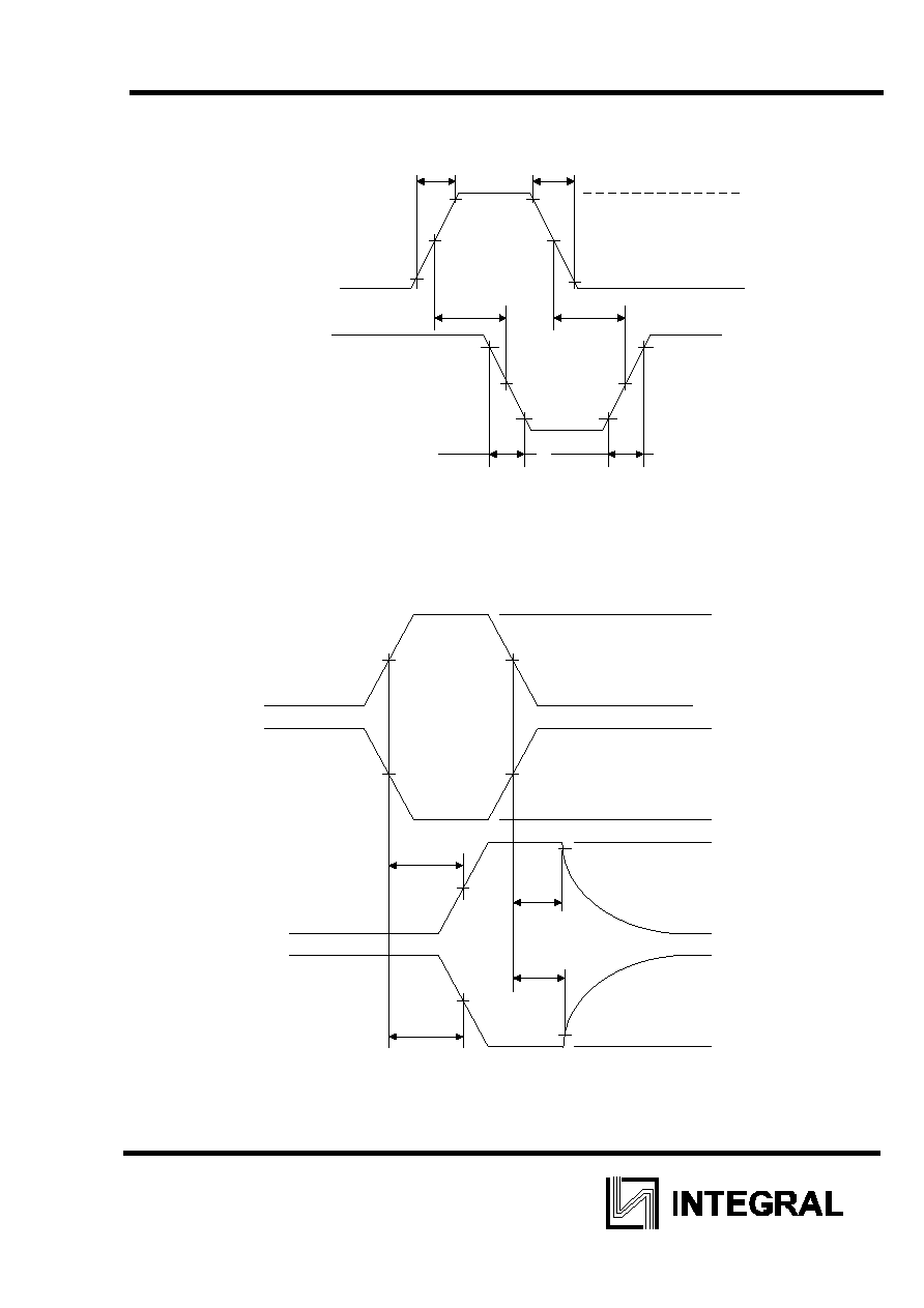
t
LH
, t
HL
Period of signal rise and
fall edges (Figure 1)
V
CC
=3.6 ¬
400
ns
IN74LV620
3
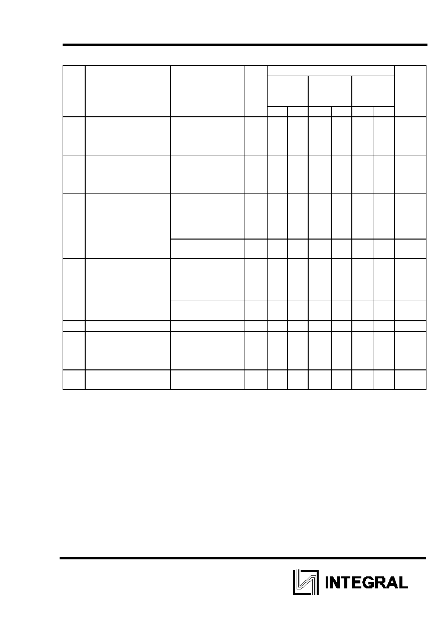
DC electrical characteristics
Value
25
úC
From -
40
úC to
85
úC
From -
40
úC to
125
úC
Sym
bol
Parameter Test
conditions
V
CC
,
V
min max min max min max
Unit
V
IH
High input voltage
V
O
= V
CC
-0.1 V
1.2
2.0
3.0
3.6
0.9
1.4
2.1
2.5
-
-
-
-
0.9
1.4
2.1
2.5
-
-
-
-
0.9
1.4
2.1
2.5
-
-
-
-
V
V
IL
Low input voltage
V
O
=0.1 V
1.2
2.0
3.0
3.6
-
-
-
-
0.3
0.6
0.9
1.1
-
-
-
-
0.3
0.6
0.9
1.1
-
-
-
-
0.3
0.6
0.9
1.1
V
V
OH
High output voltage
V
I
= V
IH
or V
IL
Io = -50 mkA
1.2
2.0
3.0
3.6
1.11
1.91
2.91
3.51
-
-
-
-
1.1
1.9
2.9
3.5
-
-
-
-
1.1
1.9
2.9
3.5
-
-
-
-
V
V
I
= V
IH
or V
IL
Io = -8 mA
3.0 2.48
- 2.34 - 2.20
-
V
V
OL
Low output voltage
V
I
= V
IH
or V
IL
Io = 50 mkA
1.2
2.0
3.0
3.6
-
-
-
-
0.09
0.09
0.09
0.09
-
-
-
-
0.1
0.1
0.1
0.1
-
-
-
-
0.1
0.1
0.1
0.1
V
V
I
= V
IH
or V
IL
Io = 8 mA
3.0 - 0.33
- 0.4 - 0.5 V
I
I
Input
current
V
I
= V
CC
or 0 V
3.6
-
0.1
-
1.0 - 1.0
uA
I
OZ
Output current in off
state
Outputs in the third
state
V
I
= V
IL
or V
IH
V
O
=V
CC
or 0 V
3.6 -
0.5
-
5
-
10
uA
I
CC
Consumption
current V
I
=V
CC
or 0 V
Io = 0 mkA
3.6 - 8.0
- 80 - 160
uA
IN74LV620
4
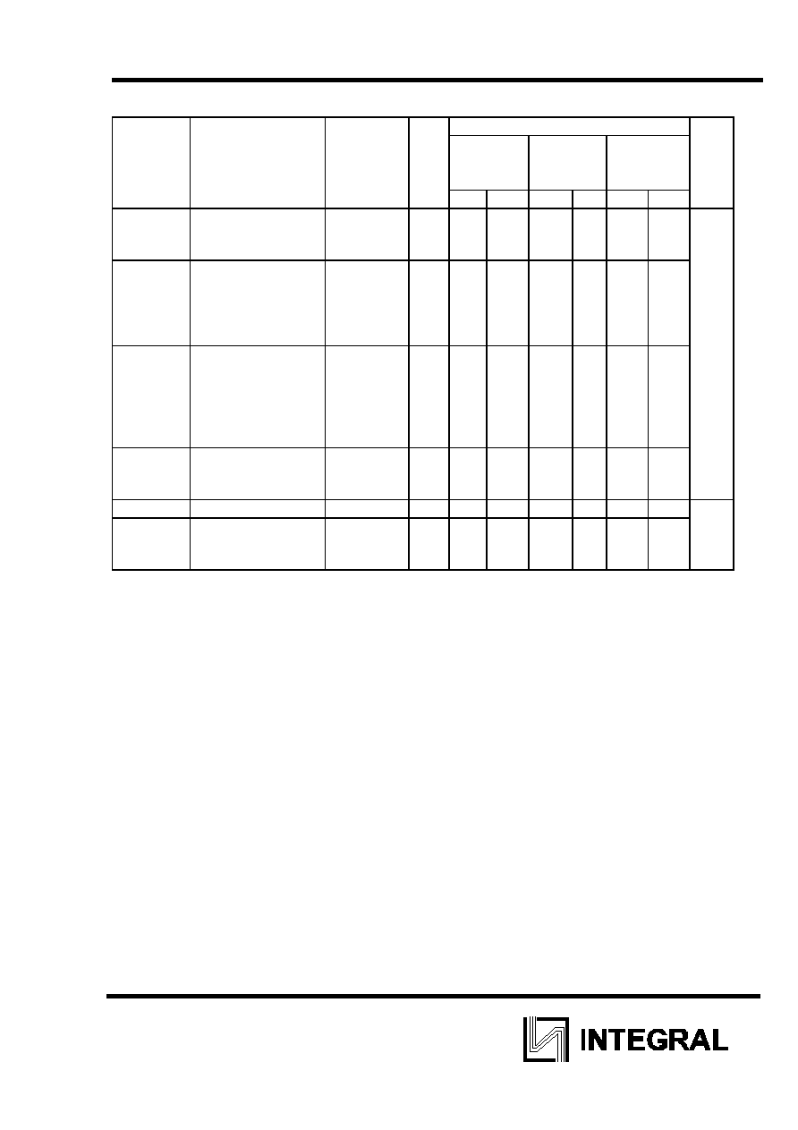
AC electrical characteristics (C
L
=50 pF, t
LH
= t
HL
= 6.0 ns)
Value
25
úC
From -
40
úC to
85
úC
From -40
úC
to 125
úC
Sym-bol Parameter Test
conditions
V
CC
,
V
min max min max min max
Unit
t
PHL,
t
PLH
from A to B
from B to A
Propagation delay
time in on and
off states
Fig.1 1.2
2.0
3.0
-
-
-
100
23
14
-
-
-
125
28
18
-
-
-
140
34
21
ns
t
PHZ
t
PLZ
from OE to
Y
Propagation delay
time when
switching from high,
low levels into off
state
Fig.2 1.2
2.0
3.0
-
-
-
120
30
20
-
-
-
140
37
24
-
-
-
160
43
28
t
PZH
t
PZL
from OE to
Y
Propagation delay
time when
switching from
off state into
high, low levels
Fig.2 1.2
2.0
3.0
-
-
-
120
28
17
-
-
-
140
35
21
-
-
-
160
43
26
t
THL,
t
TLH
Transition
time
when switching on,
off
Fig.1 1.2
2.0
3.0
-
-
-
60
16
10
-
-
-
75
20
13
-
-
-
90
24
15
C
I
Input
capacitance
3.0 -
7 - - - - pF
C
PD
Dynamic
capacitance (for
one channel)
V
I
= 0 V or
V
CC
3.0
-
50 - - - -
IN74LV620
5
- Time diagram of control of AC characteristics t
PLH
, t
PHL
0.9
0.1
0.9
0.1
t
LH
t
HL
t
PH
L
t
PL
H
V
CC
GND
A, B
B, A
V
CC
V
I
t
THL
t
TLH
0.9
0.9
0.1
0.1
V
I
= 0.5V
CC
V
I
V
I
V
I
Fig.1
- Time diagram of control of AC characteristics t
PLZ
, t
PHZ
, t
PZL
, t
PZH
V
CC
GND
OEA
0.9
0.1
t
PZH
t
PZL
t
PHZ
t
PLZ
A, B
A, B
V
OH
0 V
V
CC
V
OL
V
I
0.1
V
CC
GND
OEB
V
I
V
I
V
I
V
I
V
I
V
I
= 0.5V
CC
Fig.2