 | –≠–ª–µ–∫—Ç—Ä–æ–Ω–Ω—ã–π –∫–æ–º–ø–æ–Ω–µ–Ω—Ç: IZD1520U | –°–∫–∞—á–∞—Ç—å:  PDF PDF  ZIP ZIP |
IZD1520U
1
DOT MATRIX LIQUID CRYSTAL DISPLAY CONTROLLER &
DRIVER
FEATURES
û CMOS LSI chips
û Connection with CPU
Can be directly coupled with 80-port or 68-port system
û Available in chip form or in 100-pin plastic QFP
û Pin-to-Pin Replacement for SED1520 Series
û Many command set
û Total 80 (segment+common) drive sets
û Low power consumption - 30W maximum at 2kHz
external clock
û Power supply V
DD
- V
SS
: 2.4 to -7.0V
V
DD
- V
5
: 3.5 to -13.0V
DESCRIPTION
The IZD1520 family of dot matrix LCD (Liquid Crystal Display) drivers are designed for the
display of characters and graphics.
The drivers generate LCD drive signals derived from bit mapped data stored in an internal
RAM.
The IZD1520 family drivers incorporate innovative circuit design strategies to achieve very
low power dissipation at a wide range of operating voltages.
These features give the designer a flexible means of implementing small to medium size
LCD displays for compact, low power systems.
The IZD1520 which is able to drive two lines of twelve characters each.
The IZD1521 which is able to drive 80 segments for extention.
ABSOLUTE MAXIMUM RATINGS
Characteristic Symbol
Value
Unit
Supply Voltage (1)
V
SS
- 8.0 ~ 0.3
V
Supply Voltage (2)
V
5
- 16.5 ~ 0.3
V
Supply Voltage (3)
V
1,
V
2,
V
3,
V
4
V
5
~ 0.3
V
Input Voltage
V
I
V
SS
- 0.3 ~ 0.3
V
Output Voltage
V
O
V
SS
- 0.3 ~ 0.3
V
Power Dissipation
P
D
250
mW
Operating Temperature
T
a
- 10 ~ + 75
o
C
Storage Temperature
T
stg
- 65 ~ + 150
o
C
Soldering temperature time (10 sec
max)
T
sol
260
o
C
Notes:
1.
All voltages are specified relative to V
DD
= 0V.
2.
The following relation must be always hold
V
DD
ô V
1
ô V
2
ô V
3
ô V
4
ôV
5
.
3.
Exceeding the absolute maximum ratings may cause permanent damage to
the device. Functional operating under these
conditions is not implied.
IZD1520U
2
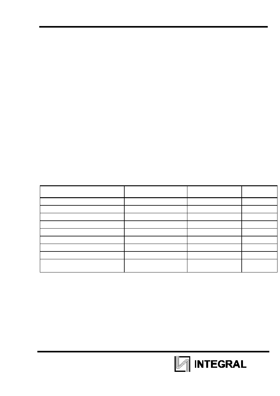
LINE-UP
Clock Frequency
Product
Name
On-chip External
Applicable Driver
Number of
SEGMENT
Drivers
Number of
COMMON
Drivers
Duty
IZD1520
OA
18kHz 18kHz IZ1520
OA
, IZ1521
OA
61 16
1/16,
1/32
IZD1521
OA
- 18kHz
IZ1520
OA
80
0
1/8 ~ 1/32
IZD1520
AA
- 2kHz
IZ1520
AA
, IZ1521
AA
61 16
1/16,
1/32
IZD1521
AA
- 2kHz
IZ1520
AA
80
0
1/8 ~ 1/32
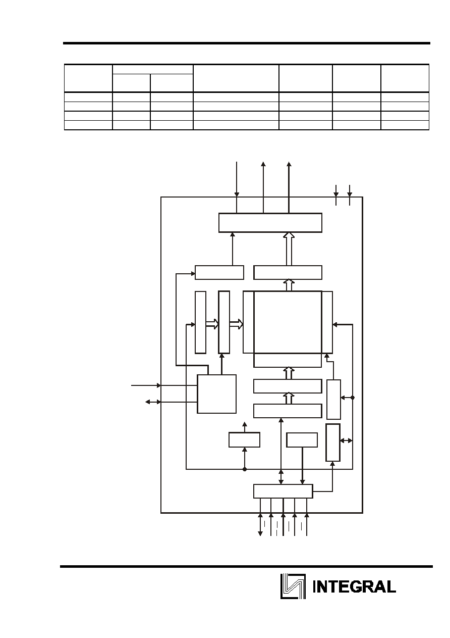
BLOCK DIAGRAM IZ1520AA
Display data RAM
(2560-bit)
Display data latch circuit
Common counter
LCD drive circuit
Column address decoder
Column address counter
Column address register
Status
Command
decoder
Display
timing
generator
circuit
L
o
w
-
a
ddr
ess
re
g
i
s
t
er
Bus
ho
l
d
e
r
MPU interface
D-
D
07
A0
,
C
S
RD
,RW
(E
,
R
W
)
M/
S
RE
S
CL
FR
Lin
e
addr
ess
de
c
o
de
r
Li
ne
c
o
u
n
t
e
r
D
i
spl
a
y
star
t lin
e
regis
t
e
r
I
/
O
bu
ffe
r
V
DD
V
SS
SE
G
t
o
S
E
G
06
0
CO
M
to
CO
M
01
5
V,
V,
V,
V,
V
1
2345
BLOCK DIAGRAM IZD1520
OA
IZD1520U
3
Display data RAM
(2560-bit)
Display data latch circuit
Common counter
LCD drive circuit
Column address decoder
Column address counter
Column address register
Status
Command
decoder
Display
timing
generator
circuit
L
o
w
-
ad
dr
e
s
s
reg
i
s
t
er
Bus
ho
l
d
e
r
MPU interface
D-
D
07
OS
C1
RD
,RW
(E
,
R
W
)
M/
S
RE
S
OSC2
FR
Lin
e
ad
dr
e
ss d
e
c
o
de
r
Lin
e
c
o
u
n
t
e
r
D
i
spl
a
y
star
t lin
e
r
e
giste
r
I
/
O
bu
ffe
r
V
DD
V
SS
SE
G
t
o
S
E
G
06
0
CO
M
to
CO
M
01
5
V
,
V,
V,
V,
V
1
2
345
IZD1520U
4
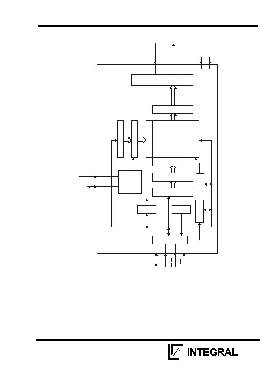
BLOCK DIAGRAM IZD1521
AA,
IZD1521
OA
Display data RAM
(2560-bit)
Display data latch circuit
LCD drive circuit
Column address decoder
Column address counter
Column address register
Status
Command
decoder
Display
timing
generator
circuit
Lo
w
-
a
d
d
r
e
s
s
re
g
i
s
t
e
r
Bu
s
ho
l
d
e
r
MPU interface
D-
D
07
A0
,
C
S
RD
,
R
W
(E
,
R
W
)
RE
S
CL
FR
L
i
n
e
add
r
e
ss
de
c
o
d
e
r
L
i
ne
c
o
u
nt
e
r
D
i
spla
y
star
t
l
i
n
e
r
e
g
i
ste
r
I/
O
b
u
f
f
e
r
V
DD
V
SS
SE
G
t
o
S
E
G
07
9
V
23
5
,V
,
V
ELECTRICAL CHARACTERISTICS
(Ta = 25
o
C, V
DD
= 0V, V
SS
= -5.0V unless otherwise specified)

IZD1520U
5
Characteristic
Symbol
Test Condition
Applicable Termi-
nals
Min
Typ
Max
Unit
Operating Recommended
-5.5 -5.0 -4.5
Voltage(1)
Note 1
V
SS
V
SS
-7.0
-2.4
V
Recommended
V
5
V
5
-13.0
-3.5
Operating
-13.0
V
Voltage(2) Permitted
V
1
, V
2
V
1
, V
2
0.6 x V
5
V
DD
Permitted
V
3
, V
4
V
3
, V
4
V
5
0.4xV
5
HIGH Input Voltage
V
IH
A0,Di, E, R/W, CS V
SS
+2.0 V
DD
V
CL, FR, M/S, RES 0.2 x V
SS
V
DD
LOW Input Voltage
V
IL
A0, Di, E, R/W, CS
V
SS
V
SS
+0.8
V
CL, FR, M/S, RES
V
SS
0.8+V
SS
I
OH
= -3.0 mA
D0
ü D7
V
SS
+2.4
HIGH Output Voltage
V
OH
I
OH
= -2.0 mA
FR
V
SS
+2.4 V
I
OH
= -120
A
OSC2
0.2 x V
SS
I
OL
= 3.0 mA
D0
ü D7
V
SS
+0.4
LOW Output Voltage
V
OL
I
OL
= 2.0 mA
FR
V
SS
+0.4 V
I
OL
= 120
A
OSC2
0.8xV
SS
Input Leakage Current
I
LI
A0, E, R/W, CS, CL,
M/S, RES
-1.0 1.0
A
Output Leakage Current
I
LO
Outputs are high imped-
ance
D0
ü D7, FR
-3.0 3.0
A
LCD Driver ON Resistance
R
ON
V
5
=-5.0V
SEG0 ~ SEG79
5.0
7.5
K
Note 2
COM0 ~ COM15
Supply Current, Static
I
DDQ
CS = CL = V
DD
V
DD
0.05
1.0
A
During
f
CL
=2kHz
Note 3
2.0
5.0
display
V
5
=-5.0V
R
f
=1M
Note 4
V
DD
9.5
15.0
A
Supply Current, Dynamic
I
DD
f
CL
=18KHz
Note 5
5.0
10.0
During
access
f
cyc
=200KHz
300
500
A
Input Terminal Capacity
C
IN
f = 1 MHz
All inputs
5.0
8.0
pF
Oscillator Frequency
f
OSC
R
f
=1M
2%
15
18
21
KHz
Reset Time
t
R
RES
1.0
1000
s
Notes: 1. Operating over the specified voltage range is guaranteed, except where the supply voltage changes suddenly during
CPU access.
2. For a voltage differential of 0.1V between input (V
1
, ..., V
4
) and output (COM, SEC) pins. All voltages within specified
operating voltage range.
3. IZ1520
AA
and IZ1521
AA
only. Does not include transient currents due to stray and panel capacitances.
4. IZ1521
OA
only. Does not include transient currents due to stray and panel capacitances.
5. IZ1520
OA
only. Does not include transient currents due to stray and panel capacitances.