Document Outline
- TITLE PAGE
- CONTENTS
- REVISION HISTORY
- 1.0 PRODUCT OVERVIEW
- 2.0 PRINCIPLES OF OPERATION
- 2.1 Command User Interface and Write Automation
- 2.2 Data Protection
- 3.0 BUS OPERATION
- 3.1 Read
- 3.2 Output Disable
- 3.3 Standby
- 3.4 Deep Power-Down
- 3.5 Intelligent Identifier Operation
- 3.6 Write
- 4.0 COMMAND DEFINITIONS
- 4.1 Read Array Command
- 4.2 Intelligent Identifier Command
- 4.3 Read Status Register Command
- 4.4 Clear Status Register Command
- 4.5 Erase Setup/Erase Confirm Commands
- 4.6 Erase Suspend/Erase Resume Commands
- 4.7 Byte Write Setup/Write Commands
- 5.0 EXTENDED BLOCK ERASE/BYTE WRITE CYCLING
- 6.0 AUTOMATED BYTE WRITE
- 7.0 AUTOMATED BLOCK ERASE
- 8.0 DESIGN CONSIDERATIONS
- 8.1 Three-Line Output Control
- 8.2 RY/BY# and Byte Write/Block Erase Polling
- 8.3 Power Supply Decoupling
- 8.4 VPP Trace on Printed Circuit Boards
- 8.5 VCC, V PP , RP# Transitions and the Command/Status Registers
- 8.6 Power Up/Down Protection
- 8.7 Power Dissipation
- 9.0 ELECTRICAL SPECIFICATIONS
- 9.1 Absolute Maximum Ratings
- 9.2 Operating Conditions
- 9.3 Capacitance
- 9.4 DC Characteristics
- 9.5 Extended Temperature Operating Conditions
- 9.6 DC CharacteristicsĄExtended Temperature Operation
- 9.7 AC CharacteristicsĄRead-Only Operations
- 9.8 AC CharacteristicsĄExtended Temp
- 9.9 AC CharacteristicsĄWrite Operations
- 9.10 Block Erase and Byte Write Performance
- 9.11 AC CharacteristicsĄWrite Operations, Ext. Temp.
- 9.12 Block Erase and Byte Write Performance
- 9.13 Alternative CE#-Controlled Writes
- 9.14 Alternative CE#-Controlled WritesĄ Extended Temperature Operation
- 10.0 ORDERING INFORMATION
- 11.0 ADDITIONAL INFORMATION
- FIGURES
- Figure 1. Block Diagram
- Figure 2. TSOP Lead Configurations
- Figure 3. PSOP Lead Configuration
- Figure 4. 28F008SA Array Interface
- Figure 5. Memory Map
- Figure 6. Automated Block Erase Flowchart
- Figure 7. Erase Suspend/Resume Flowchart
- Figure 8. Automated Byte Write Flowchart
- Figure 9. Testing Input/Output Waveform
- Figure 10. AC Testing Load Circuit
- Figure 11. High Speed AC Testing Input/Output Waveforms
- Figure 12. High Speed AC Testing Load Circuit
- Figure 13. AC Waveform for Read Operations
- Figure 14. AC Waveform for Reset Operation
- Figure 15. AC Waveform for Write Operations
- Figure 16. Alternate AC Waveform for Write Operations
- TABLES
- Table 1. Pin Descriptions
- Table 2. Bus Operations
- Table 3. Command Definitions
- Table 4. Status Register Definitions

E
PRELIMINARY
December 1998
Order Number: 290429-008
n
High-Density Symmetrically-Blocked
Architecture
-- Sixteen 64-Kbyte Blocks
n
Extended Cycling Capability
-- 100,000 Block Erase Cycles
-- 1.6 Million Block Erase Cycles
per Chip
n
Automated Byte Write and Block Erase
-- Command User Interface
-- Status Register
n
System Performance Enhancements
-- RY/BY# Status Output
-- Erase Suspend Capability
n
Deep Power-Down Mode
-- 0.20 ĶA I
CC
Typical
n
Very High-Performance Read
-- 85 ns Maximum Access Time
n
SRAM-Compatible Write Interface
n
Hardware Data Protection Feature
-- Erase/Write Lockout during Power
Transitions
n
Industry Standard Packaging
-- 40-Lead TSOP, 44-Lead PSOP
n
ETOXTM V Nonvolatile Flash
Technology
-- 12 V Byte Write/Block Erase
The 5 Volt FlashFileTM memory 28F008SA's extended cycling, symmetrically blocked architecture, fast
access time, write automation and low power consumption provide a more reliable, lower power, lighter
weight and higher performance alternative to traditional rotating disk technology. The 28F008SA brings new
capabilities to portable computing. Application and operating system software stored in resident flash memory
arrays provide instant-on, rapid eXecute-In-Place (XIP) and protection from obsolescence through in-system
software updates. Resident software also extends system battery life and increases reliability by reducing
disk drive accesses.
For high-density data acquisition applications, the 28F008SA offers a more cost-effective and reliable
alternative to SRAM and battery. Traditional high-density embedded applications, such as
telecommunications, can take advantage of the 28F008SA's nonvolatility, blocking and minimal system code
requirements for flexible firmware and modular software designs.
The 28F008SA is offered in 40-lead TSOP and 44-lead PSOP packages. Pin assignments simplify board
layout when integrating multiple devices in a flash memory array or subsystem. This device uses an
integrated Command User Interface and state machine for simplified block erasure and byte write. The
28F008SA memory map consists of 16 separately erasable 64-Kbyte blocks.
Intel
ģ
28F008SA employs advanced CMOS circuitry for systems requiring low power consumption and noise
immunity. Its 85 ns access time provides superior performance when compared with magnetic storage media.
A deep power-down mode lowers power consumption to 1 ĶW typical through V
CC
, crucial in portable
computing, handheld instrumentation and other low-power applications. The RP# power control input also
provides absolute data protection during system power-up/down.
Manufactured on Intel
ģ
0.4 micron ETOX V process technology, the 28F008SA provides the highest levels of
quality, reliability and cost-effectiveness.
NOTE: This document formerly known as
28F008SA 8-Mbit (1-Mbit x 8) FlashFileTM Memory.
5 VOLT FlashFileTM MEMORY
28F008SA (x8)

Information in this document is provided in connection with Intel products. No license, express or implied, by estoppel or
otherwise, to any intellectual property rights is granted by this document. Except as provided in Intel's Terms and Conditions of
Sale for such products, Intel assumes no liability whatsoever, and Intel disclaims any express or implied warranty, relating to
sale and/or use of Intel products including liability or warranties relating to fitness for a particular purpose, merchantability, or
infringement of any patent, copyright or other intellectual property right. Intel products are not intended for use in medical, life
saving, or life sustaining applications.
Intel may make changes to specifications and product descriptions at any time, without notice.
The 28F008SA may contain design defects or errors known as errata which may cause the product to deviate from published
specifications. Current characterized errata are available on request.
Contact your local Intel sales office or your distributor to obtain the latest specifications and before placing your product order.
Copies of documents which have an ordering number and are referenced in this document, or other Intel literature, may be
obtained from:
Intel Corporation
P.O. Box 5937
Denver, CO 80217-9808
or call 1-800-548-4725
or visit Intel's website at http://www.intel.com
COPYRIGHT © INTEL CORPORATION 1997, 1998
CG-041493
*Third-party brands and names are the property of their respective owners

E
28F008SA
3
PRELIMINARY
CONTENTS
PAGE
PAGE
1.0 PRODUCT OVERVIEW .................................. 5
2.0 PRINCIPLES OF OPERATION ..................... 10
2.1 Command User Interface and Write
Automation ............................................... 11
2.2 Data Protection.......................................... 11
3.0 BUS OPERATION ........................................ 11
3.1 Read.......................................................... 11
3.2 Output Disable........................................... 11
3.3 Standby ..................................................... 11
3.4 Deep Power-Down..................................... 12
3.5 Intelligent Identifier Operation .................... 12
3.6 Write .......................................................... 13
4.0 COMMAND DEFINITIONS............................ 13
4.1Read Array Command ................................ 13
4.2 Intelligent Identifier Command ................... 15
4.3 Read Status Register Command ............... 15
4.4 Clear Status Register Command ............... 15
4.5 Erase Setup/Erase Confirm Commands .... 15
4.6 Erase Suspend/Erase Resume Commands15
4.7 Byte Write Setup/Write Commands .......... 16
5.0 EXTENDED BLOCK ERASE/BYTE WRITE
CYCLING ..................................................... 16
6.0 AUTOMATED BYTE WRITE......................... 16
7.0 AUTOMATED BLOCK ERASE..................... 16
8.0 DESIGN CONSIDERATIONS........................ 17
8.1 Three-Line Output Control.......................... 17
8.2 RY/BY# and Byte Write/Block Erase
Polling....................................................... 17
8.3 Power Supply Decoupling .......................... 17
8.4 V
PP
Trace on Printed Circuit Boards .......... 22
8.5 V
CC
, V
PP
, RP# Transitions and the
Command/Status Registers ...................... 22
8.6 Power Up/Down Protection ........................ 22
8.7 Power Dissipation ...................................... 22
9.0 ELECTRICAL SPECIFICATIONS ................. 23
9.1 Absolute Maximum Ratings ....................... 23
9.2 Operating Conditions ................................. 23
9.3 Capacitance............................................... 23
9.4 DC Characteristics ..................................... 24
9.5 Extended Temperature Operating
Conditions................................................. 25
9.6 DC Characteristics--Extended Temperature
Operation .................................................. 26
9.7 AC Characteristics--Read-Only
Operations ................................................ 29
9.8 AC Characteristics--Read-Only
Operations-- Extended Temperature
Operation .................................................. 30
9.9 AC Characteristics--Write Operations ....... 33
9.10 Block Erase and Byte Write Performance 34
9.11 AC Characteristics--Write Operations--
Extended Temperature Operation ............. 35
9.12 Block Erase and Byte Write Performance--
Extended Temperature Operation ............. 36
9.13 Alternative CE#-Controlled Writes............ 38
9.14 Alternative CE#-Controlled Writes--
Extended Temperature Operation ............. 40
10.0 ORDERING INFORMATION ....................... 42
11.0 ADDITIONAL INFORMATION..................... 42
28F008SA
E
4
PRELIMINARY
REVISION HISTORY
Number
Description
-002
Revised from Advanced Information to Preliminary
Modified Erase Suspend Flowchart
Removed -90 speed bin
Integrated -90 characteristics into -85 speed bin
Combined V
PP
Standby current and V
PP
Read
current into one V
PP
Standby current spec with two
test conditions (DC Characteristics table)
Lowered V
LKO
from 2.2 V to 2.0 V.
-004
PWD renamed to RP# for JEDEC standardization compatibility.
Changed I
PPS
Standby current spec from Ī10 ĶA to Ī15 ĶA in DC Characteristics table.
-005
Added Extended Temperature Specs for 28F008SA
Added I
PPR
Spec
Corrected I
PPS
Spec Type
Added V
OHZ
(Output High Voltage--CMOS) Spec
Added Byte Write Time Spec
-006
Minor changes throughout document.
Added reset specifications. All components used prior to the publication date of this
datasheet are not affected by the new specification. Only devices used after this date must
adhere to this new specification.
-007
Removed references to reverse pinout throughout document.
Added section numbers.
-008
Changed document title from
28F008SA 8-Mbit (1-Mbit x 8) FlashFileTM Memory.

E
28F008SA
5
PRELIMINARY
1.0
PRODUCT OVERVIEW
The 28F008SA is a high-performance 8-Mbit
(8,388,608 bit) memory organized as 1 Mbyte
(1,048,576 bytes) of 8 bits each. Sixteen 64-Kbyte
(65,536 byte) blocks are included on the
28F008SA. A memory map is shown in Figure 5 of
this specification. A block erase operation erases
one of the sixteen blocks of memory in typically
1.6 seconds, independent of the remaining blocks.
Each block can be independently erased and
written 100,000 cycles. Erase suspend mode
allows system software to suspend block erase to
read data or execute code from any other block of
the 28F008SA.
The 28F008SA is available in the 40-lead TSOP
(Thin Small Outline Package, 1.2 mm thick) and
44-lead PSOP (Plastic Small Outline) packages.
Pinouts are shown in Figures 2 and 3 of this
specification.
The Command User Interface (CUI) serves as the
interface between the microprocessor or
microcontroller and the internal operation of the
28F008SA.
Byte Write and Block Erase Automation allow byte
write and block erase operations to be executed
using a two-write command sequence to the CUI.
The internal Write State Machine (WSM)
automatically executes the algorithms and timings
necessary for byte write and block erase
operations, including verifications, thereby
unburdening the microprocessor or micro-
controller. Writing of memory data is performed in
byte increments typically within 9 Ķs--an 80%
improvement over current flash memory products.
I
PP
byte write and block erase currents are 10 mA
typical, 30 mA maximum. V
PP
byte write and block
erase voltage is 11.4 V to 12.6 V.
The status register indicates the status of the
WSM and when the WSM successfully completes
the desired byte write or block erase operation.
The RY/BY# output gives an additional indicator of
WSM activity, providing capability for both
hardware signal of status (versus software polling)
and status masking (interrupt masking for
background erase, for example). Status polling
using RY/BY# minimizes both CPU overhead and
system power consumption. When low, RY/BY#
indicates that the WSM is performing a block
erase or byte write operation. RY/BY# high
indicates that the WSM is ready for new
commands, block erase is suspended or the
device is in deep power-down mode.
Maximum access time is 85 ns (t
ACC
) over the
commercial temperature range (0 įC to +70 įC)
and over V
CC
supply voltage range (4.5 V to 5.5 V
and 4.75 V to 5.25 V). I
CC
active current (CMOS
Read) is 20 mA typical, 35 mA maximum at
8 MHz.
When the CE# and RP# pins are at V
CC
, the I
CC
CMOS standby mode is enabled.
A deep power-down mode is enabled when the
RP# pin is at GND, minimizing power consumption
and providing write protection. I
CC
current in deep
power-down is 0.20 ĶA typical. Reset time of 400
ns is required from RP# switching high until
outputs are valid to read attempts. Equivalently,
the device has a wake time of 1 Ķs from RP# high
until writes to the CUI are recognized by the
28F008SA. With RP# at GND, the WSM is reset
and the status register is cleared.
28F008SA
E
6
PRELIMINARY
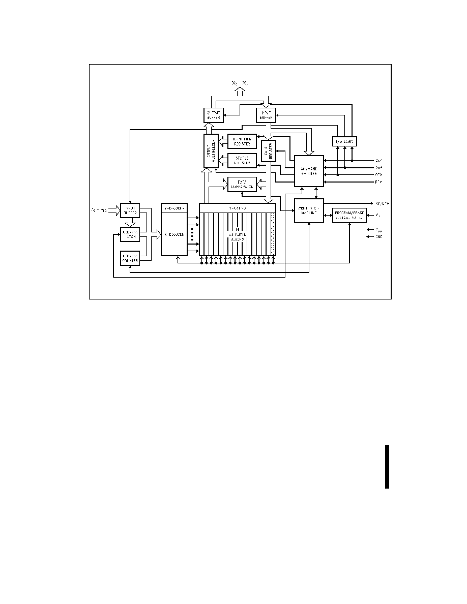
29042901
Figure 1. Block Diagram

E
28F008SA
7
PRELIMINARY
Table 1. Pin Descriptions
Symbol
Type
Name and Function
A
0
≠A
19
INPUT
ADDRESS INPUTS for memory addresses. Addresses are internally
latched during a write cycle.
DQ
0
≠DQ
7
INPUT/OUTPUT
DATA INPUT/OUTPUTS: Inputs data and commands during CUI
write cycles; outputs data during memory array, status register and
Identifier read cycles. The data pins are active high and float to tri-
state off when the chip is deselected or the outputs are disabled. Data
is internally latched during a write cycle.
CE#
INPUT
CHIP ENABLE: Activates the device's control logic, input buffers,
decoders, and sense amplifiers. CE# is active low; CE# high
deselects the memory device and reduces power consumption to
standby levels.
RP#
INPUT
RESET/DEEP POWER-DOWN: Puts the device in deep power-down
mode. RP# is active low; RP# high gates normal operation. RP# also
locks out block erase or byte write operations when active low,
providing data protection during power transitions. RP# active resets
internal automation. Exit from deep power-down sets device to read-
array mode.
OE#
INPUT
OUTPUT ENABLE: Gates the device's outputs through the data
buffers during a read cycle. OE# is active low.
WE#
INPUT
WRITE ENABLE: Controls writes to the CUI and array blocks. WE#
is active low. Addresses and data are latched on the rising edge of
the WE# pulse.
RY/BY#
OUTPUT
READY/BUSY#: Indicates the status of the internal Write State
Machine. When low, it indicates that the WSM is performing a block
erase or byte write operation. RY/BY# high indicates that the WSM is
ready for new commands, block erase is suspended or the device is
in deep power-down mode. RY/BY# is always active and does NOT
float to tri-state off when the chip is deselected or data outputs are
disabled.
V
PP
BLOCK ERASE/BYTE WRITE POWER SUPPLY for erasing blocks
of the array or writing bytes of each block.
NOTE:
With V
PP
< V
PPLMAX
, memory contents cannot be altered.
V
CC
DEVICE POWER SUPPLY (5 V Ī10%, 5 V Ī5%)
GND
GROUND
28F008SA
E
8
PRELIMINARY
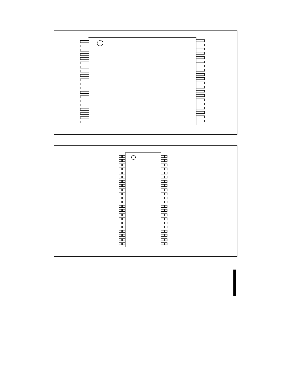
E28F008SA
40-Lead TSOP
10 mm x 20 mm
TOP VIEW
20
19
18
17
16
15
14
13
12
11
10
9
8
7
6
5
4
3
2
1
21
22
23
24
25
26
27
28
29
30
31
32
33
34
35
36
37
38
39
40
A
19
CE#
A
18
A
17
A
16
A
15
A
14
A
13
A
12
V
CC
V
PP
RP#
A
11
A
10
A
9
A
8
A
7
A
6
A
5
A
4
NC
DQ
4
NC
WE#
OE#
RY/BY#
DQ
7
DQ
6
DQ
5
V
CC
GND
GND
DQ
3
DQ
2
DQ
1
DQ
0
A
0
A
1
A
2
A
3
0429_02
Figure 2. TSOP Lead Configurations
PA28F008SA
40-Lead PSOP
0.525" X 1.110"
TOP VIEW
20
19
18
17
16
15
14
13
12
11
10
9
8
7
6
5
4
3
2
1
41
42
25
26
27
28
29
30
31
32
33
34
35
36
37
38
39
40
43
44
V
PP
A
5
RP#
A
11
A
10
A
9
A
8
A
7
A
6
A
4
NC
NC
A
3
A
2
A
1
A
0
DQ
0
DQ
1
DQ
2
DQ
3
V
CC
A
18
CE#
A
12
A
13
A
14
A
15
A
16
A
17
A
19
NC
NC
NC
NC
WE#
OE#
RY/BY#
DQ
7
DQ
6
DQ
5
22
21
23
24
GND
GND
DQ
4
V
CC
0429_03
Figure 3. PSOP Lead Configuration
E
28F008SA
9
PRELIMINARY
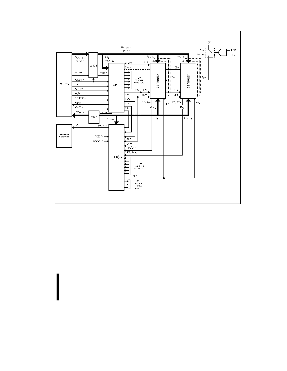
29042905
Figure 4. 28F008SA Array Interface to Intel386SL Microprocessor Superset through PI Bus
(Including RY/BY# Masking and Selective Power-Down), for DRAM Backup during System SUSPEND,
Resident O/S and Applications and Motherboard Solid-State Disk.
28F008SA
E
10
PRELIMINARY
2.0
PRINCIPLES OF OPERATION
The 28F008SA includes on-chip write automation to
manage write and erase functions. The Write State
Machine (WSM) allows for 100% TTL-level control
inputs, fixed power supplies during block erasure
and byte write, and minimal processor overhead
with RAM-like interface timings.
After initial device power-up, or after return from
deep power-down mode (see
Bus Operations), the
28F008SA functions as a read-only memory.
Manipulation of external memory-control pins allow
array read, standby and output disable operations.
Both status register and intelligent identifiers can
also be accessed through the CUI when V
PP
=
V
PPL
.
This same subset of operations is also available
when high voltage is applied to the V
PP
pin. In
addition, high voltage on V
PP
enables successful
block erasure and byte writing of the device. All
functions associated with altering memory
contents--byte write, block erase, status and
intelligent identifier--are accessed via the CUI and
verified through the status register.
Commands are written using standard
microprocessor write timings. CUI contents serve
as input to the WSM, which controls the block erase
and byte write circuitry. Write cycles also internally
latch addresses and data needed for byte write or
block erase operations. With the appropriate
command written to the register, standard
microprocessor read timings output array data,
access the intelligent identifier codes, or output byte
write and block erase status for verification.
Interface software to initiate and poll progress of
internal byte write and block erase can be stored in
any of the 28F008SA blocks. This code is copied
to, and executed from, system RAM during actual
flash memory update. After successful completion
of byte write and/or block erase, code/data reads
from the 28F008SA are again possible via the Read
Array command. Erase suspend/resume capability
allows system software to suspend block erase to
read data and execute code from any other block.
64-Kbyte Block
EFFFF
FFFFF
64-Kbyte Block
64-Kbyte Block
64-Kbyte Block
64-Kbyte Block
64-Kbyte Block
64-Kbyte Block
64-Kbyte Block
64-Kbyte Block
64-Kbyte Block
64-Kbyte Block
64-Kbyte Block
F0000
DFFFF
E0000
CFFFF
D0000
BFFFF
C0000
AFFFF
B0000
9FFFF
A0000
8FFFF
90000
7FFFF
80000
6FFFF
70000
5FFFF
60000
4FFFF
50000
3FFFF
40000
64-Kbyte Block
64-Kbyte Block
64-Kbyte Block
64-Kbyte Block
30000
2FFFF
20000
1FFFF
10000
0FFFF
00000
0429_05
Figure 5. Memory Map

E
28F008SA
11
PRELIMINARY
2.1
Command User Interface and
Write Automation
An on-chip state machine controls block erase and
byte write, freeing the system processor for other
tasks. After receiving the Erase Setup and Erase
Confirm commands, the state machine controls
block pre-conditioning and erase, returning
progress via the status register and RY/BY# output.
Byte write is similarly controlled, after destination
address and expected data are supplied. The
program and erase algorithms of past Intel
ģ
Flash
memories are now regulated by the state machine,
including pulse repetition where required and
internal verification and margining of data.
2.2
Data Protection
Depending on the application, the system designer
may choose to make the V
PP
power supply
switchable (available only when memory byte
writes/block erases are required) or hardwired to
V
PPH
. When V
PP
= V
PPL
, memory contents cannot
be altered. The 28F008SA CUI architecture
provides protection from unwanted byte write or
block erase operations even when high voltage is
applied to V
PP
. Additionally, all functions are
disabled whenever V
CC
is below the write lockout
voltage V
LKO
, or when RP# is at V
IL
. The
28F008SA accommodates either design practice
and encourages optimization of the processor-
memory interface.
The two-step byte write/block erase CUI write
sequence provides additional software write
protection.
3.0
BUS OPERATION
Flash memory reads, erases and writes in-system
via the local CPU. All bus cycles to or from the flash
memory conform to standard microprocessor bus
cycles.
3.1
Read
The 28F008SA has three read modes. The memory
can be read from any of its blocks, and information
can be read from the intelligent identifier or status
register. V
PP
can be at either V
PPL
or V
PPH
.
The first task is to write the appropriate read mode
command to the CUI (array, intelligent identifier, or
status register). The 28F008SA automatically
resets to read array mode upon initial device power-
up or after exit from deep power-down. The
28F008SA has four control pins, two of which must
be logically active to obtain data at the outputs.
Chip Enable (CE#) is the device selection control,
and when active enables the selected memory
device. Output Enable (OE#) is the data
input/output (DQ
0
≠DQ
7
) direction control, and when
active drives data from the selected memory onto
the I/O bus. RP# and WE# must also be at V
IH
.
Figure 13 illustrates read bus cycle waveforms.
3.2
Output Disable
With OE# at a logic-high level (V
IH
), the device
outputs are disabled. Output pins (DQ
0
≠DQ
7
) are
placed in a high-impedance state.
3.3
Standby
CE# at a logic-high level (V
IH
) places the
28F008SA in standby mode. Standby operation
disables much of the 28F008SA's circuitry and
substantially reduces device power consumption.
The outputs (DQ
0
≠DQ
7
) are placed in a high-
impedance state independent of the status of OE#.
If the 28F008SA is deselected during block erase or
byte write, the device will continue functioning and
consuming normal active power until the operation
completes.

28F008SA
E
12
PRELIMINARY
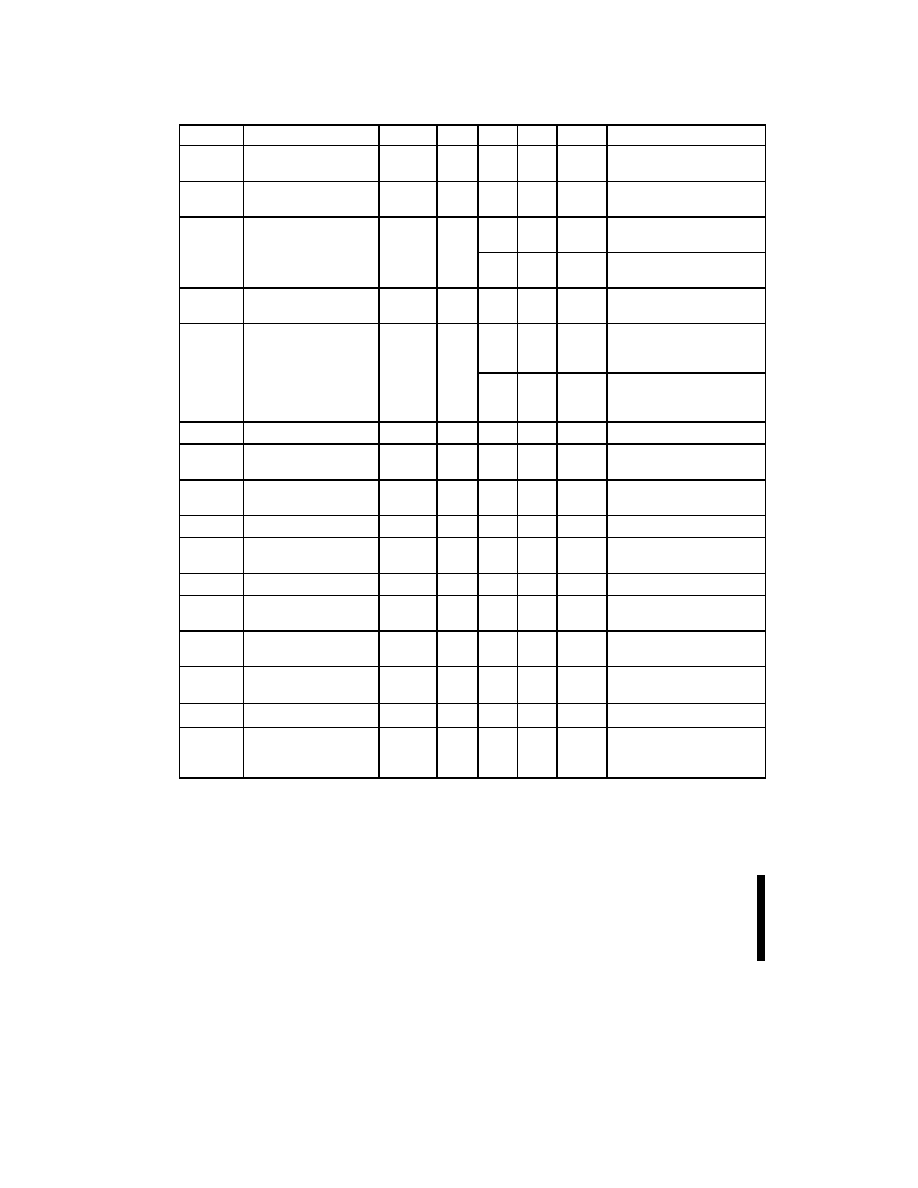
Table 2. Bus Operations
Mode
Notes
RP#
CE#
OE#
WE#
A
0
V
PP
DQ
0
≠
7
RY/BY#
Read
1, 2, 3
V
IH
V
IL
V
IL
V
IH
X
X
D
OUT
X
Output Disable
1, 2, 3
V
IH
V
IL
V
IH
V
IH
X
X
High Z
X
Standby
1, 2, 3
V
IH
V
IH
X
X
X
X
High Z
X
Deep Power-
Down
1, 2
V
IL
X
X
X
X
X
High Z
V
OH
Intelligent
Identifier (Mfr)
1, 2
V
IH
V
IL
V
IL
V
IH
V
IL
X
89H
V
OH
Intelligent
Identifier
(Device)
1, 2
V
IH
V
IL
V
IL
V
IH
V
IH
X
A2H
V
OH
Write
1,2,3,4,5
V
IH
V
IL
V
IH
V
IL
X
X
D
IN
X
NOTES:
1.
Refer to
DC Characteristics. When V
PP
= V
PPL
, memory contents can be read but not written or erased.
2.
X can be V
IL
or V
IH
for control pins and addresses, and V
PPL
or V
PPH
for V
PP
. See
DC Characteristics for V
PPL
and V
PPH
voltages.
3.
RY/BY# is V
OL
when the Write State Machine is executing internal block erase or byte write algorithms. It is V
OH
when the
WSM is not busy, in erase suspend mode or deep power-down mode.
4.
Command writes involving block erase or byte write are only successfully executed when V
PP
= V
PPH
.
5.
Refer to Table 3 for valid D
IN
during a write operation.
3.4
Deep Power-Down
The 28F008SA offers a deep power-down feature,
entered when RP# is at V
IL
. Current draw through
V
CC
is 0.20 ĶA typical in deep power-down mode,
with current draw through V
PP
typically 0.1 ĶA.
During read modes, RP#-low deselects the
memory, places output drivers in a high-impedance
state and turns off all internal circuits. The
28F008SA requires time t
PHQV
(see
AC
Characteristics-Read-Only Operations) after return
from power-down until initial memory access
outputs are valid. After this wakeup interval, normal
operation is restored. The CUI is reset to Read
Array, and the upper 5 bits of the status register are
cleared to value 10000, upon return to normal
operation.
During block erase, program or lock-bit
configuration, RP#-low will abort the operation.
RY/BY# remains low until the reset operation is
complete. Memory contents being altered are no
longer valid; the data may be partially erased or
written. Time t
PHWL
is required after RP# goes to
logic-high (V
IH
) before another command can be
written.
This use of RP# during system reset is important
with automated write/erase devices. When the
system comes out of reset it expects to read from
the flash memory. Automated flash memories
provide status information when accessed during
write/erase modes. If a CPU
reset occurs with no
flash memory reset, proper CPU initialization would
not
occur because the flash memory would be
providing the status information
instead of array
data. Intel's Flash memories allow proper CPU
initialization
following a system reset through the
use of the RP# input. In this
application RP# is
controlled by the same RESET# signal that resets
the
system CPU.
3.5
Intelligent Identifier Operation
The intelligent identifier operation outputs the
manufacturer code, 89H; and the device code, A2H
for the 28F008SA. The system CPU can then
automatically match the device with its proper block
erase and byte write algorithms.

E
28F008SA
13
PRELIMINARY
The manufacturer- and device-codes are read via
the CUI. Following a write of 90H to the CUI, a read
from address location 00000H outputs the
manufacturer code (89H). A read from address
00001H outputs the device code (A2H). It is not
necessary to have high voltage applied to V
PP
to
read the intelligent identifiers from the CUI.
3.6
Write
Writes to the CUI enable reading of device data and
Intelligent Identifiers. They also control inspection
and clearing of the status register. Additionally,
when V
PP
= V
PPH
, the CUI controls block erasure
and byte write. The contents of the interface
register serve as input to the internal state machine.
The CUI itself does not occupy an addressable
memory location. The interface register is a latch
used to store the command and address and data
information needed to execute the command. Erase
Setup and Erase Confirm commands require both
appropriate command data and an address within
the block to be erased. The Byte Write Setup
command requires both appropriate command data
and the address of the location to be written, while
the Byte Write command consists of the data to be
written and the address of the location to be written.
The CUI is written by bringing WE# to a logic-low
level (V
IL
) while CE# is low. Addresses and data
are latched on the rising edge of WE#. Standard
microprocessor write timings are used.
Refer to
AC Write Characteristics and the AC
Waveforms for Write Operations, Figure 15, for
specific timing parameters.
4.0
COMMAND DEFINITIONS
When V
PPL
is applied to the V
PP
pin, read
operations from the status register, intelligent
identifiers, or array blocks are enabled. Placing
V
PPH
on V
PP
enables successful byte write and
block erase operations as well.
Device operations are selected by writing specific
commands into the CUI. Table 3 defines the
28F008SA commands.
4.1
Read Array Command
Upon initial device power-up and after exit from
deep power-down mode, the 28F008SA defaults to
read array mode. This operation is also initiated by
writing FFH into the CUI. Microprocessor read
cycles retrieve array data. The device remains
enabled for reads until the CUI contents are altered.
Once the internal WSM has started a block erase or
byte write operation, the device will not recognize
the Read Array command, until the WSM has
completed its operation. The Read Array command
is functional when V
PP
= V
PPL
or V
PPH
.
28F008SA
E
14
PRELIMINARY
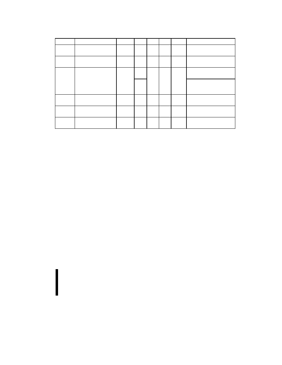
Table 3. Command Definitions
Command
Bus
Cycles
Req'd
Notes
First Bus Cycle
Second Bus Cycle
Oper
(1)
Addr
(2)
Data
(3)
Oper
(1)
Addr
(2)
Data
(3)
Read Array/Reset
1
Write
X
FFH
Intelligent Identifier
3
4
Write
X
90H
Read
IA
IID
Read Status Register
2
Write
X
70H
Read
X
SRD
Clear Status Register
1
Write
X
50H
Erase Setup/Erase
Confirm
2
Write
BA
20H
Write
BA
D0H
Erase Suspend/Erase
Resume
2
Write
X
B0H
Write
X
D0H
Byte Write Setup/Write
2
5
Write
WA
40H
Write
WA
WD
Alternate Byte Write
Setup/Write
2
5
Write
WA
10H
Write
WA
WD
NOTES:
1.
Bus operations are defined in Table 2.
2.
IA = Identifier Address: 00H for manufacturer code, 01H for device code.
BA = Address within the block being erased.
WA = Address of memory location to be written.
3.
SRD = Data read from status register. See Table 4 for a description of the status register bits.
WD = Data to be written at location WA. Data is latched on the rising edge of WE#.
IID = Data read from Intelligent Identifiers.
4.
Following the Intelligent Identifier command, two read operations access manufacture and device codes.
5.
Either 40H or 10H are recognized by the WSM as the Byte Write Setup command.
6.
Commands other than those shown above are reserved by Intel for future device implementations and should not be used.

E
28F008SA
15
PRELIMINARY
4.2
Intelligent Identifier Command
The 28F008SA contains an intelligent identifier
operation, initiated by writing 90H into the CUI.
Following the command write, a read cycle from
address 00000H retrieves the manufacturer code of
89H. A read cycle from address 00001H returns the
device code of A2H. To terminate the operation, it
is necessary to write another valid command into
the register. Like the Read Array command, the
Intelligent Identifier command is functional when
V
PP
= V
PPL
or V
PPH
.
4.3
Read Status Register
Command
The 28F008SA contains a status register which
may be read to determine when a byte write or
block erase operation is complete, and whether that
operation completed successfully. The status
register may be read at any time by writing the
Read Status Register command (70H) to the CUI.
After writing this command, all subsequent read
operations output data from the status register, until
another valid command is written to the CUI. The
contents of the status register are latched on the
falling edge of OE# or CE#, whichever occurs last
in the read cycle. OE# or CE# must be toggled to
V
IH
before further reads to update the status
register latch. The Read Status Register command
functions when V
PP
= V
PPL
or V
PPH
.
4.4
Clear Status Register
Command
The erase status and byte write status bits are set
to "1"s by the Write State Machine and can only be
reset by the Clear Status Register command.
These bits indicate various failure conditions (see
Table 4). By allowing system software to control the
resetting of these bits, several operations may be
performed (such as cumulatively writing several
bytes or erasing multiple blocks in sequence). The
status register may then be polled to determine if
an error occurred during that sequence. This adds
flexibility to the way the device may be used.
Additionally, the V
PP
status bit (SR.3) must be
reset by system software before further byte writes
or block erases are attempted. To clear the Status
Register, the Clear Status Register command (50H)
is written to the CUI. The Clear Status Register
command is functional when V
PP
= V
PPL
or V
PPH
.
4.5
Erase Setup/Erase Confirm
Commands
Erase is executed one block at a time, initiated by a
two-cycle command sequence. An Erase Setup
command (20H) is first written to the CUI, followed
by the Erase Confirm command (D0H). These
commands require both appropriate sequencing
and an address within the block to be erased to
FFH. Block preconditioning, erase and verify are all
handled internally by the WSM, invisible to the
system. After the two-command erase sequence is
written to it, the 28F008SA automatically outputs
status register data when read (see Figure 6;
Automated Block Erase Flowchart). The CPU can
detect the completion of the erase event by
analyzing the output of the RY/BY# pin, or the
WSM status bit of the status register.
When erase is completed, the erase status bit
should be checked. If erase error is detected, the
status register should be cleared. The CUI remains
in read status register mode until further commands
are issued to it.
This two-step sequence of set-up followed by
execution ensures that memory contents are not
accidentally erased. Also, reliable block erasure
can only occur when V
PP
= V
PPH
. In the absence of
this high voltage, memory contents are protected
against erasure. If block erase is attempted while
V
PP
= V
PPL
, the V
PP
status bit will be set to "1."
Erase attempts while V
PPL
< V
PP
< V
PPH
produce
spurious results and should not be attempted.
4.6
Erase Suspend/Erase Resume
Commands
The Erase Suspend command allows block erase
interruption in order to read data from another block
of memory. Once the erase process starts, writing
the erase suspend command (B0H) to the CUI
requests that the WSM suspend the erase
sequence at a predetermined point in the erase
algorithm. The 28F008SA continues to output
status register data when read, after the Erase
Suspend command is written to it. Polling the WSM
status and erase suspend status bits will determine
when the erase operation has been suspended
(both will be set to "1"). RY/BY# will also transition
to V
OH
.

28F008SA
E
16
PRELIMINARY
At this point, a Read Array command can be written
to the CUI to read data from blocks other than that
which is suspended. The only other valid
commands at this time are Read Status Register
(70H) and Erase Resume (D0H), at which time the
WSM will continue with the erase process. The
erase suspend status and WSM status bits of the
status register will be automatically cleared and
RY/BY# will return to V
OL
. After the Erase Resume
command is written to it, the 28F008SA
automatically outputs status register data when
read (see Figure 7
; Erase Suspend/Resume
Flowchart). V
PP
must remain at V
PPH
while the
28F008SA is in Erase Suspend.
4.7
Byte Write Setup/Write
Commands (40H or 10H)
Byte write is executed by a two-command
sequence. The Byte Write Setup command (40H or
10H) is written to the CUI, followed by a second
write specifying the address and data (latched on
the rising edge of WE#) to be written. The WSM
then takes over, controlling the byte write and write
verify algorithms internally. After the two-command
byte write sequence is written to it, the 28F008SA
automatically outputs status register data when
read (see Figure 8;
Automated Byte Write
Flowchart). The CPU can detect the completion of
the byte write event by analyzing the output of the
RY/BY# pin, or the WSM status bit of the status
register. Only the Read Status Register command
is valid while byte write is active.
When byte write is complete, the byte write status
bit should be checked. If byte write error is
detected, the status register should be cleared. The
internal WSM verify only detects errors for "1"s that
do not successfully write to "0"s. The CUI remains
in read status register mode until further commands
are issued to it. If byte write is attempted while V
PP
= V
PPL
, the V
PP
status bit will be set to "1." Byte
write attempts while V
PPL
< V
PP
< V
PPH
produce
spurious results and should not be attempted.
5.0
EXTENDED BLOCK
ERASE/BYTE WRITE CYCLING
Intel has designed extended cycling capability into
its ETOX flash memory technologies. The
28F008SA is designed for 100,000 byte write/block
erase cycles on each of the sixteen 64-Kbyte
blocks. Low electric fields, advanced oxides and
minimal oxide area per cell subjected to the
tunneling electric field combine to greatly reduce
oxide stress and the probability of failure. A 20-
Mbyte solid-state drive using an array of
28F008SAs has a MTBF (Mean Time Between
Failure) of 33.3 million hours
1
, over 600 times more
reliable than equivalent rotating disk technology.
6.0
AUTOMATED BYTE WRITE
The 28F008SA integrates the Quick-Pulse
programming algorithm of prior Intel Flash devices
on-chip, using the CUI, status register and WSM.
On-chip integration dramatically simplifies system
software and provides processor interface timings
to the CUI and status register. WSM operation,
internal verify and V
PP
high voltage presence are
monitored and reported via the RY/BY# output and
appropriate status register bits. Figure 8,
Automated Byte Write Flowchart, shows a system
software flowchart for device byte write. The entire
sequence is performed with V
PP
at V
PPH
. Byte write
abort occurs when RP# transitions to V
IL
, or V
PP
drops
to V
PPL
. Although the WSM is halted, byte
data is partially written at
the location where byte
write was aborted. Block erasure, or a repeat of
byte write, is required to initialize this data to a
known value.
7.0
AUTOMATED BLOCK ERASE
As above, the Quick-Erase algorithm of prior Intel
Flash devices is now implemented internally,
including all preconditioning of block data. WSM
operation, erase success and V
PP
high voltage
presence are monitored and reported through
RY/BY# and the status register. Additionally, if a
command other than Erase Confirm is written to the
device following Erase Setup, both the Erase status
and Byte Write status bits will be set to "1"s. When
issuing the Erase Setup and Erase Confirm
commands, they should be written to an address
within the address range of the block to be erased.
Figure 6,
Automated Block Erase Flowchart, shows
a system software flowchart for block erase.
1
Assumptions: 10-Kbyte file written every 10 minutes. (20-Mbyte
array)/(10-Kbyte file) = 2,000 file writes before erase required.
(2000 files writes/erase) ◊ (100,000 cycles per 28F008SA block) =
200 million file writes.
(200 ◊ 10
6
file writes) ◊ (10 min/write) ◊ (1 hr/60 min) = 33.3 ◊ 10
6
MTBF.

E
28F008SA
17
PRELIMINARY
Erase typically takes 1.6 seconds per block. The
Erase Suspend/Erase Resume command sequence
allows suspension of this erase operation to read
data from a block other than that in which erase is
being performed. A system software flowchart is
shown in Figure 7,
Erase Suspend/Resume
Flowchart.
The entire sequence is performed with V
PP
at
V
PPH
. Abort occurs when RP# transitions to V
IL
or
V
PP
falls to V
PPL
, while erase is in progress. Block
data is partially erased by this operation, and a
repeat of erase is required to obtain a fully erased
block.
8.0
DESIGN CONSIDERATIONS
8.1
Three-Line Output Control
The 28F008SA will often be used in large memory
arrays. Intel provides three control inputs to
accommodate multiple memory connections. Three-
line control provides for:
a) lowest possible memory power dissipation
b) complete assurance that data bus contention
will not occur
To efficiently use these control inputs, an address
decoder should enable CE#, while OE# should be
connected to all memory devices and the system's
READ# control line. This assures that only selected
memory devices have active outputs while
deselected memory devices are in
standby mode.
RP# should be connected to the system
POWERGOOD signal to prevent unintended writes
during system power transitions. POWERGOOD
should also toggle during system reset.
8.2
RY/BY# and Byte Write/Block
Erase Polling
RY/BY# is a full CMOS output that provides a
hardware method of detecting byte write and block
erase completion. It transitions low time t
WHRL
after
a write or erase command sequence is written to
the 28F008SA, and returns to V
OH
when the WSM
has finished executing the
internal algorithm.
RY/BY# can be connected to the interrupt input of
the system CPU or controller. It is active at all
times, not tri-stated if the 28F008SA CE# or OE#
inputs are brought to V
IH
. RY/BY# is also V
OH
when
the device is in erase suspend or deep power-down
modes.
8.3
Power Supply Decoupling
Flash memory power switching characteristics
require careful device decoupling. System
designers are interested in three supply current
issues; standby current levels (I
SB
), active current
levels (I
CC
) and transient peaks produced by falling
and rising edges of CE#. Transient current
magnitudes depend on the device outputs'
capacitive and inductive loading. Two-line control
and proper decoupling capacitor selection will
suppress transient voltage peaks. Each device
should have a 0.1 ĶF ceramic capacitor connected
between each V
CC
and GND, and between its V
PP
and GND. These high frequency, low inherent-
inductance capacitors should be placed as close as
possible to package leads. Additionally, for every
eight devices, a 4.7 ĶF electrolytic capacitor should
be placed at the array's power supply connection
between V
CC
and GND. The bulk capacitor will
overcome voltage slumps caused by PC board
trace inductances.

28F008SA
E
18
PRELIMINARY
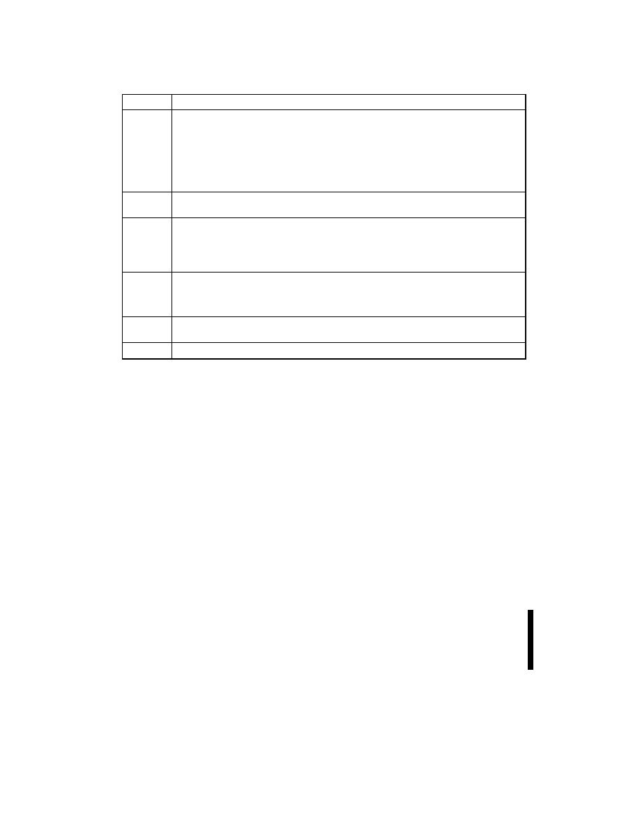
Table 4. Status Register Definitions
WSMS
ESS
ES
BWS
VPPS
R
R
R
7
6
5
4
3
2
1
0
NOTES:
R.7 = WRITE STATE MACHINE STATUS
1 = Ready
0 = Busy
RY/BY# or the Write State Machine status bit must
first be checked to determine byte write or block
erase completion, before the Byte Write or Erase
status bit are checked for success.
SR.6 = ERASE SUSPEND STATUS
1 = Erase Suspended
0 = Erase in Progress/Completed
SR.5 = ERASE STATUS
1 = Error in Block Erasure
0 = Successful Block Erase
SR.4 = BYTE WRITE STATUS
1 = Error in Byte Write
0 = Successful Byte Write
If the Byte Write and Erase status bits are set to
"1"s during a block erase attempt, an improper
command sequence was entered. Attempt the
operation again.
SR.3 = V
PP
STATUS
1 = V
PP
Low Detect; Operation Abort
0 = V
PP
OK
If V
PP
low status is detected, the status register
must be cleared before another byte write or block
erase operation is attempted.
The V
PP
status bit, unlike an A/D converter, does
not provide continuous indication of V
PP
level. The
WSM interrogates the V
PP
level only after the byte
write or block erase command sequences have
been entered and informs the system if V
PP
has
not been switched on. The V
PP
status bit is not
guaranteed to report accurate feedback between
V
PPL
and V
PPH
.
SR.2≠SR.0 = RESERVED FOR FUTURE
ENHANCEMENTS
These bits are reserved for future use and should
be masked out when polling the status register.

E
28F008SA
19
PRELIMINARY
Start
Write 20H,
Block Address
Write D0H,
Block Address
WSM Ready?
Full Status
Check if Desired
Block Erase
Completed
Read Status
Register Data
(See Above)
V
PP
Range Error
Command Sequence
Error
SR.3 = 0?
SR.4, 5 = 1?
FULL STATUS CHECK PROCEDURE
Bus
Operation
Write
Write
Standby/Read
Repeat for subsequent bytes.
Full status check can be done after each byte, or after a sequence of
bytes.
Write FFH after the last byte write operation to reset the device to read
array mode.
Bus
Operation
Standby
Standby
SR.3 must be cleared, if set during a block erase attempt, before
further attempts are allowed by the Write State Machine.
SR.5 is only cleared by the clear status register command in cases
where multiple bytes are erased before full status is checked.
If an error is detected, clear the status register before attempting retry
or other error recovery.
Yes
No
Yes
No
Yes
Command
Erase Setup
Erase
Comments
Data = 40H (10H)
Addr = Within Block to Be Erased
Data = D0H
Addr = Within Block to Be Erased
Check RY/BY#
(V
OH
= Ready, V
OL
= Busy)
or
Read Status Register
(Check SR.7
1 = Ready, 0 = Busy
Toggle OE# or CE# to Update
Status Register)
Command
Comments
Check SR.3
1 = V
PP
Low Detect
Check SR.5
1 = Block Erase Error
Optional Read
CPU may already have read status
register data in WSM Ready polling
above
Suspend
Erase?
No
Yes
Erase Suspend
Loop
No
Block Erase Error
Byte Write
Successful
SR.5 = 0?
Yes
No
Standby
Check SR.4, 5
Both 1 = Command Sequence
Error
0429_07
Figure 6. Automated Block Erase Flowchart
28F008SA
E
20
PRELIMINARY
Write 70H
Read Status Register
SR.7 = 1?
SR.6 = 1?
Done Reading?
Write D0H
Continue Erase
No
Yes
Yes
Yes
No
No
Bus
Operation
Command
Comments
Write
Erase Suspend Data = B0H
Write
Read Status
Register
Data = 70H
Standby/Read
Check RY/BY#
(V
OH
= Ready, V
OL
= Busy)
or
Read Status Register
(Check SR.7
1 = Ready, 0 = Busy
Toggle OE# or CE# to
update Status Register)
Start
Write B0H
Write FFH
Erase Has Completed
Standby
Check SR.6
1 = Suspended
Write
Read Array
Data = FFH
Write
Erase Resume
Data = D0H
Read
Read array data from block
other than that being
erased
0429_08
Figure 7. Erase Suspend/Resume Flowchart
E
28F008SA
21
PRELIMINARY
Start
Write 40H (10H),
Byte Address
Write Byte
Address/Data
WSM Ready?
Full Status
Check if Desired
Byte Write
Completed
Read Status
Register Data
(See Above)
V
PP
Range Error
Byte Write Error
Byte Write
Successful
SR.3 = 0?
SR.4 = 0?
FULL STATUS CHECK PROCEDURE
Bus
Operation
Write
Write
Standby/Read
Repeat for subsequent bytes.
Full status check can be done after each byte, or after a sequence of
bytes.
Write FFH after the last byte write operation to reset the device to read
array mode.
Bus
Operation
Standby
Standby
SR.3 must be cleared, if set during a byte write attempt, before further
attempts are allowed by the Write State Machine.
SR.4 is only cleared by the clear status register command in cases
where multiple bytes are written before full status is checked.
If an error is detected, clear the status register before attempting retry
or other error recovery.
No
Yes
No
Yes
No
Yes
Command
Byte Write
Setup
Byte Write
Comments
Data = 40H (10H)
Addr = Byte to Be Written
Data to Be Wriiten
Addr = Byte to Be Written
Check RY/BY#
(V
OH
= Ready, V
OL
= Busy)
or
Read Status Register
(Check SR.7
1 = Ready, 0 = Busy
Toggle OE# or CE# to Update
Status Register)
Command
Comments
Check SR.3
1 = V
PP
Low Detect
Check SR.4
1 = Byte Write Error
Optional Read
CPU may already have read status
register data in WSM Ready polling
above
0429_06
Figure 8. Automated Byte Write Flowchart

28F008SA
E
22
PRELIMINARY
8.4
V
PP
Trace on Printed Circuit
Boards
Writing flash memories, while they reside in the
target system, requires that the printed circuit board
designer pay attention to the V
PP
power supply
trace. The V
PP
pin supplies the memory cell current
for writing and erasing. Use similar trace widths and
layout considerations given to the V
CC
power bus.
Adequate V
PP
supply traces and decoupling will
decrease V
PP
voltage spikes and overshoots.
8.5
V
CC
, VPP, RP# Transitions and
the Command/Status Registers
Byte write and block erase completion are not
guaranteed if V
PP
drops below V
PPH
. If the V
PP
status bit of the status register (SR.3) is set to "1," a
Clear Status Register command must be issued
before further byte write/block erase attempts are
allowed by the WSM. Otherwise, the byte write
(SR.4) or erase (SR.5) status bits of the status
register will be set to "1"s if error is detected. If RP#
transitions to V
IL
during byte write and block erase,
RY/BY# will remain low until the reset operation is
complete. Data is partially altered in either case,
and the command sequence must be repeated after
normal operation is restored. Device power-off, or
RP# transitions to V
IL
, clear the status register to
initial value 10000 for the upper 5 bits.
The CUI latches commands as issued by system
software and is not altered by V
PP
or CE#
transitions or WSM actions. Its state upon power-
up, after exit from deep power-down or after V
CC
transitions below V
LKO
, is read array mode.
After byte write or block erase is complete, even
after V
PP
transitions down to V
PPL
, the CUI must be
reset to read array mode via the Read Array
command if access to the memory array is desired.
8.6
Power Up/Down Protection
The 28F008SA is designed to offer protection
against accidental block erasure or byte writing
during power transitions. Upon power-up, the
28F008SA is indifferent as to which power supply,
V
PP
or V
CC
, powers up first. Power supply
sequencing is not required. Internal circuitry in the
28F008SA ensures that the CUI is reset to the read
array mode on power-up.
A system designer must guard against spurious
writes for V
CC
voltages above V
LKO
when V
PP
is
active. Since both WE# and CE# must be low for a
command write, driving either to V
IH
will inhibit
writes. The CUI architecture provides an added
level of protection since alteration of memory
contents only occurs after successful completion of
the two-step command sequences.
Finally, the device is disabled until RP# is brought
to V
IH
, regardless of the state of its control inputs.
This provides an additional level of memory
protection.
8.7
Power Dissipation
When designing portable systems, designers must
consider battery power consumption not only during
device operation, but also for data retention during
system idle time. Flash nonvolatility increases
usable battery life, because the 28F008SA does not
consume any power to retain code or data when the
system is off.
In addition, the 28F008SA's deep power-down
mode ensures extremely low power dissipation
even when system power is applied. For example,
portable PCs and other power sensitive
applications, using an array of 28F008SAs for solid-
state storage, can lower RP# to V
IL
in standby or
sleep modes, producing negligible power
consumption. If access to the 28F008SA is again
needed, the part can again be read, following the
t
PHQV
and t
PHWL
wakeup cycles required after RP#
is first raised back to V
IH
. See AC Characteristics--
Read-Only and Write Operations and Figures 13
and 15 for more information.

E
28F008SA
23
PRELIMINARY
9.0
ELECTRICAL SPECIFICATIONS
9.1
Absolute Maximum Ratings*
Operating Temperature
During Read............................ 0 įC to +70 įC
(1)
During Block Erase/Byte Write ... 0 įC to +70 įC
Temperature Under Bias ...............≠10 įC to +80 įC
Storage Temperature ..................≠65 įC to +125 įC
Voltage on Any Pin
(except V
CC
and V
PP
)
with Respect to GND............ ≠2.0 V to +7.0 V
(2)
V
PP
Program Voltage with
Respect to GND during
Block Erase/Byte Write ....≠2.0 V to +14.0 V
(2, 3)
V
CC
Supply Voltage
with Respect to GND ..... ≠2.0 V to +7.0 V
(2)
Output Short Circuit Current .....................100 mA
(4)
NOTICE: This datasheet contains preliminary information on
new products in production. The specifications are subject
to change without notice. Verify with your local Intel Sales
office that you have the latest datasheet before finalizing a
design.
*WARNING: Stressing the device beyond the "Absolute
Maximum Ratings" may cause permanent damage. These
are stress ratings only. Operation beyond the "Operating
Conditions" is not recommended and extended exposure
beyond the "Operating Conditions" may affect device
reliability.
NOTES:
1.
Operating temperature is for commercial product
defined by this specification.
2.
Minimum DC voltage is ≠0.5 V on input/output pins.
During transitions, this level may undershoot to ≠2.0 V
for periods
<20 ns. Maximum DC voltage on input/output pins is
V
CC
+ 0.5 V which, during transitions, may overshoot to
V
CC
+ 2.0 V for periods <20 ns.
3.
Maximum DC voltage on V
PP
may overshoot to +14.0 V
for periods <20 ns.
4.
Output shorted for no more than one second. No more
than one output shorted at a time.
5.
5% V
CC
specifications reference the 28F008SA-85 in
its High Speed configuration. 10% V
CC
specifications
reference the 28F008SA-85 in its Standard
configuration, and the 28F008SA-120.
9.2
Operating Conditions
Symbol
Parameter
Notes
Min
Max
Unit
T
A
Operating Temperature
0
70
įC
V
CC
V
CC
Supply Voltage (10%)
5
4.50
5.50
V
V
CC
V
CC
Supply Voltage (5%)
5
4.75
5.25
V
9.3
Capacitance
(1)
T
A
= 25 įC, f = 1 MHz
Symbol
Parameter
Typ
Max
Unit
Condition
C
IN
Input Capacitance
6
8
pF
V
IN
= 0 V
C
OUT
Output Capacitance
8
12
pF
V
OUT
= 0 V
NOTE:
1.
Sampled, not 100% tested.

28F008SA
E
24
PRELIMINARY
9.4
DC Characteristics
Symbol
Parameter
Notes
Min
Typ
Max
Unit
Test Condition
I
LI
Input Load Current
1
Ī1.0
ĶA
V
CC
= V
CC
Max
V
IN
= V
CC
or GND
I
LO
Output Leakage
Current
1
Ī10
ĶA
V
CC
= V
CC
Max
V
OUT
= V
CC
or GND
I
CCS
V
CC
Standby Current
1, 3
1.0
2.0
mA
V
CC
= V
CC
Max
CE# = RP# = V
IH
30
100
ĶA
V
CC
= V
CC
Max
CE# = RP# = V
CC
Ī0.2 V
I
CCD
V
CC
Deep Power-Down
Current
1
0.20
1.2
ĶA
RP# = GND Ī0.2 V
I
OUT
(RY/BY#) = 0 mA
I
CCR
V
CC
Read Current
1
20
35
mA
V
CC
= V
CC
Max, CE# = GND
f = 8 MHz, I
OUT
= 0 mA
CMOS Inputs
25
50
mA
V
CC
= V
CC
Max, CE# = V
IL
f = 8 MHz, I
OUT
= 0 mA
TTL Inputs
I
CCW
V
CC
Byte Write Current
1
10
30
mA
Byte Write In Progress
I
CCE
V
CC
Block Erase
Current
1
10
30
mA
Block Erase In Progress
I
CCES
V
CC
Erase Suspend
Current
1, 2
5
10
mA
Block Erase Suspended
CE# = V
IH
I
PPS
V
PP
Standby Current
1
Ī1
Ī15
ĶA
V
PP
V
CC
I
PPD
V
PP
Deep Power-Down
Current
1
0.10
5.0
ĶA
RP# = GND Ī0.2 V
I
PPR
V
PP
Read Current
200
ĶA
V
PP
> V
CC
I
PPW
V
PP
Byte Write Current
1
10
30
mA
V
PP
= V
PPH
Byte Write in Progress
I
PPE
V
PP
Block Erase
Current
1
10
30
mA
V
PP
= V
PPH
Block Erase in Progress
I
PPES
V
PP
Erase Suspend
Current
1
90
200
ĶA
V
PP
= V
PPH
Block Erase Suspended
V
IL
Input Low Voltage
≠0.5
0.8
V
V
IH
Input High Voltage
2.0
V
CC
+
0.5
V

E
28F008SA
25
PRELIMINARY
9.4
DC Characteristics
(Continued)
Symbol
Parameter
Notes
Min
Typ
Max
Unit
Test Condition
V
OL
Output Low Voltage
3
0.45
V
V
CC
= V
CC
Min
I
OL
= 5.8 mA
V
OH1
Output High Voltage
(TTL)
3
2.4
V
V
CC
= V
CC
Min
I
OH
= ≠2.5 mA
V
OH2
Output High Voltage
(CMOS)
0.85
V
CC
V
V
CC
= V
CC
Min
I
OH
= ≠2.5 ĶA
V
CC
≠ 0.4
V
CC
= V
CC
Min
I
OH
= ≠100 ĶA
V
PPL
V
PP
during Normal
Operations
4
0.0
6.5
V
V
PPH
V
PP
during Erase/Write
Operations
11.4
12.0
12.6
V
V
LKO
V
CC
Erase/Write Lock
Voltage
2.0
V
NOTES:
1.
All currents are in RMS unless otherwise noted. Typical values at V
CC
= 5.0 V, V
PP
= 12.0 V, T
A
= 25 įC. These currents
are valid for all product versions (packages and speeds).
2.
I
CCES
is specified with the device deselected. If the 28F008SA is read while in erase suspend mode, current draw is the
sum of I
CCES
and I
CCR
.
3.
Includes RY/BY#.
4.
Block erases/byte writes are inhibited when V
PP
= V
PPL
and not guaranteed in the range between V
PPH
and V
PPL
.
5.
Sampled, not 100% tested.
9.5
Extended Temperature Operating Conditions
Symbol
Parameter
Notes
Min
Max
Unit
T
A
Operating Temperature
≠40
+85
įC
V
CC
V
CC
Supply Voltage (10%)
5
4.50
5.50
V
V
CC
V
CC
Supply Voltage (5%)
5
4.75
5.25
V
28F008SA
E
26
PRELIMINARY
9.6
DC Characteristics--Extended Temperature Operation
Symbol
Parameter
Notes
Min
Typ
Max
Unit
Test Condition
I
LI
Input Load Current
1
Ī1.0
ĶA
V
CC
= V
CC
Max
V
IN
= V
CC
or GND
I
LO
Output Leakage
Current
1
Ī10
ĶA
V
CC
= V
CC
Max
V
OUT
= V
CC
or GND
I
CCS
V
CC
Standby Current
1, 3
1.0
2.0
mA
V
CC
= V
CC
Max
CE# = RP# = V
IH
30
100
ĶA
V
CC
= V
CC
Max
CE# = RP# = V
CC
Ī0.2 V
I
CCD
V
CC
Deep Power-Down
Current
1
0.20
20
ĶA
RP# = GND Ī0.2 V
I
OUT
(RY/BY#) = 0 mA
I
CCR
V
CC
Read Current
1
20
35
mA
V
CC
= V
CC
Max, CE# =
GND f = 8 MHz, I
OUT
= 0
mA CMOS Inputs
25
50
mA
V
CC
= V
CC
Max, CE# = V
IL
f = 8 MHz, I
OUT
= 0 mA
TTL Inputs
I
CCW
V
CC
Byte Write Current
1
10
30
mA
Byte Write In Progress
I
CCE
V
CC
Block Erase
Current
1
10
30
mA
Block Erase In Progress
I
CCES
V
CC
Erase Suspend
Current
1, 2
5
10
mA
Block Erase Suspended
CE# = V
IH
I
PPS
V
PP
Standby Current
1
Ī1
Ī15
ĶA
V
PP
V
CC
I
PPD
V
PP
Deep Power-Down
Current
1
0.10
5.0
ĶA
RP# = GND Ī0.2 V
I
PPR
V
PP
Read Current
200
ĶA
V
PP
> V
CC
I
PPW
V
PP
Byte Write Current
1
10
30
mA
V
PP
= V
PPH
Byte Write in Progress
I
PPE
V
PP
Block Erase
Current
1
10
30
mA
V
PP
= V
PPH
Block Erase in Progress
I
PPES
V
PP
Erase Suspend
Current
1
90
200
ĶA
V
PP
= V
PPH
Block Erase Suspended
V
IL
Input Low Voltage
≠0.5
0.8
V
V
IH
Input High Voltage
2.0
V
CC
+
0.5
V
E
28F008SA
27
PRELIMINARY
9.6
DC Characteristics--Extended Temperature Operation
(Continued)
Symbol
Parameter
Notes
Min
Typ
Max
Unit
Test Condition
V
OL
Output Low Voltage
3
0.45
V
V
CC
= V
CC
Min
I
OL
= 5.8 mA
V
OH
1
Output High Voltage
(TTL)
3
2.4
V
V
CC
= V
CC
Min
I
OH
= ≠2.5 mA
V
OH
2
Output High Voltage
(CMOS)
0.85
V
CC
V
V
CC
= V
CC
Min
I
OH
= ≠2.5 ĶA
V
CC
≠
0.4
V
CC
= V
CC
Min
I
OH
= ≠100 ĶA
V
PPL
V
PP
during Normal
Operations
4
0.0
6.5
V
V
PPH
V
PP
during Erase/Write
Operations
11.4
12.0
12.6
V
V
LKO
V
CC
Erase/Write Lock
Voltage
2.0
V
NOTES:
1.
All currents are in RMS unless otherwise noted. Typical values at V
CC
= 5.0 V, V
PP
= 12.0 V, T
A
= 25 įC. These currents
are valid for all product versions (packages and speeds).
2.
I
CCES
is specified with the device deselected. If the 28F008SA is read while in erase suspend mode, current draw is the
sum of I
CCES
and I
CCR
.
3.
Includes RY/BY#.
4.
Block erases/byte writes are inhibited when V
PP
= V
PPL
and not guaranteed in the range between V
PPH
and V
PPL
.
5.
Sampled, not 100% tested.
28F008SA
E
28
PRELIMINARY
Output
Test Points
Input
2.0
0.8
2.0
0.8
2.4
0.45
0245_06
AC test inputs are driven at V
OH
(2.4 V
TTL
) for a Logic "1"
and V
OL
(0.45 V
TTL
) for a Logic "0." Input timing begins at
V
IH
(2.0 V
TTL
) and V
IL
(0.8 V
TTL
). Output timing ends at V
IH
and V
IL
. Input rise and fall times (10% to 90%)
<
10 ns.
Figure 9. Testing Input/Output Waveform
(1)
Device
Under Test
Out
R
L
= 3.3 k
1N914
1.3V
C
L
= 100 pF
0245_07
NOTE:
C
L
includes Jig Capacitance
Figure 10. AC Testing Load Circuit
(1)
Output
Test Points
Input
1.5
3.0
0.0
1.5
0245_08
AC test inputs are driven at 3.0 V for a Logic "1" and 0.0 V
for a Logic "0." Input timing begins, and output timing ends,
at 1.5 V. Input rise and fall times (10% to 90%)
<
10 ns.
Figure 11. High Speed AC Testing Input/Output
Waveforms
(2)
Device
Under Test
Out
R
L
= 3.3 k
1N914
1.3V
C
L
= 30 pF
0245_09
NOTE:
C
L
includes Jig Capacitance
Figure 12. High Speed AC Testing Load
Circuit
(2)
NOTES:
1. Testing characteristics for 28F008SA-85 in Standard configuration, and 28F008SA-120.
2. Testing characteristics for 28F008SA-85 in High Speed configuration.
E
28F008SA
29
PRELIMINARY
9.7
AC Characteristics--Read-Only Operations
(1)
Versions
V
CC
Ī 5%
28F008SA-85
(4)
--
--
V
CC
Ī 10%
--
28F008SA-85
(5)
28F008SA-120
(5)
Unit
Symbol
Parameter
Notes
Min
Max
Min
Max
Min
Max
t
AVAV
t
RC
Read Cycle Time
85
90
120
ns
t
AVQV
t
ACC
Address to Output
Delay
85
90
120
ns
t
ELQV
t
CE
CE# to Output Delay
2
85
90
120
ns
t
PHQV
t
PWH
RP# High to Output
Delay
400
400
400
ns
t
GLQV
t
OE
OE# to Output Delay
2
40
45
50
ns
t
ELQX
t
LZ
CE# to Output Low Z
3
0
0
0
ns
t
EHQZ
t
HZ
CE# High to Output
High Z
3
55
55
55
ns
t
GLQX
t
OLZ
OE# to Output Low Z
3
0
0
0
ns
t
GHQZ
t
DF
OE# High to Output
High Z
3
30
30
30
ns
t
OH
Output Hold from
Addresses, CE# or
OE# Change,
Whichever is First
3
0
0
0
ns
NOTES:
1.
See AC Input/Output Reference Waveform for timing measurements.
2.
OE# may be delayed up to t
CE
≠t
OE
after the falling edge of CE# without impact on t
CE
.
3.
Sampled, not 100% tested.
4.
See High Speed AC Input/Output Reference Waveforms and High Speed AC Testing Load Circuits for testing
characteristics.
5.
See AC Input/Output Reference Waveforms and AC Testing Load Circuits for testing characteristics.
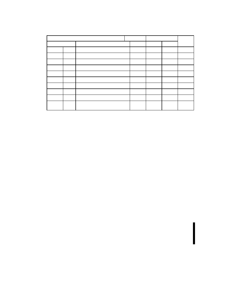
28F008SA
E
30
PRELIMINARY
9.8
AC Characteristics--Read-Only Operations
(1)
--
Extended Temperature Operation
Versions
V
CC
Ī 10%
28F008SA≠100
(5)
Unit
Symbol
Parameter
Notes
Min
Max
t
AVAV
t
RC
Read Cycle Time
100
ns
t
AVQV
t
ACC
Address to Output Delay
100
ns
t
ELQV
t
CE
CE# to Output Delay
2
100
ns
t
PHQV
t
PWH
RP# High to Output Delay
400
ns
t
GLQV
t
OE
OE# to Output Delay
2
55
ns
t
ELQX
t
LZ
CE# to Output Low Z
3
0
ns
t
EHQZ
t
HZ
CE# High to Output High Z
3
55
ns
t
GLQX
t
OLZ
OE# to Output Low Z
3
0
ns
t
GHQZ
t
DF
OE# High to Output High Z
3
30
ns
t
OH
Output Hold from Addresses, CE#
or OE# Change, Whichever is First
3
0
ns
NOTES:
1.
See AC Input/Output Reference Waveform for timing measurements.
2.
OE# may be delayed up to t
CE
≠t
OE
after the falling edge of CE# without impact on t
CE
.
3.
Sampled, not 100% tested.
4.
See High Speed AC Input/Output Reference Waveforms and High Speed AC Testing Load Circuits for testing
characteristics.
5.
See AC Input/Output Reference Waveforms and AC Testing Load Circuits for testing characteristics.
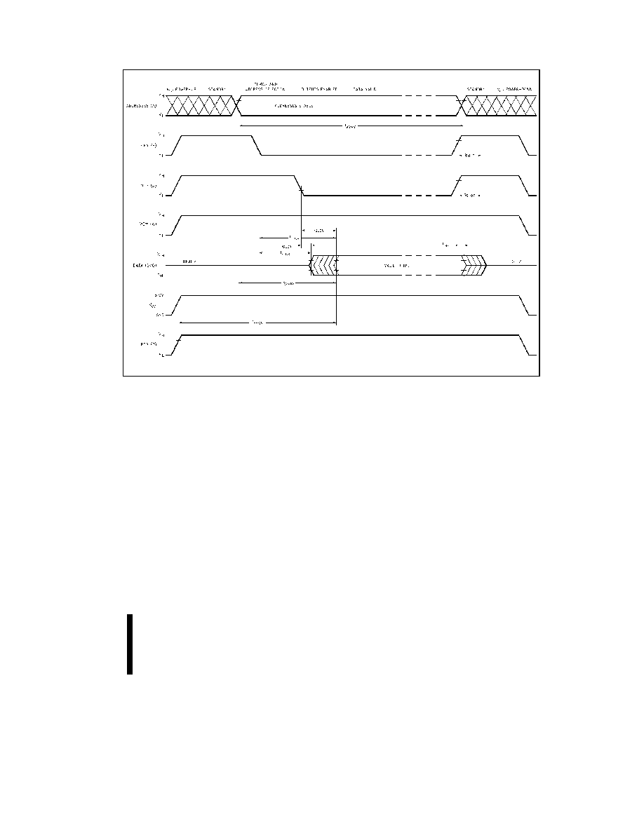
E
28F008SA
31
PRELIMINARY
29042913
Figure 13. AC Waveform for Read Operations
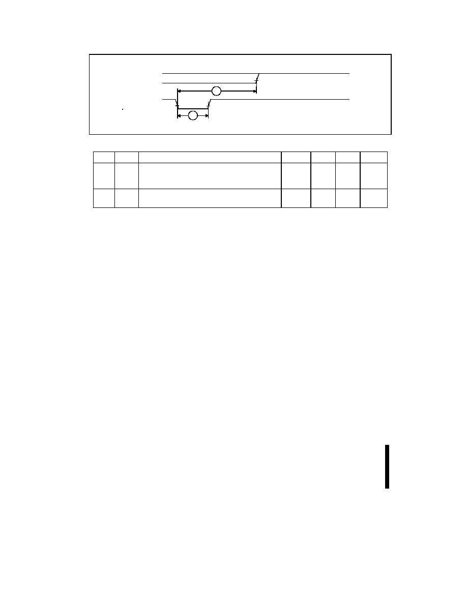
28F008SA
E
32
PRELIMINARY
IH
V
IL
V
RP# (P)
IH
V
IL
V
RY/BY# (R)
P1
P2
Figure 14. AC Waveform for Reset Operation
#
Sym
Parameter
Notes
Min
Max
Unit
P1
t
PLPH
RP# Pulse Low Time
(If RP# is tied to V
CC
, this specification is not
applicable)
100
ns
P2
t
PLRH
RP# Low to Reset during Block Erase, Program,
or Lock-Bit Configuration
2, 3
12
Ķs
NOTES:
1.
These specifications are valid for all product versions (packages and speeds).
2.
If RP# is asserted when the WSM is not busy (RY/BY# = "1"), the reset will complete within 100 ns.
3.
A reset time, t
PHQV
, is required from the latter of RY/BY# or RP# going high until outputs are valid.

E
28F008SA
33
PRELIMINARY
9.9
AC Characteristics--Write Operations
(1)
Versions
V
CC
Ī5%
28F008SA≠
85
(7)
--
--
V
CC
Ī10%
--
28F008SA≠
85
(8)
28F008SA≠
120
(8)
Unit
Symbol
Parameter
Notes
Min
Max
Min
Max
Min
Max
t
AVAV
t
WC
Write Cycle Time
85
90
120
ns
t
PHWL
t
PS
RP# High
Recovery to WE#
Going Low
2
1
1
1
Ķs
t
ELWL
t
CS
CE# Setup to
WE# Going Low
10
10
10
ns
t
WLWH
t
WP
WE# Pulse Width
40
40
40
ns
t
VPWH
t
VPS
V
PP
Setup to
WE# Going High
2
100
100
100
ns
t
AVWH
t
AS
Address Setup to
WE# Going High
3
40
40
40
ns
t
DVWH
t
DS
Data Setup to
WE# Going High
4
40
40
40
ns
t
WHDX
t
DH
Data Hold from
WE# High
5
5
5
ns
t
WHAX
t
AH
Address Hold
from WE# High
5
5
5
ns
t
WHEH
t
CH
CE# Hold from
WE# High
10
10
10
ns
t
WHWL
t
WPH
WE# Pulse Width
High
30
30
30
ns
t
WHRL
WE# High to
RY/BY# Going
Low
100
100
100
ns
t
WHQV1
Duration of Byte
Write Operation
5, 6
6
6
6
Ķs
t
WHQV2
Duration of Block
Erase Operation
5, 6
0.3
0.3
0.3
sec
t
WHGL
Write Recovery
before Read
0
0
0
Ķs
t
QVVL
t
VPH
V
PP
Hold from
Valid SRD,
RY/BY# High
2, 6
0
0
0
ns
28F008SA
E
34
PRELIMINARY
NOTES:
1.
Read timing characteristics during erase and byte write operations are the same as during read-only operations. Refer to
AC Characteristics--Read-Only Operations.
2.
Sampled, not 100% tested.
3.
Refer to Table 3 for valid A
IN
for byte write or block erasure.
4.
Refer to Table 3 for valid D
IN
for byte write or block erasure.
5.
The on-chip Write State Machine incorporates all byte write and block erase system functions and overhead of standard
Intel flash memory, including byte program and verify (byte write) and block precondition, precondition verify, erase and
erase verify (block erase).
6.
Byte write and block erase durations are measured to completion (SR.7 = 1, RY/BY# = V
OH
). V
PP
should be held at V
PPH
until determination of byte write/block erase success (SR.3/4/5 = 0)
7.
See High Speed AC Input/Output Reference Waveforms and High Speed AC Testing Load Circuits for testing
characteristics.
8.
See AC Input/Output Reference Waveforms and AC Testing Load Circuits for testing characteristics.
9.10
Block Erase and Byte Write Performance
Parameter
Notes
28F008SA-85
28F008SA-120
Unit
Typ
(1)
Max
Typ
(1)
Max
Block Erase Time
2
1.6
10
1.6
10
sec
Block Write Time
2
0.6
2.1
0.6
2.1
sec
Byte Write Time
8
(Note 3)
8
(Note 3)
Ķs
NOTES:
1. 25 įC, 12.0 V V
PP
.
2. Excludes System-Level Overhead.
3. Contact your Intel representative for information on the maximum byte write specification.
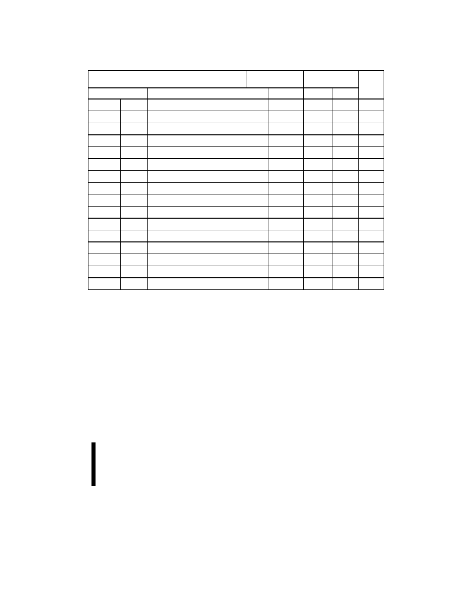
E
28F008SA
35
PRELIMINARY
9.11
AC Characteristics--Write Operations
(1)
--
Extended Temperature Operation
Versions
V
CC
Ī 10%
28F008SA≠
100
(8)
Unit
Symbol
Parameter
Notes
Min
Max
t
AVAV
t
WC
Write Cycle Time
100
ns
t
PHWL
t
PS
RP# High Recovery to WE# Going Low
2
1
Ķs
t
ELWL
t
CS
CE# Setup to WE# Going Low
10
ns
t
WLWH
t
WP
WE# Pulse Width
40
ns
t
VPWH
t
VPS
V
PP
Setup to WE# Going High
2
100
ns
t
AVWH
t
AS
Address Setup to WE# Going High
3
40
ns
t
DVWH
t
DS
Data Setup to WE# Going High
4
40
ns
t
WHDX
t
DH
Data Hold from WE# High
5
ns
t
WHAX
t
AH
Address Hold from WE# High
5
ns
t
WHEH
t
CH
CE# Hold from WE# High
10
ns
t
WHWL
t
WPH
WE# Pulse Width High
30
ns
t
WHRL
WE# High to RY/BY# Going Low
100
ns
t
WHQV1
Duration of Byte Write Operation
5, 6
6
Ķs
t
WHQV2
Duration of Block Erase Operation
5, 6
0.3
sec
t
WHGL
Write Recovery before Read
0
Ķs
t
QVVL
t
VPH
V
PP
Hold from Valid SRD, RY/BY# High
2, 6
0
ns
NOTES:
1.
Read timing characteristics during erase and byte write operations are the same as during read-only operations. Refer to
AC Characteristics--Read-Only Operations.
2.
Sampled, not 100% tested.
3.
Refer to Table 3 for valid A
IN
for byte write or block erasure.
4.
Refer to Table 3 for valid D
IN
for byte write or block erasure.
5.
The on-chip WSM incorporates all byte write and block erase system functions and overhead of standard Intel flash
memory, including byte program and verify (byte write) and block precondition, precondition verify, erase and erase verify
(block erase).
6.
Byte write and block erase durations are measured to completion (SR.7 = 1, RY/BY# = V
OH
). V
PP
should be held at V
PPH
until determination of byte write/block erase success (SR.3/4/5 = 0)
7.
See High Speed AC Input/Output Reference Waveforms and High Speed AC Testing Load Circuits for testing
characteristics.
8.
See AC Input/Output Reference Waveforms and AC Testing Load Circuits for testing characteristics.

28F008SA
E
36
PRELIMINARY
9.12
Block Erase and Byte Write Performance--
Extended Temperature Operation
Parameter
Notes
28F008SA-100
Unit
Typ
(1)
Max
Block Erase Time
2
1.6
10
sec
Block Write Time
2
0.6
2.1
sec
Byte Write Time
8
(Note 3)
Ķs
NOTES:
1.
25 įC, 12.0 V V
PP
.
2.
Excludes System-Level Overhead.
3.
Contact your Intel representative for information on the maximum byte write specification.

E
28F008SA
37
PRELIMINARY
29042914
Figure 15. AC Waveform for Write Operations

28F008SA
E
38
PRELIMINARY
9.13
Alternative CE#-Controlled Writes
Versions
V
CC
Ī5%
28F008SA≠
85
(6)
--
--
V
CC
Ī10%
--
28F008SA≠
85
(7)
28F008SA≠
120
(7)
Unit
Sym
Parameter
Notes
Min
Max
Min
Max
Min
Max
t
AVAV
t
WC
Write Cycle Time
85
90
120
ns
t
PHEL
t
PS
RP# High
Recovery to CE#
Going Low
2
1
1
1
Ķs
t
WLEL
t
WS
WE# Setup to
CE# Going Low
0
0
0
ns
t
ELEH
t
CP
CE# Pulse Width
50
50
50
ns
t
VPEH
t
VPS
V
PP
Setup to CE#
Going High
2
100
100
100
ns
t
AVEH
t
AS
Address Setup to
CE# Going High
3
40
40
40
ns
t
DVEH
t
DS
Data Setup to
CE# Going High
4
40
40
40
ns
t
EHDX
t
DH
Data Hold from
CE# High
5
5
5
ns
t
EHAX
t
AH
Address Hold
from CE# High
5
5
5
ns
t
EHWH
t
WH
WE# Hold from
CE# High
0
0
0
ns
t
EHEL
t
EPH
CE# Pulse Width
High
25
25
25
ns
t
EHRL
CE# High to
RY/BY# Going
Low
100
100
100
ns
t
EHQV
1
Duration of Byte
Write Operation
5
6
6
6
Ķs
t
EHQV
2
Duration of Block
Erase Operation
5
0.3
0.3
0.3
sec
t
EHGL
Write Recovery
before Read
0
0
0
Ķs
t
QVVL
t
VPH
V
PP
Hold from
Valid SRD,
RY/BY# High
2, 5
0
0
0
ns

E
28F008SA
39
PRELIMINARY
NOTES:
1.
Chip-Enable Controlled Writes: Write operations are driven by the valid combination of CE# and WE#. In systems where
CE# defines the write pulsewidth (within a longer WE# timing waveform), all setup, hold and inactive WE# times should be
measured relative to the CE# waveform.
2.
Sampled, not 100% tested.
3.
Refer to Table 3 for valid A
IN
for byte write or block erasure.
4.
Refer to Table 3 for valid D
IN
for byte write or block erasure.
5.
Byte write and block erase durations are measured to completion (SR.7 = 1, RY/BY# = V
OH
). V
PP
should be held at V
PPH
until determination of byte write/block erase success (SR.3/4/5 = 0)
6.
See High Speed AC Input/Output Reference Waveforms and High Speed AC Testing Load Circuits for testing
characteristics.
7.
See AC Input/Output Reference Waveforms and AC Testing Load Circuits for testing characteristics.
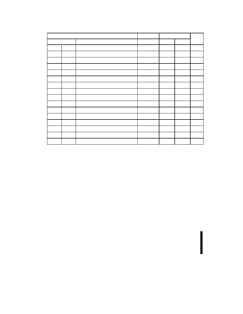
28F008SA
E
40
PRELIMINARY
9.14
Alternative CE#-Controlled Writes-- Extended Temperature Operation
Versions
V
CC
Ī10%
28F008SA-100
(7)
Symbol
Parameter
Notes
Min
Max
Unit
t
AVAV
t
WC
Write Cycle Time
100
ns
t
PHEL
t
PS
RP# High Recovery to CE# Going Low
2
1
Ķs
t
WLEL
t
WS
WE# Setup to CE# Going Low
0
ns
t
ELEH
t
CP
CE# Pulse Width
50
ns
t
VPEH
t
VPS
V
PP
Setup to CE# Going High
2
100
ns
t
AVEH
t
AS
Address Setup to CE# Going High
3
40
ns
t
DVEH
t
DS
Data Setup to CE# Going High
4
40
ns
t
EHDX
t
DH
Data Hold from CE# High
5
ns
t
EHAX
t
AH
Address Hold from CE# High
5
ns
t
EHWH
t
WH
WE# Hold from CE# High
0
ns
t
EHEL
t
EPH
CE# Pulse Width High
25
ns
t
EHRL
CE# High to RY/BY# Going Low
100
ns
t
EHQV1
Duration of Byte Write Operation
5
6
Ķs
t
EHQV2
Duration of Block Erase Operation
5
0.3
sec
t
EHGL
Write Recovery before Read
0
Ķs
t
QVVL
t
VPH
V
PP
Hold from Valid SRD, RY/BY# High
2, 5
0
ns
NOTES:
1.
Chip-Enable Controlled Writes: Write operations are driven by the valid combination of CE# and WE#. In systems where
CE# defines the write pulsewidth (within a longer WE# timing waveform), all setup, hold and inactive WE# times should be
measured relative to the CE# waveform.
2.
Sampled, not 100% tested.
3.
Refer to Table 3 for valid A
IN
for byte write or block erasure.
4.
Refer to Table 3 for valid D
IN
for byte write or block erasure.
5.
Byte write and block erase durations are measured to completion (SR.7 = 1, RY/BY# = V
OH
). V
PP
should be held at V
PPH
until determination of byte write/block erase success (SR.3/4/5 = 0)
6.
See High Speed AC Input/Output Reference Waveforms and High Speed AC Testing Load Circuits for testing
characteristics.
7.
See AC Input/Output Reference Waveforms and AC Testing Load Circuits for testing characteristics.
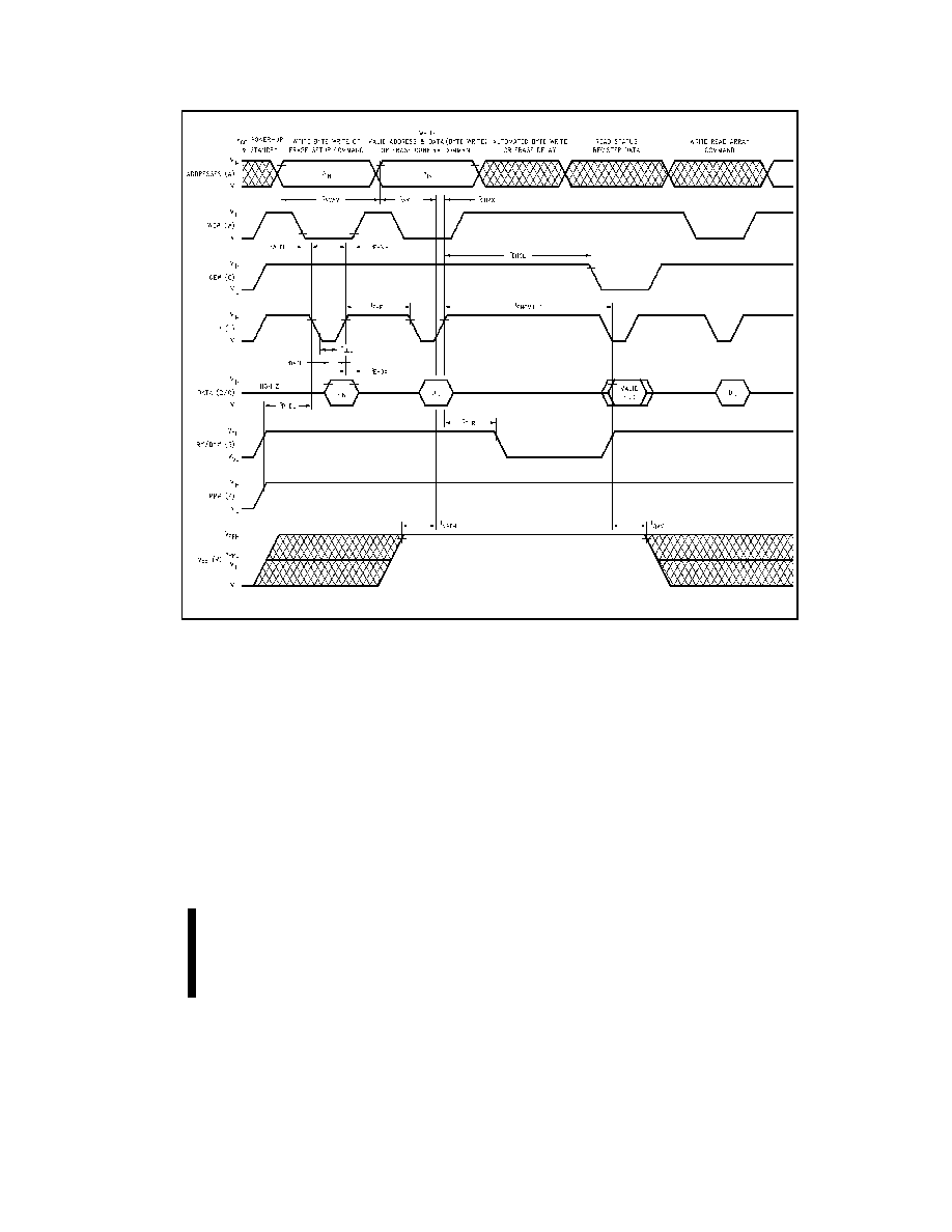
E
28F008SA
41
PRELIMINARY
29042915
Figure 16. Alternate AC Waveform for Write Operations
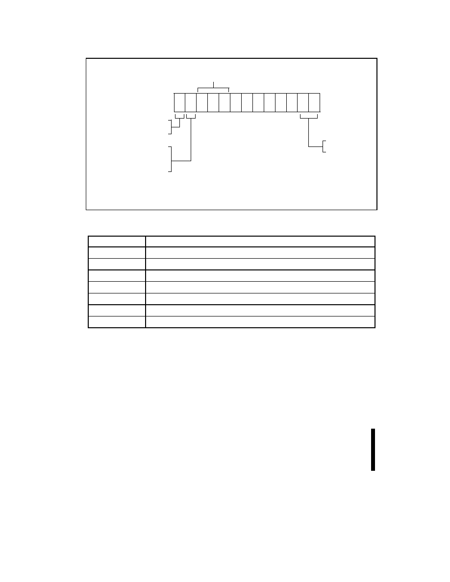
28F008SA
E
42
PRELIMINARY
10.0 ORDERING INFORMATION
E 2 8 F 0 0 8 S A - 8
Operating Temperature
T = Extended Temp
Blank = Commercial Temp
Access Speed (ns)
85, 120
Package
E = Standard 40-Lead TSOP
PA = 44=-Lead PSOP
TB = 44-Lead PSOP (Ext. Temp.)
Product Line Designator for all Intel
ģ
Flash products
5
VALID COMBINATIONS
E28F008SA-85
PA28F008SA-85
TE28F008SA-100
TB28F008SA-100
E28F008SA-120
PA28F008SA-120
TF28F008SA-100
11.0 ADDITIONAL INFORMATION
Order Number
Document/Tool
290597
5 Volt FlashFileTM Memory; 28F004S5, 28F008S5, 28F016S5 datasheet
290598
3 Volt FlashFileTM Memory; 28F004S3, 28F008S3, 28F016S3 datasheet
271296
28F008SA 8-Mbit (1-Mbit x 8) Flash Memory SmartDieTM Product Specification
292180
AP-625 28F008SC Compatibility with 28F008SA
297183
28F008 SA/SA-L Specification Update
Note 3
AP-359 28F008SA Hardware Interfacing
Note 3
AP-364 28F008SA Automation and Algorithms
NOTES:
1.
Please call the Intel Literature Center at (800) 548-4725 to request Intel documentation. International customers should
contact their local Intel or distribution sales office.
2.
Visit Intel's World Wide Web home page at http://www.intel.com for technical documentation and tools.
3.
These documents can be located at the Intel World Wide Web support site, http://www.intel.com/support/flash/memory