Other brands and names are the property of their respective owners
Information in this document is provided in connection with Intel products Intel assumes no liability whatsoever including infringement of any patent or
copyright for sale and use of Intel products except as provided in Intel's Terms and Conditions of Sale for such products Intel retains the right to make
changes to these specifications at any time without notice Microcomputer Products may have minor variations to this specification known as errata
January 1994
COPYRIGHT
INTEL CORPORATION 1995
Order Number 240187-008
Intel386
TM
SX MICROPROCESSOR
Y
Full 32-Bit Internal Architecture
8- 16- 32-Bit Data Types
8 General Purpose 32-Bit Registers
Y
Runs Intel386
TM
Software in a Cost
Effective 16-Bit Hardware Environment
Runs Same Applications and O S 's
as the Intel386
TM
DX Processor
Object Code Compatible with 8086
80186 80286 and Intel386
TM
Processors
Y
High Performance 16-Bit Data Bus
16 20 25 and 33 MHz Clock
Two-Clock Bus Cycles
Address Pipelining Allows Use of
Slower Cheaper Memories
Y
Integrated Memory Management Unit
Virtual Memory Support
Optional On-Chip Paging
4 Levels of Hardware Enforced
Protection
MMU Fully Compatible with Those of
the 80286 and Intel386 DX CPUs
Y
Virtual 8086 Mode Allows Execution of
8086 Software in a Protected and
Paged System
Y
Large Uniform Address Space
16 Megabyte Physical
64 Terabyte Virtual
4 Gigabyte Maximum Segment Size
Y
Numerics Support with the Intel387
TM
SX Math CoProcessor
Y
On-Chip Debugging Support Including
Breakpoint Registers
Y
Complete System Development
Support
Software C PL M Assembler
Debuggers PMON-386 DX
ICE
TM
-386 SX
Y
High Speed CHMOS IV Technology
Y
Operating Frequency
Standard
(Intel386 SX -33 -25 -20 -16)
Min Max Frequency
(4 33 4 25 4 20 4 16) MHz
Low Power
(Intel386 SX -33 -25 -20 -16 -12)
Min Max Frequency
(2 33 2 25 2 20 2 16 2 12) MHz
Y
100-Pin Plastic Quad Flatpack Package
(See Packaging Outlines and Dimensions
231369)
The Intel386
TM
SX Microprocessor is an entry-level 32-bit CPU with a 16-bit external data bus and a 24-bit
external address bus The Intel386 SX CPU brings the vast software library of the Intel386
TM
Architecture to
entry-level systems It provides the performance benefits of a 32-bit programming architecture with the cost
savings associated with 16-bit hardware systems
240187 � 47
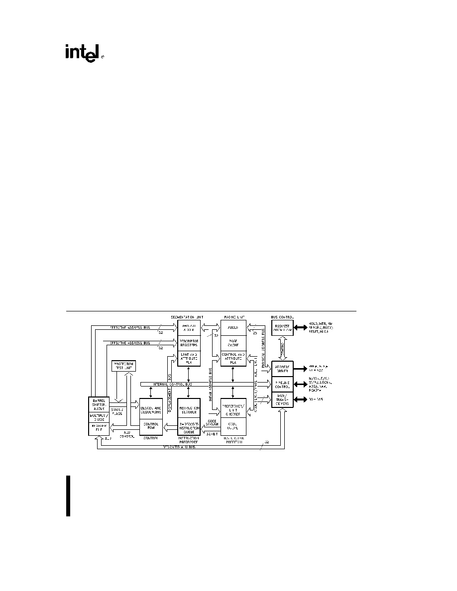
Intel386
TM
SX Pipelined 32-Bit Microarchitecture

Intel386
TM
SX MICROPROCESSOR
Intel386
TM
SX MicroProcessor
CONTENTS
PAGE
1 0 PIN DESCRIPTION
3
2 0 BASE ARCHITECTURE
6
2 1 Register Set
6
2 2 Instruction Set
10
2 3 Memory Organization
11
2 4 Addressing Modes
12
2 5 Data Types
15
2 6 I O Space
15
2 7 Interrupts and Exceptions
17
2 8 Reset and Initialization
20
2 9 Testability
20
2 10 Debugging Support
21
3 0 REAL MODE ARCHITECTURE
22
3 1 Memory Addressing
22
3 2 Reserved Locations
23
3 3 Interrupts
23
3 4 Shutdown and Halt
23
3 5 LOCK Operations
23
4 0 PROTECTED MODE
ARCHITECTURE
24
4 1 Addressing Mechanism
24
4 2 Segmentation
24
4 3 Protection
29
4 4 Paging
33
4 5 Virtual 8086 Environment
36
CONTENTS
PAGE
5 0 FUNCTIONAL DATA
39
5 1 Signal Description Overview
39
5 2 Bus Transfer Mechanism
45
5 3 Memory and I O Spaces
45
5 4 Bus Functional Description
45
5 5 Self-test Signature
63
5 6 Component and Revision
Identifiers
63
5 7 Coprocessor Interfacing
63
6 0 PACKAGE THERMAL
SPECIFICATIONS
64
7 0 ELECTRICAL SPECIFICATIONS
64
7 1 Power and Grounding
64
7 2 Maximum Ratings
65
7 3 D C Specifications
66
7 4 A C Specifications
68
7 5 Designing for ICE
TM
-Intel386 SX
Emulator
78
8 0 DIFFERENCES BETWEEN THE
Intel386
TM
SX CPU and the
Intel386
TM
DX CPU
79
9 0 INSTRUCTION SET
80
9 1 Intel386
TM
SX CPU Instruction
Encoding and Clock Count Summary
80
9 2 Instruction Encoding
95
2

Intel386
TM
SX MICROPROCESSOR
1 0 PIN DESCRIPTION
240187 � 1
NOTE
NC
e
No Connect
Figure 1 1 Intel386
TM
SX Microprocessor Pin out Top View
Table 1 1 Alphabetical Pin Assignments
Address
Data
Control
N C
V
CC
V
SS
A
1
18
D
0
1
ADS
16
20
8
2
A
2
51
D
1
100
BHE
19
27
9
5
A
3
52
D
2
99
BLE
17
29
10
11
A
4
53
D
3
96
BUSY
34
30
21
12
A
5
54
D
4
95
CLK2
15
31
32
13
A
6
55
D
5
94
D C
24
43
39
14
A
7
56
D
6
93
ERROR
36
44
42
22
A
8
58
D
7
92
FLT
28
45
48
35
A
9
59
D
8
90
HLDA
3
46
57
41
A
10
60
D
9
89
HOLD
4
47
69
49
A
11
61
D
10
88
INTR
40
71
50
A
12
62
D
11
87
LOCK
26
84
63
A
13
64
D
12
86
M IO
23
91
67
A
14
65
D
13
83
NA
6
97
68
A
15
66
D
14
82
NMI
38
77
A
16
70
D
15
81
PEREQ
37
78
A
17
72
READY
7
85
A
18
73
RESET
33
98
A
19
74
W R
25
A
20
75
A
21
76
A
22
79
A
23
80
3

Intel386
TM
SX MICROPROCESSOR
1 0 PIN DESCRIPTION
(Continued)
The following are the Intel386
TM
SX Microprocessor pin descriptions The following definitions are used in the
pin descriptions
The named signal is active LOW
I
Input signal
O
Output signal
I O
Input and Output signal
-
No electrical connection
Symbol
Type
Pin
Name and Function
CLK2
I
15
CLK2
provides the fundamental timing for the Intel386 SX
Microprocessor For additional information see Clock
RESET
I
33
RESET
suspends any operation in progress and places the
Intel386 SX Microprocessor in a known reset state See
Interrupt Signals
for additional information
D
15
� D
0
I O
81-83 86-90
Data Bus
inputs data during memory I O and interrupt
acknowledge read cycles and outputs data during memory and
92-96 99-100 1
I O write cycles See Data Bus for additional information
A
23
� A
1
O
80-79 76-72 70
Address Bus
outputs physical memory or port I O addresses
See Address Bus for additional information
66-64 62-58
56-51 18
W R
O
25
Write Read
is a bus cycle definition pin that distinguishes write
cycles from read cycles See Bus Cycle Definition Signals for
additional information
D C
O
24
Data Control
is a bus cycle definition pin that distinguishes data
cycles either memory or I O from control cycles which are
interrupt acknowledge halt and code fetch See Bus Cycle
Definition Signals
for additional information
M IO
O
23
Memory IO
is a bus cycle definition pin that distinguishes
memory cycles from input output cycles See Bus Cycle
Definition Signals
for additional information
LOCK
O
26
Bus Lock
is a bus cycle definition pin that indicates that other
system bus masters are not to gain control of the system bus
while it is active See Bus Cycle Definition Signals for
additional information
ADS
O
16
Address Status
indicates that a valid bus cycle definition and
address (W R
D C
M IO
BHE
BLE
and A
23
� A
1
are
being driven at the Intel386 SX Microprocessor pins See Bus
Control Signals
for additional information
NA
I
6
Next Address
is used to request address pipelining See Bus
Control Signals
for additional information
READY
I
7
Bus Ready
terminates the bus cycle See Bus Control Signals
for additional information
BHE
BLE
O
19 17
Byte Enables
indicate which data bytes of the data bus take part
in a bus cycle See Address Bus for additional information
4

Intel386
TM
SX MICROPROCESSOR
1 0 PIN DESCRIPTION
(Continued)
Symbol
Type
Pin
Name and Function
HOLD
I
4
Bus Hold Request
input allows another bus master to request
control of the local bus See Bus Arbitration Signals for
additional information
HLDA
O
3
Bus Hold Acknowledge
output indicates that the Intel386 SX
Microprocessor has surrendered control of its local bus to
another bus master See Bus Arbitration Signals for additional
information
INTR
I
40
Interrupt Request
is a maskable input that signals the Intel386
SX Microprocessor to suspend execution of the current program
and execute an interrupt acknowledge function See Interrupt
Signals
for additional information
NMI
I
38
Non-Maskable Interrupt Request
is a non-maskable input that
signals the Intel386 SX Microprocessor to suspend execution of
the current program and execute an interrupt acknowledge
function See Interrupt Signals for additional information
BUSY
I
34
Busy
signals a busy condition from a processor extension See
Coprocessor Interface Signals
for additional information
ERROR
I
36
Error
signals an error condition from a processor extension See
Coprocessor Interface Signals
for additional information
PEREQ
I
37
Processor Extension Request
indicates that the processor has
data to be transferred by the Intel386 SX Microprocessor See
Coprocessor Interface Signals
for additional information
FLT
I
28
Float
is an input which forces all bidirectional and output signals
including HLDA to the tri-state condition This allows the
electrically isolated Intel386SX PQFP to use ONCE (On-Circuit
Emulation) method without removing it from the PCB See Float
for additional information
N C
-
20 27 29-31 43-47
No Connects
should always be left unconnected Connection of
a N C pin may cause the processor to malfunction or be
incompatible with future steppings of the Intel386 SX
Microprocessor
V
CC
I
8-10 21 32 39
System Power
provides the a5V nominal DC supply input
42 48 57 69
71 84 91 97
V
SS
I
2 5 11-14 22
System Ground
provides the 0V connection from which all
inputs and outputs are measured
35 41 49-50
63 67-68
77-78 85 98
5

Intel386
TM
SX MICROPROCESSOR
INTRODUCTION
The Intel386 SX Microprocessor is 100% object
code compatible with the Intel386 DX 286 and 8086
microprocessors Systems based on the Intel386 SX
CPU can access the world's largest existing micro-
computer software base including the growing 32-
bit software base
Instruction pipelining and a high performance ALU
ensure short average instruction execution times
and high system throughput
The integrated memory management unit (MMU) in-
cludes an address translation cache multi-tasking
hardware and a four-level hardware-enforced pro-
tection mechanism to support operating systems
The virtual machine capability of the Intel386 SX
CPU allows simultaneous execution of applications
from multiple operating systems
The Intel386 SX CPU offers on-chip testability and
debugging features Four breakpoint registers allow
conditional or unconditional breakpoint traps on
code execution or data accesses for powerful de-
bugging of even ROM-based systems Other testa-
bility features include self-test tri-state of output
buffers and direct access to the page translation
cache
The Low Power Intel386 SX CPU brings the benefits
of the Intel386 Microprocessor 32-bit architecture to
Laptop and Notebook personal computer applica-
tions With its power saving 2 MHz sleep-mode and
extended functional temperature range of 0 C to
100 C T
CASE
the Lower Power Intel386 SX CPU
specifically satisfies the power consumption and
heat dissipation requirements of today's small form
factor computers
2 0 BASE ARCHITECTURE
The Intel386 SX Microprocessor consists of a cen-
tral processing unit a memory management unit and
a bus interface
The central processing unit consists of the execu-
tion unit and the instruction unit The execution unit
contains the eight 32-bit general purpose registers
which are used for both address calculation and
data operations and a 64-bit barrel shifter used to
speed shift rotate multiply and divide operations
The instruction unit decodes the instruction opcodes
and stores them in the decoded instruction queue
for immediate use by the execution unit
The memory management unit (MMU) consists of a
segmentation unit and a paging unit Segmentation
allows the managing of the logical address space by
providing an extra addressing component one that
allows easy code and data relocatability and effi-
cient sharing The paging mechanism operates be-
neath and is transparent to the segmentation pro-
cess to allow management of the physical address
space
The segmentation unit provides four levels of pro-
tection for isolating and protecting applications and
the operating system from each other The hardware
enforced protection allows the design of systems
with a high degree of integrity
The Intel386 SX Microprocessor has two modes of
operation Real Address Mode (Real Mode) and
Protected Virtual Address Mode (Protected Mode)
In Real Mode the Intel386 SX Microprocessor oper-
ates as a very fast 8086 but with 32-bit extensions if
desired Real Mode is required primarily to set up the
processor for Protected Mode operation
Within Protected Mode software can perform a task
switch to enter into tasks designated as Virtual 8086
Mode tasks Each such task behaves with 8086 se-
mantics thus allowing 8086 software (an application
program or an entire operating system) to execute
The Virtual 8086 tasks can be isolated and protect-
ed from one another and the host Intel386 SX Micro-
processor operating system by use of paging
Finally to facilitate system hardware designs the
Intel386 SX Microprocessor bus interface offers ad-
dress pipelining and direct Byte Enable signals for
each byte of the data bus
2 1 Register Set
The Intel386 SX Microprocessor has thirty-four reg-
isters as shown in Figure 2-1 These registers are
grouped into the following seven categories
General Purpose Registers
The eight 32-bit gen-
eral purpose registers are used to contain arithmetic
and logical operands Four of these (EAX EBX
ECX and EDX) can be used either in their entirety as
32-bit registers as 16-bit registers or split into pairs
of separate 8-bit registers
6

Intel386
TM
SX MICROPROCESSOR
240187 � 2
Figure 2 1 Intel386
TM
SX Microprocessor Registers
7

Intel386
TM
SX MICROPROCESSOR
Segment Registers
Six 16-bit special purpose reg-
isters select at any given time the segments of
memory that are immediately addressable for code
stack and data
Flags and Instruction Pointer Registers
The two
32-bit special purpose registers in figure 2 1 record
or control certain aspects of the Intel386 SX Micro-
processor state
The EFLAGS register includes
status and control bits that are used to reflect the
outcome of many instructions and modify the se-
mantics of some instructions The Instruction Point-
er called EIP is 32 bits wide The Instruction Pointer
controls instruction fetching and the processor auto-
matically increments it after executing an instruction
Control Registers
The four 32-bit control register
are used to control the global nature of the Intel386
SX Microprocessor The CR0 register contains bits
that set the different processor modes (Protected
Real Paging and Coprocessor Emulation) CR2 and
CR3 registers are used in the paging operation
System Address Registers
These four special
registers reference the tables or segments support-
ed by the 80286 Intel386 SX Intel386 DX CPU's
protection model These tables or segments are
GDTR (Global Descriptor Table Register)
IDTR (Interrupt Descriptor Table Register)
LDTR (Local Descriptor Table Register)
TR (Task State Segment Register)
Debug Registers
The six programmer accessible
debug registers provide on-chip support for debug-
ging The use of the debug registers is described in
Section 2 10 Debugging Support
Test Registers
Two registers are used to control
the testing of the RAM CAM (Content Addressable
Memories) in the Translation Lookaside Buffer por-
tion of the Intel386 SX Microprocessor Their use is
discussed in Testability
240187 � 3
Figure 2 2 Status and Control Register Bit Functions
8

Intel386
TM
SX MICROPROCESSOR
EFLAGS REGISTER
The flag register is a 32-bit register named EFLAGS
The defined bits and bit fields within EFLAGS
shown in Figure 2 2 control certain operations and
indicate the status of the Intel386 SX Microproces-
sor The lower 16 bits (bits 0 � 15) of EFLAGS con-
tain the 16-bit flag register named FLAGS This is
the default flag register used when executing 8086
80286 or real mode code The functions of the flag
bits are given in Table 2 1
CONTROL REGISTERS
The Intel386 SX Microprocessor has three control
registers of 32 bits CR0 CR2 and CR3 to hold the
machine state of a global nature These registers
are shown in Figures 2 1 and 2 2 The defined CR0
bits are described in Table 2 2
Table 2 1 Flag Definitions
Bit Position
Name
Function
0
CF
Carry Flag
Set on high-order bit carry or borrow cleared
otherwise
2
PF
Parity Flag
Set if low-order 8 bits of result contain an even
number of 1-bits cleared otherwise
4
AF
Auxiliary Carry Flag
Set on carry from or borrow to the low
order four bits of AL cleared otherwise
6
ZF
Zero Flag
Set if result is zero cleared otherwise
7
SF
Sign Flag
Set equal to high-order bit of result (0 if positive 1 if
negative)
8
TF
Single Step Flag
Once set a single step interrupt occurs after
the next instruction executes TF is cleared by the single step
interrupt
9
IF
Interrupt-Enable Flag
When set maskable interrupts will cause
the CPU to transfer control to an interrupt vector specified
location
10
DF
Direction Flag
Causes string instructions to auto-increment
(default) the appropriate index registers when cleared Setting
DF causes auto-decrement
11
OF
Overflow Flag
Set if the operation resulted in a carry borrow
into the sign bit (high-order bit) of the result but did not result in a
carry borrow out of the high-order bit or vice-versa
12 13
IOPL
I O Privilege Level
Indicates the maximum Current Privilege
Level (CPL) permitted to execute I O instructions without
generating an exception 13 fault or consulting the I O permission
bit map while executing in protected mode For virtual 86 mode it
indicates the maximum CPL allowing alteration of the IF bit See
Section 4 2 for a further discussion and definitions on various
privilege levels
14
NT
Nested Task
Set if the execution of the current task is nested
within another task Cleared otherwise
16
RF
Resume Flag
Used in conjunction with debug register
breakpoints It is checked at instruction boundaries before
breakpoint processing If set any debug fault is ignored on the
next instruction
17
VM
Virtual 8086 Mode
If set while in protected mode the Intel386
SX Microprocessor will switch to virtual 8086 operation handling
segment loads as the 8086 does but generating exception 13
faults on privileged opcodes
9

Intel386
TM
SX MICROPROCESSOR
Table 2 2 CR0 Definitions
Bit Position
Name
Function
0
PE
Protection mode enable
places the Intel386 SX Microprocessor
into protected mode If PE is reset the processor operates again
in Real Mode PE may be set by loading MSW or CR0 PE can be
reset only by loading CR0 it cannot be reset by the LMSW
instruction
1
MP
Monitor coprocessor extension
allows WAIT instructions to
cause a processor extension not present exception (number 7)
2
EM
Emulate processor extension
causes a processor extension
not present exception (number 7) on ESC instructions to allow
emulating a processor extension
3
TS
Task switched
indicates the next instruction using a processor
extension will cause exception 7 allowing software to test
whether the current processor extension context belongs to the
current task
31
PG
Paging enable bit
is set to enable the on-chip paging unit It is
reset to disable the on-chip paging unit
2 2 Instruction Set
The instruction set is divided into nine categories of
operations
Data Transfer
Arithmetic
Shift Rotate
String Manipulation
Bit Manipulation
Control Transfer
High Level Language Support
Operating System Support
Processor Control
These instructions are listed in Table 9 1 Instruc-
tion Set Clock Count Summary
All Intel386 SX Microprocessor instructions operate
on either 0 1 2 or 3 operands an operand resides
in a register in the instruction itself or in memory
Most zero operand instructions (e g CLI STI) take
only one byte One operand instructions generally
are two bytes long The average instruction is 3 2
bytes long Since the Intel386 SX Microprocessor
has a 16 byte prefetch instruction queue an average
of 5 instructions will be prefetched The use of two
operands permits the following types of common in-
structions
Register to Register
Memory to Register
Immediate to Register
Memory to Memory
Register to Memory
Immediate to Memory
The operands can be either 8 16 or 32 bits long As
a general rule when executing code written for the
Intel386 SX Microprocessor (32-bit code) operands
are 8 or 32 bits when executing existing 8086 or
80286 code (16-bit code) operands are 8 or 16 bits
Prefixes can be added to all instructions which over-
ride the default length of the operands (i e use
32-bit operands for 16-bit code or 16-bit operands
for 32-bit code)
10

Intel386
TM
SX MICROPROCESSOR
2 3 Memory Organization
Memory on the Intel386 SX Microprocessor is divid-
ed into 8-bit quantities (bytes)
16-bit quantities
(words) and 32-bit quantities (dwords) Words are
stored in two consecutive bytes in memory with the
low-order byte at the lowest address Dwords are
stored in four consecutive bytes in memory with the
low-order byte at the lowest address The address of
a word or dword is the byte address of the low-order
byte
In addition to these basic data types the Intel386 SX
Microprocessor supports two larger units of memory
pages and segments Memory can be divided up
into one or more variable length segments which
can be swapped to disk or shared between pro-
grams Memory can also be organized into one or
more 4K byte pages Finally both segmentation and
paging can be combined gaining the advantages of
both systems The Intel386 SX Microprocessor sup-
ports both pages and segmentation in order to pro-
vide maximum flexibility to the system designer
Segmentation and paging are complementary Seg-
mentation is useful for organizing memory in logical
modules and as such is a tool for the application
programmer while pages are useful to the system
programmer for managing the physical memory of a
system
ADDRESS SPACES
The Intel386 SX Microprocessor has three types of
address spaces logical linear and physical A
logical
address (also known as a virtual address)
consists of a selector and an offset A selector is the
contents of a segment register An offset is formed
by summing all of the addressing components
(BASE INDEX DISPLACEMENT) discussed in sec-
tion 2 4 Addressing Modes into an effective ad-
dress This effective address along with the selector
is known as the logical address Since each task on
the Intel386 SX Microprocessor has a maximum of
16K (2
14
b
1) selectors and offsets can be 4 giga-
bytes (with paging enabled) this gives a total of 2
46
bits or 64 terabytes of logical address space per
task The programmer sees the logical address
space
The segmentation unit translates the logical ad-
dress space into a 32-bit linear address space If the
paging unit is not enabled then the 32-bit linear ad-
dress is truncated into a 24-bit physical address
The physical address is what appears on the ad-
dress pins
The primary differences between Real Mode and
Protected Mode are how the segmentation unit per-
forms the translation of the logical address into the
linear
address size of the address space and pag-
ing capability In Real Mode the segmentation unit
shifts the selector left four bits and adds the result to
the effective address to form the linear address
This linear address is limited to 1 megabyte In addi-
tion real mode has no paging capability
Protected Mode will see one of two different ad-
dress spaces depending on whether or not paging
is enabled Every selector has a logical base ad-
dress associated with it that can be up to 32 bits in
length This 32-bit logical base address is added to
the effective address to form a final 32-bit linear
address If paging is disabled this final linear ad-
dress reflects physical memory and is truncated so
that only the lower 24 bits of this address are used
to address the 16 megabyte memory address space
If paging is enabled this final linear address reflects
a 32-bit address that is translated through the pag-
ing unit to form a 16-megabyte physical address
The logical base address is stored in one of two
operating system tables (i e the Local Descriptor
Table or Global Descriptor Table)
Figure 2 3 shows the relationship between the vari-
ous address spaces
11

Intel386
TM
SX MICROPROCESSOR
240187 � 4
Figure 2 3 Address Translation
SEGMENT REGISTER USAGE
The main data structure used to organize memory is
the segment On the Intel386 SX Microprocessor
segments are variable sized blocks of linear ad-
dresses which have certain attributes associated
with them There are two main types of segments
code and data The segments are of variable size
and can be as small as 1 byte or as large as 4 giga-
bytes (2
32
bits)
In order to provide compact instruction encoding
and increase processor performance instructions
do not need to explicitly specify which segment reg-
ister is used The segment register is automatically
chosen according to the rules of Table 2 3 (Segment
Register Selection Rules) In general data refer-
ences use the selector contained in the DS register
stack references use the SS register and instruction
fetches use the CS register The contents of the In-
struction Pointer provide the offset Special segment
override prefixes allow the explicit use of a given
segment register and override the implicit rules list-
ed in Table 2 3 The override prefixes also allow the
use of the ES FS and GS segment registers
There are no restrictions regarding the overlapping
of the base addresses of any segments Thus all 6
segments could have the base address set to zero
and create a system with a four gigabyte linear ad-
dress space This creates a system where the virtual
address space is the same as the linear address
space
Further details of segmentation are dis-
cussed in chapter 4 PROTECTED MODE ARCHI-
TECTURE
2 4 Addressing Modes
The Intel386 SX Microprocessor provides a total of 8
addressing modes for instructions to specify oper-
ands The addressing modes are optimized to allow
the efficient execution of high level languages such
as C and FORTRAN and they cover the vast majori-
ty of data references needed by high-level lan-
guages
REGISTER AND IMMEDIATE MODES
Two of the addressing modes provide for instruc-
tions that operate on register or immediate oper-
ands
Register Operand Mode
The operand is located in
one of the 8 16 or 32-bit general registers
Immediate Operand Mode
The operand is includ-
ed in the instruction as part of the opcode
12

Intel386
TM
SX MICROPROCESSOR
Table 2 3 Segment Register Selection Rules
Type of
Implied (Default)
Segment Override
Memory Reference
Segment Use
Prefixes Possible
Code Fetch
CS
None
Destination of PUSH PUSHF INT
CALL PUSHA Instructons
SS
None
Source of POP POPA POPF IRET
RET Instructions
SS
None
Destination of STOS MOVE REP STOS
and REP MOVS instructions
ES
None
Other data references with effective
address using base register of
EAX
DS
CS SS ES FS GS
EBX
DS
CS SS ES FS GS
ECX
DS
CS SS ES FS GS
EDX
DS
CS SS ES FS GS
ESI
DS
CS SS ES FS GS
EDI
DS
CS SS ES FS GS
EBP
SS
CS DS ES FS GS
ESP
SS
CS DS ES FS GS
32-BIT MEMORY ADDRESSING MODES
The remaining 6 modes provide a mechanism for
specifying the effective address of an operand The
linear address consists of two components the seg-
ment base address and an effective address The
effective address is calculated by summing any
combination of the following three address elements
(see Figure 2 3)
DISPLACEMENT
an 8 16 or 32-bit immediate val-
ue following the instruction
BASE
The contents of any general purpose regis-
ter The base registers are generally used by compil-
ers to point to the start of the local variable area
INDEX
The contents of any general purpose regis-
ter except for ESP The index registers are used to
access the elements of an array or a string of char-
acters The index register's value can be multiplied
by a scale factor either 1 2 4 or 8 The scaled index
is especially useful for accessing arrays or struc-
tures
Combinations of these 3 components make up the 6
additional addressing modes There is no perform-
ance penalty for using any of these addressing com-
binations since the effective address calculation is
pipelined with the execution of other instructions
The one exception is the simultaneous use of Base
and Index components which requires one addition-
al clock
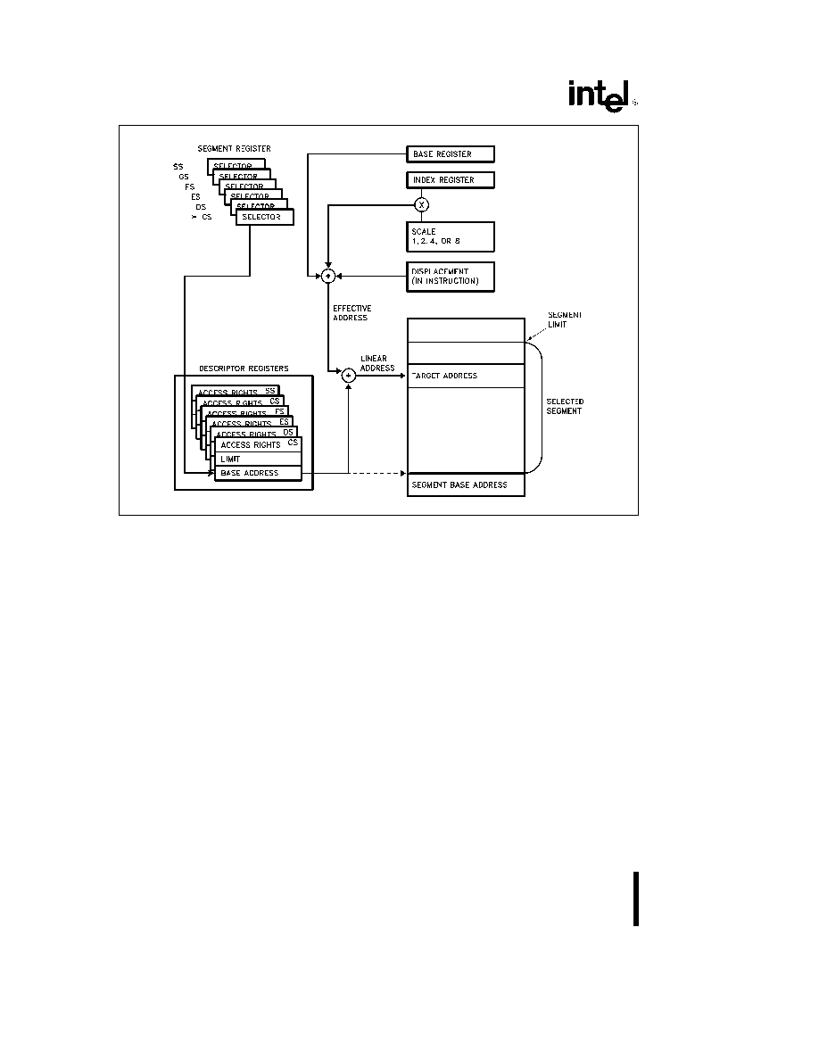
As shown in Figure 2 4 the effective address (EA) of
an operand is calculated according to the following
formula
EA
e
Base
Register
a
(Index
Register
scaling)
a
Displacement
1 Direct Mode The operand's offset is contained
as part of the instruction as an 8 16 or 32-bit
displacement
2 Register Indirect Mode A BASE register con-
tains the address of the operand
3 Based Mode A BASE register's contents are
added to a DISPLACEMENT to form the oper-
and's offset
4 Scaled Index Mode An INDEX register's con-
tents are multiplied by a SCALING factor and the
result is added to a DISPLACEMENT to form the
operand's offset
5 Based Scaled Index Mode The contents of an
INDEX register are multiplied by a SCALING fac-
tor and the result is added to the contents of a
BASE register to obtain the operand's offset
6 Based Scaled Index Mode with Displacement
The contents of an INDEX register are multiplied
by a SCALING factor and the result is added to
the contents of a BASE register and a DISPLACE-
MENT to form the operand's offset
13
Intel386
TM
SX MICROPROCESSOR
240187 � 5
Figure 2 4 Addressing Mode Calculations
DIFFERENCES BETWEEN 16 AND 32 BIT
ADDRESSES
In order to provide software compatibility with the
8086 and the 80286 the Intel386 SX Microproces-
sor can execute 16-bit instructions in Real and Pro-
tected Modes The processor determines the size of
the instructions it is executing by examining the D bit
in a Segment Descriptor If the D bit is 0 then all
operand lengths and effective addresses are as-
sumed to be 16 bits long If the D bit is 1 then the
default length for operands and addresses is 32 bits
In Real Mode the default size for operands and ad-
dresses is 16 bits
Regardless of the default precision of the operands
or addresses the Intel386 SX Microprocessor is
able to execute either 16 or 32-bit instructions This
is specified through the use of override prefixes
Two prefixes the Operand Length Prefix and the
Address Length Prefix
override the value of the D
bit on an individual instruction basis These prefixes
are automatically added by assemblers
The Operand Length and Address Length Prefixes
can be applied separately or in combination to any
instruction The Address Length Prefix does not al-
low addresses over 64K bytes to be accessed in
Real Mode
A memory address which exceeds
0FFFFH will result in a General Protection Fault An
Address Length Prefix only allows the use of the ad-
ditional Intel386 SX Microprocessor addressing
modes
When executing 32-bit code the Intel386 SX Micro-
processor uses either 8 or 32-bit displacements and
any register can be used as base or index registers
When executing 16-bit code the displacements are
either 8 or 16-bits and the base and index register
conform to the 80286 model Table 2 4 illustrates
the differences
14

Intel386
TM
SX MICROPROCESSOR
Table 2 4 BASE and INDEX Registers for 16- and 32-Bit Addresses
16-Bit Addressing
32-Bit Addressing
BASE REGISTER
BX BP
Any 32-bit GP Register
INDEX REGISTER
SI DI
Any 32-bit GP Register
Except ESP
SCALE FACTOR
None
1 2 4 8
DISPLACEMENT
0 8 16-bits
0 8 32-bits
2 5 Data Types
The Intel386 SX Microprocessor supports all of the
data types commonly used in high level languages
Bit
A single bit quantity
Bit Field
A group of up to 32 contiguous bits which
spans a maximum of four bytes
Bit String
A set of contiguous bits on the Intel386
SX Microprocessor bit strings can be up to 4 giga-
bits long
Byte
A signed 8-bit quantity
Unsigned Byte
An unsigned 8-bit quantity
Integer (Word)
A signed 16-bit quantity
Long Integer (Double Word)
A signed 32-bit quan-
tity All operations assume a 2's complement repre-
sentation
Unsigned Integer (Word)
An unsigned 16-bit
quantity
Unsigned Long Integer (Double Word)
An un-
signed 32-bit quantity
Signed Quad Word
A signed 64-bit quantity
Unsigned Quad Word
An unsigned 64-bit quantity
Pointer
A 16 or 32-bit offset-only quantity which in-
directly references another memory location
Long Pointer
A full pointer which consists of a 16-
bit segment selector and either a 16 or 32-bit offset
Char
A byte representation of an ASCII Alphanu-
meric or control character
String
A contiguous sequence of bytes words or
dwords A string may contain between 1 byte and 4
gigabytes
BCD
A byte (unpacked) representation of decimal
digits 0 � 9
Packed BCD
A byte (packed) representation of two
decimal digits 0 � 9 storing one digit in each nibble
When the Intel386 SX Microprocessor is coupled
with its numerics coprocessor the Intel387 SX then
the following common floating point types are sup-
ported
Floating Point
A signed 32 64 or 80-bit real num-
ber representation Floating point numbers are sup-
ported by the Intel387 SX numerics coprocessor
Figure 2 5 illustrates the data types supported by the
Intel386 SX Microprocessor and the Intel387 SX
2 6 I O Space
The Intel386 SX Microprocessor has two distinct
physical address spaces physical memory and I O
Generally peripherals are placed in I O space al-
though the Intel386 SX Microprocessor also sup-
ports memory-mapped peripherals The I O space
consists of 64K bytes which can be divided into 64K
8-bit ports or 32K 16-bit ports or any combination of
ports which add up to no more than 64K bytes The
64K I O address space refers to physical addresses
rather than linear addresses since I O instructions
do not go through the segmentation or paging hard-
ware The M IO
pin acts as an additional address
line thus allowing the system designer to easily de-
termine which address space the processor is ac-
cessing
The I O ports are accessed by the IN and OUT in-
structions with the port address supplied as an im-
mediate 8-bit constant in the instruction or in the DX
register All 8-bit and 16-bit port addresses are zero
extended on the upper address lines The I O in-
structions cause the M IO
pin to be driven LOW
I O port addresses 00F8H through 00FFH are re-
served for use by Intel
15

Intel386
TM
SX MICROPROCESSOR
240187 � 6
Figure 2 5 Intel386
TM
SX Microprocessor Supported Data Types
16

Intel386
TM
SX MICROPROCESSOR
2 7 Interrupts and Exceptions
Interrupts and exceptions alter the normal program
flow in order to handle external events report errors
or exceptional conditions The difference between
interrupts and exceptions is that interrupts are used
to handle asynchronous external events while ex-
ceptions handle instruction faults Although a pro-
gram can generate a software interrupt via an INT N
instruction the processor treats software interrupts
as exceptions
Hardware interrupts occur as the result of an exter-
nal event and are classified into two types maskable
or non-maskable Interrupts are serviced after the
execution of the current instruction After the inter-
rupt handler is finished servicing the interrupt exe-
cution proceeds with the instruction immediately
after
the interrupted instruction
Exceptions are classified as faults traps or aborts
depending on the way they are reported and wheth-
er or not restart of the instruction causing the excep-
tion is supported Faults are exceptions that are de-
tected and serviced before the execution of the
faulting instruction Traps are exceptions that are
reported immediately after the execution of the in-
struction which caused the problem Aborts are ex-
ceptions which do not permit the precise location of
the instruction causing the exception to be deter-
mined
Thus when an interrupt service routine has been
completed execution proceeds from the instruction
immediately following the interrupted instruction On
the other hand the return address from an excep-
tion fault routine will always point to the instruction
causing the exception and will include any leading
instruction prefixes Table 2 5 summarizes the possi-
ble interrupts for the Intel386 SX Microprocessor
and shows where the return address points to
Table 2 5 Interrupt Vector Assignments
Return Address
Interrupt
Instruction Which
Points to
Function
Number
Can Cause
Faulting
Type
Exception
Instruction
Divide Error
0
DIV IDIV
YES
FAULT
Debug Exception
1
any instruction
YES
TRAP
NMI Interrupt
2
INT 2 or NMI
NO
NMI
One Byte Interrupt
3
INT
NO
TRAP
Interrupt on Overflow
4
INTO
NO
TRAP
Array Bounds Check
5
BOUND
YES
FAULT
Invalid OP-Code
6
Any illegal instruction
YES
FAULT
Device Not Available
7
ESC WAIT
YES
FAULT
Double Fault
8
Any instruction that can
ABORT
generate an exception
Coprocessor Segment Overrun
9
ESC
NO
ABORT
Invalid TSS
10
JMP CALL IRET INT
YES
FAULT
Segment Not Present
11
Segment Register Instructions
YES
FAULT
Stack Fault
12
Stack References
YES
FAULT
General Protection Fault
13
Any Memory Reference
YES
FAULT
Page Fault
14
Any Memory Access or Code Fetch
YES
FAULT
Coprocessor Error
16
ESC WAIT
YES
FAULT
Intel Reserved
17 � 32
Two Byte Interrupt
33 � 255
INT n
NO
TRAP
Some debug exceptions may report both traps on the previous instruction and faults on the next instruction
17

Intel386
TM
SX MICROPROCESSOR
The Intel386 SX Microprocessor has the ability to
handle up to 256 different interrupts exceptions In
order to service the interrupts a table with up to 256
interrupt vectors must be defined The interrupt vec-
tors are simply pointers to the appropriate interrupt
service routine In Real Mode the vectors are 4-byte
quantities a Code Segment plus a 16-bit offset in
Protected Mode the interrupt vectors are 8 byte
quantities which are put in an Interrupt Descriptor
Table Of the 256 possible interrupts 32 are re-
served for use by Intel and the remaining 224 are
free to be used by the system designer
INTERRUPT PROCESSING
When an interrupt occurs the following actions hap-
pen First the current program address and Flags
are saved on the stack to allow resumption of the
interrupted program Next an 8-bit vector is supplied
to the Intel386 SX Microprocessor which identifies
the appropriate entry in the interrupt table The table
contains the starting address of the interrupt service
routine Then the user supplied interrupt service
routine is executed Finally when an IRET instruc-
tion is executed the old processor state is restored
and program execution resumes at the appropriate
instruction
The 8-bit interrupt vector is supplied to the Intel386
SX Microprocessor in several different ways excep-
tions supply the interrupt vector internally software
INT instructions contain or imply the vector maska-
ble hardware interrupts supply the 8-bit vector via
the interrupt acknowledge bus sequence
Non-
Maskable hardware interrupts are assigned to inter-
rupt vector 2
Maskable Interrupt
Maskable interrupts are the most common way to
respond to asynchronous external hardware events
A hardware interrupt occurs when the INTR is pulled
HIGH and the Interrupt Flag bit (IF) is enabled The
processor only responds to interrupts between in-
structions (string instructions have an `interrupt win-
dow` between memory moves which allows inter-
rupts during long string moves) When an interrupt
occurs the processor reads an 8-bit vector supplied
by the hardware which identifies the source of the
interrupt (one of 224 user defined interrupts)
Interrupts through interrupt gates automatically reset
IF disabling INTR requests Interrupts through Trap
Gates leave the state of the IF bit unchanged Inter-
rupts through a Task Gate change the IF bit accord-
ing to the image of the EFLAGs register in the task's
Task State Segment (TSS) When an IRET instruc-
tion is executed the original state of the IF bit is
restored
Non-Maskable Interrupt
Non-maskable interrupts provide a method of servic-
ing very high priority interrupts When the NMI input
is pulled HIGH it causes an interrupt with an internal-
ly supplied vector value of 2 Unlike a normal hard-
ware interrupt no interrupt acknowledgment se-
quence is performed for an NMI
While executing the NMI servicing procedure the In-
tel386 SX Microprocessor will not service any further
NMI request or INT requests until an interrupt return
(IRET) instruction is executed or the processor is
reset If NMI occurs while currently servicing an NMI
its presence will be saved for servicing after execut-
ing the first IRET instruction The IF bit is cleared at
the beginning of an NMI interrupt to inhibit further
INTR interrupts
Software Interrupts
A third type of interrupt exception for the Intel386
SX Microprocessor is the software interrupt An INT
n instruction causes the processor to execute the
interrupt service routine pointed to by the n
th
vector
in the interrupt table
A special case of the two byte software interrupt INT
n is the one byte INT 3 or breakpoint interrupt By
inserting this one byte instruction in a program the
user can set breakpoints in his program as a debug-
ging tool
A final type of software interrupt is the single step
interrupt It is discussed in Single Step Trap
18

Intel386
TM
SX MICROPROCESSOR
INTERRUPT AND EXCEPTION PRIORITIES
Interrupts are externally generated events Maska-
ble Interrupts (on the INTR input) and Non-Maskable
Interrupts (on the NMI input) are recognized at in-
struction boundaries
When NMI and maskable
INTR are both recognized at the same instruction
boundary the Intel386 SX Microprocessor invokes
the NMI service routine first If maskable interrupts
are still enabled after the NMI service routine has
been invoked then the Intel386 SX Microprocessor
will invoke the appropriate interrupt service routine
As the Intel386 SX Microprocessor executes instruc-
tions it follows a consistent cycle in checking for
exceptions as shown in Table 2 6 This cycle is re-
peated as each instruction is executed and occurs
in parallel with instruction decoding and execution
INSTRUCTION RESTART
The Intel386 SX Microprocessor fully supports re-
starting all instructions after Faults If an exception is
detected in the instruction to be executed (exception
categories 4 through 10 in Table 2 6) the Intel386
SX Microprocessor invokes the appropriate excep-
tion service routine The Intel386 SX Microprocessor
is in a state that permits restart of the instruction for
all cases but those given in Table 2 7 Note that all
such cases will be avoided by a properly designed
operating system
Table 2 6 Sequence of Exception Checking
Consider the case of the Intel386 SX Microprocessor having just completed an instruction It then performs
the following checks before reaching the point where the next instruction is completed
1 Check for Exception 1 Traps from the instruction just completed (single-step via Trap Flag or Data
Breakpoints set in the Debug Registers)
2 Check for external NMI and INTR
3 Check for Exception 1 Faults in the next instruction (Instruction Execution Breakpoint set in the Debug
Registers for the next instruction)
4 Check for Segmentation Faults that prevented fetching the entire next instruction (exceptions 11 or 13)
5 Check for Page Faults that prevented fetching the entire next instruction (exception 14)
6 Check for Faults decoding the next instruction (exception 6 if illegal opcode exception 6 if in Real Mode
or in Virtual 8086 Mode and attempting to execute an instruction for Protected Mode only or exception
13 if instruction is longer than 15 bytes or privilege violation in Protected Mode (i e not at IOPL or at
CPLe0)
7 If WAIT opcode check if TSe1 and MPe1 (exception 7 if both are 1)
8 If ESCape opcode for numeric coprocessor check if EMe1 or TSe1 (exception 7 if either are 1)
9 If WAIT opcode or ESCape opcode for numeric coprocessor check ERROR
input signal (exception 16
if ERROR
input is asserted)
10 Check in the following order for each memory reference required by the instruction
a Check for Segmentation Faults that prevent transferring the entire memory quantity (exceptions 11
12 13)
b Check for Page Faults that prevent transferring the entire memory quantity (exception 14)
NOTE
Segmentation exceptions are generated before paging exceptions
Table 2 7 Conditions Preventing Instruction Restart
1 An instruction causes a task switch to a task whose Task State Segment is partially `not present` (An
entirely `not present` TSS is restartable) Partially present TSS's can be avoided either by keeping the
TSS's of such tasks present in memory or by aligning TSS segments to reside entirely within a single 4K
page (for TSS segments of 4K bytes or less)
2 A coprocessor operand wraps around the top of a 64K-byte segment or a 4G-byte segment and spans
three pages and the page holding the middle portion of the operand is `not present` This condition can
be avoided by starting at a page boundary any segments containing coprocessor operands if the
segments are approximately 64K-200 bytes or larger (i e large enough for wraparound of the coproces-
sor operand to possibly occur)
Note that these conditions are avoided by using the operating system designs mentioned in this table
19

Intel386
TM
SX MICROPROCESSOR
Table 2 8 Register Values after Reset
Flag Word (EFLAGS)
uuuu0002H
Note 1
Machine Status Word (CR0)
uuuuuu10H
Instruction Pointer (EIP)
0000FFF0H
Code Segment (CS)
F000H
Note 2
Data Segment (DS)
0000H
Note 3
Stack Segment (SS)
0000H
Extra Segment (ES)
0000H
Note 3
Extra Segment (FS)
0000H
Extra Segment (GS)
0000H
EAX register
0000H
Note 4
EDX register
component and stepping ID
Note 5
All other registers
undefined
Note 6
NOTES
1 EFLAG Register The upper 14 bits of the EFLAGS register are undefined all defined flag bits are zero
2 The Code Segment Register (CS) will have its Base Address set to 0FFFF0000H and Limit set to 0FFFFH
3 The Data and Extra Segment Registers (DS ES) will have their Base Address set to 000000000H and Limit set to
0FFFFH
4 If self-test is selected the EAX register should contain a 0 value If a value of 0 is not found then the self-test has
detected a flaw in the part
5 EDX register always holds component and stepping identifier
6 All undefined bits are Intel Reserved and should not be used
DOUBLE FAULT
A Double Fault (exception 8) results when the proc-
essor attempts to invoke an exception service rou-
tine for the segment exceptions (10 11 12 or 13)
but in the process of doing so detects an exception
other than
a Page Fault (exception 14)
One other cause of generating a Double Fault is the
Intel386 SX Microprocessor detecting any other ex-
ception when it is attempting to invoke the Page
Fault (exception 14) service routine (for example if a
Page Fault is detected when the Intel386 SX Micro-
processor attempts to invoke the Page Fault service
routine) Of course in any functional system not
only in Intel386 SX Microprocessor-based systems
the entire page fault service routine must remain
`present` in memory
2 8 Reset and Initialization
When the processor is initialized or Reset the regis-
ters have the values shown in Table 2 8 The In-
tel386 SX Microprocessor will then start executing
instructions near the top of physical memory at lo-
cation 0FFFFF0H
When the first Intersegment
Jump or Call is executed address lines A
20
� A
23
will
drop LOW for CS-relative memory cycles and the
Intel386 SX Microprocessor will only execute in-
structions in the lower one megabyte of physical
memory This allows the system designer to use a
shadow ROM at the top of physical memory to ini-
tialize the system and take care of Resets
RESET forces the Intel386 SX Microprocessor to
terminate all execution and local bus activity No in-
struction execution or bus activity will occur as long
as Reset is active Between 350 and 450 CLK2 peri-
ods after Reset becomes inactive the Intel386 SX
Microprocessor will start executing instructions at
the top of physical memory
2 9 Testability
The Intel386 SX Microprocessor like the Intel386
Microprocessor offers testability features which in-
clude a self-test and direct access to the page trans-
lation cache
SELF-TEST
The Intel386 SX Microprocessor has the capability
to perform a self-test The self-test checks the func-
tion of all of the Control ROM and most of the non-
random logic of the part Approximately one-half of
the Intel386 SX Microprocessor can be tested during
self-test
Self-Test is initiated on the Intel386 SX Microproces-
sor when the RESET pin transitions from HIGH to
LOW and the BUSY
pin is LOW The self-test
takes about 2
20
clocks or approximately 33 millisec-
onds with a 16 MHz Intel386 SX CPU At the com-
pletion of self-test the processor performs reset and
begins normal operation The part has successfully
passed self-test if the contents of the EAX are zero
If the results of the EAX are not zero then the self-
test has detected a flaw in the part
20

Intel386
TM
SX MICROPROCESSOR
TLB TESTING
The Intel386 SX Microprocessor also provides a
mechanism for testing the Translation Lookaside
Buffer (TLB) if desired This particular mechanism
may not be continued in the same way in future
processors
There are two TLB testing operations 1) writing en-
tries into the TLB and 2) performing TLB lookups
Two Test Registers shown in Figure 2 6 are provid-
ed for the purpose of testing TR6 is the ``test com-
mand register'' and TR7 is the ``test data register''
For a more detailed explanation of testing the TLB
see the Intel386
TM
SX Microprocessor Program-
mer's Reference Manual
2 10 Debugging Support
The Intel386 SX Microprocessor provides several
features which simplify the debugging process The
three categories of on-chip debugging aids are
1 The code execution breakpoint opcode (0CCH)
2 The single-step capability provided by the TF bit
in the flag register
3 The code and data breakpoint capability provided
by the Debug Registers DR0 � 3 DR6 and DR7
BREAKPOINT INSTRUCTION
A single-byte software interrupt (Int 3) breakpoint in-
struction is available for use by software debuggers
The breakpoint opcode is 0CCh and generates an
exception 3 trap when executed
SINGLE-STEP TRAP
If the single-step flag (TF bit 8) in the EFLAG regis-
ter is found to be set at the end of an instruction a
single-step exception occurs The single-step ex-
ception is auto vectored to exception number 1
DEBUG REGISTERS
The Debug Registers are an advanced debugging
feature of the Intel386 SX Microprocessor They al-
low data access breakpoints as well as code execu-
tion breakpoints Since the breakpoints are indicated
by on-chip registers an instruction execution break-
point can be placed in ROM code or in code shared
by several tasks neither of which can be supported
by the INT 3 breakpoint opcode
The Intel386 SX Microprocessor contains six Debug
Registers consisting of four breakpoint address reg-
isters and two breakpoint control registers Initially
after reset breakpoints are in the disabled state
therefore no breakpoints will occur unless the de-
bug registers are programmed Breakpoints set up in
the Debug Registers are auto-vectored to exception
1 Figure 2 7 shows the breakpoint status and con-
trol registers
240187 � 7
Figure 2 6 Test Registers
21

Intel386
TM
SX MICROPROCESSOR
240187 � 8
Figure 2 7 Debug Registers
3 0 REAL MODE ARCHITECTURE
When the processor is reset or powered up it is ini-
tialized in Real Mode Real Mode has the same base
architecture as the 8086 but allows access to the
32-bit register set of the Intel386 SX Microproces-
sor The addressing mechanism memory size and
interrupt handling are all identical to the Real Mode
on the 80286
The default operand size in Real Mode is 16 bits as
in the 8086 In order to use the 32-bit registers and
addressing modes override prefixes must be used
In addition the segment size on the Intel386 SX Mi-
croprocessor in Real Mode is 64K bytes so 32-bit
addresses must have a value less then 0000FFFFH
The primary purpose of Real Mode is to set up the
processor for Protected Mode operation
3 1 Memory Addressing
In Real Mode the linear addresses are the same as
physical addresses (paging is not allowed) Physical
addresses are formed in Real Mode by adding the
contents of the appropriate segment register which
is shifted left by four bits to an effective address
This addition results in a 20-bit physical address or a
1 megabyte address space Since segment registers
are shifted left by 4 bits Real Mode segments al-
ways start on 16-byte boundaries
All segments in Real Mode are exactly 64K bytes
long and may be read written or executed The
Intel386 SX Microprocessor will generate an excep-
tion 13 if a data operand or instruction fetch occurs
past the end of a segment
22
Intel386
TM
SX MICROPROCESSOR
Table 3 1 Exceptions in Real Mode
Function
Interrupt
Related
Return
Number
Instructions
Address Location
Interrupt table limit
8
INT vector is not
Before
too small
within table limit
Instruction
CS DS ES FS GS
13
Word memory reference
Before
Segment overrun exception
with offset e 0FFFFH
Instruction
an attempt to execute
past the end of CS segment
SS Segment overrun
12
Stack Reference
Before
exception
beyond offset e 0FFFFH
Instruction
3 2 Reserved Locations
There are two fixed areas in memory which are re-
served in Real address mode the system initializa-
tion area and the interrupt table area Locations
00000H through 003FFH are reserved for interrupt
vectors Each one of the 256 possible interrupts has
a 4-byte jump vector reserved for it
Locations
0FFFFF0H through 0FFFFFFH are reserved for sys-
tem initialization
3 3 Interrupts
Many of the exceptions discussed in section 2 7 are
not applicable to Real Mode operation in particular
exceptions 10 11 and 14 do not occur in Real
Mode
Other exceptions have slightly different
meanings in Real Mode Table 3 1 identifies these
exceptions
3 4 Shutdown and Halt
The HLT instruction stops program execution and
prevents the processor from using the local bus until
restarted Either NMI FLT
INTR with interrupts
enabled (IFe1) or RESET will force the Intel386 SX
Microprocessor out of halt If interrupted the saved
CS IP will point to the next instruction after the HLT
Shutdown will occur when a severe error is detected
that prevents further processing In Real Mode
shutdown can occur under two conditions
1 An interrupt or an exception occurs (Exceptions 8
or 13) and the interrupt vector is larger than the
Interrupt Descriptor Table
2 A CALL INT or PUSH instruction attempts to
wrap around the stack segment when SP is not
even
An NMI input can bring the processor out of shut-
down if the Interrupt Descriptor Table limit is large
enough to contain the NMI interrupt vector (at least
000FH) and the stack has enough room to contain
the vector and flag information (i e SP is greater that
0005H) Otherwise shutdown can only be exited by
a processor reset
3 5 LOCK Operation
The LOCK prefix on the Intel386 SX Microprocessor
even in Real Mode is more restrictive than on the
80286 This is due to the addition of paging on the
Intel386 SX Microprocessor in Protected Mode and
Virtual 8086 Mode The LOCK prefix is not support-
ed during repeat string instructions
The only instruction forms where the LOCK prefix is
legal on the Intel386 SX Microprocessor are shown
in Table 3 2
Table 3 2 Legal Instructions for the LOCK Prefix
Opcode
Operands
(Dest Source)
BIT Test and
SET RESET
Mem Reg Immediate
COMPLEMENT
XCHG
Reg Mem
XCHG
Mem Reg
ADD OR ADC SBB
AND SUB XOR
Mem Reg Immediate
NOT NEG INC DEC
Mem
An exception 6 will be generated if a LOCK prefix is
placed before any instruction form or opcode not
listed above The LOCK prefix allows indivisible
read modify write operations on memory operands
using the instructions above
The LOCK prefix is not IOPL-sensitive on the
Intel386 SX Microprocessor The LOCK prefix can
be used at any privilege level but only on the in-
struction forms listed in Table 3 2
23

Intel386
TM
SX MICROPROCESSOR
4 0 PROTECTED MODE
ARCHITECTURE
The complete capabilities of the Intel386 SX Micro-
processor are unlocked when the processor oper-
ates in Protected Virtual Address Mode (Protected
Mode) Protected Mode vastly increases the linear
address space to four gigabytes (2
32
bytes) and al-
lows the running of virtual memory programs of al-
most unlimited size (64 terabytes (2
46
bytes)) In ad-
dition Protected Mode allows the Intel386 SX Micro-
processor to run all of the existing Intel386 DX CPU
(using only 16 megabytes of physical memory)
80286 and 8086 CPU's software while providing a
sophisticated memory management and a hard-
ware-assisted
protection
mechanism
Protected
Mode allows the use of additional instructions spe-
cially optimized for supporting multitasking operating
systems The base architecture of the Intel386 SX
Microprocessor remains the same the registers in-
structions and addressing modes described in the
previous sections are retained The main difference
between Protected Mode and Real Mode from a
programmer's viewpoint is the increased address
space and a different addressing mechanism
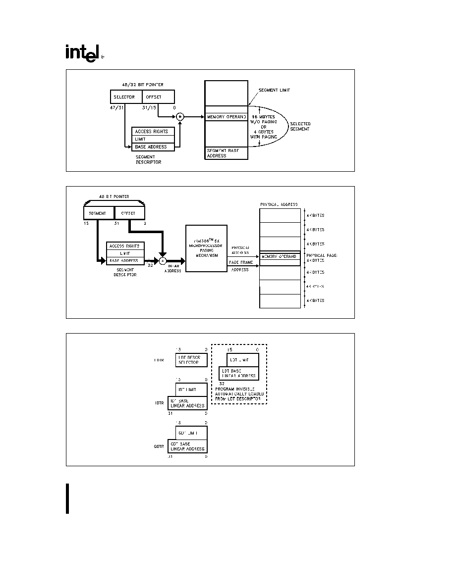
4 1 Addressing Mechanism
Like Real Mode Protected Mode uses two compo-
nents to form the logical address a 16-bit selector is
used to determine the linear base address of a seg-
ment the base address is added to a 32-bit effective
address to form a 32-bit linear address The linear
address is then either used as a 24-bit physical ad-
dress or if paging is enabled the paging mechanism
maps the 32-bit linear address into a 24-bit physical
address
The difference between the two modes lies in calcu-
lating the base address In Protected Mode the se-
lector is used to specify an index into an operating
system defined table (see Figure 4 1) The table
contains the 32-bit base address of a given seg-
ment The physical address is formed by adding the
base address obtained from the table to the offset
Paging provides an additional memory management
mechanism which operates only in Protected Mode
Paging provides a means of managing the very large
segments of the Intel386 SX Microprocessor as
paging operates beneath segmentation The page
mechanism translates the protected linear address
which comes from the segmentation unit into a
physical address Figure 4 2 shows the complete In-
tel386 SX Microprocessor addressing mechanism
with paging enabled
4 2 Segmentation
Segmentation is one method of memory manage-
ment Segmentation provides the basis for protec-
tion Segments are used to encapsulate regions of
memory which have common attributes For exam-
ple all of the code of a given program could be con-
tained in a segment or an operating system table
may reside in a segment All information about each
segment is stored in an 8 byte data structure called
a descriptor All of the descriptors in a system are
contained in descriptor tables which are recognized
by hardware
TERMINOLOGY
The following terms are used throughout the discus-
sion of descriptors privilege levels and protection
PL
Privilege Level
One of the four hierarchical
privilege levels Level 0 is the most privileged
level and level 3 is the least privileged
RPL Requestor Privilege Level
The privilege level
of the original supplier of the selector RPL is
determined by the least two significant bits of
a selector
DPL Descriptor Privilege Level
This is the least
privileged level at which a task may access
that descriptor (and the segment associated
with that descriptor) Descriptor Privilege Lev-
el is determined by bits 6 5 in the Access
Right Byte of a descriptor
CPL Current Privilege Level
The privilege level at
which a task is currently executing which
equals the privilege level of the code segment
being executed CPL can also be determined
by examining the lowest 2 bits of the CS regis-
ter except for conforming code segments
EPL Effective Privilege Level
The effective privi-
lege level is the least privileged of the RPL
and the DPL EPL is the numerical maximum
of RPL and DPL
Task One instance of the execution of a program
Tasks are also referred to as processes
DESCRIPTOR TABLES
The descriptor tables define all of the segments
which are used in a Intel386 SX Microprocessor sys-
tem There are three types of tables which hold de-
scriptors the Global Descriptor Table Local De-
scriptor Table and the Interrupt Descriptor Table All
of the tables are variable length memory arrays and
can vary in size from 8 bytes to 64K bytes Each
table can hold up to 8192 8-byte descriptors The
upper 13 bits of a selector are used as an index into
the descriptor table The tables have registers asso-
ciated with them which hold the 32-bit linear base
address and the 16-bit limit of each table
24
Intel386
TM
SX MICROPROCESSOR
240187 � 9
Figure 4 1 Protected Mode Addressing
240187 � 10
Figure 4 2 Paging and Segmentation
240187 � 11
Figure 4 3 Descriptor Table Registers
25
Intel386
TM
SX MICROPROCESSOR
Each of the tables has a register associated with it
GDTR LDTR and IDTR see Figure 2 1 The LGDT
LLDT and LIDT instructions load the base and limit
of the Global Local and Interrupt Descriptor Tables
into the appropriate register The SGDT SLDT and
SIDT store the base and limit values These are priv-
ileged instructions
Global Descriptor Table
The Global Descriptor Table (GDT) contains de-
scriptors which are available to all of the tasks in a
system The GDT can contain any type of segment
descriptor except for interrupt and trap descriptors
Every Intel386 SX CPU system contains a GDT
The first slot of the Global Descriptor Table corre-
sponds to the null selector and is not used The null
selector defines a null pointer value
Local Descriptor Table
LDTs contain descriptors which are associated with
a given task Generally operating systems are de-
signed so that each task has a separate LDT The
LDT may contain only code data stack task gate
and call gate descriptors LDTs provide a mecha-
nism for isolating a given task's code and data seg-
ments from the rest of the operating system while
the GDT contains descriptors for segments which
are common to all tasks A segment cannot be ac-
cessed by a task if its segment descriptor does not
exist in either the current LDT or the GDT This pro-
vides both isolation and protection for a task's seg-
ments while still allowing global data to be shared
among tasks
Unlike the 6-byte GDT or IDT registers which contain
a base address and limit the visible portion of the
LDT register contains only a 16-bit selector This se-
lector refers to a Local Descriptor Table descriptor in
the GDT (see figure 2 1)
Interrupt Descriptor Table
The third table needed for Intel386 SX Microproces-
sor systems is the Interrupt Descriptor Table The
IDT contains the descriptors which point to the loca-
tion of the up to 256 interrupt service routines The
IDT may contain only task gates interrupt gates and
trap gates The IDT should be at least 256 bytes in
size in order to hold the descriptors for the 32 Intel
Reserved Interrupts Every interrupt used by a sys-
tem must have an entry in the IDT The IDT entries
are referenced by INT instructions external interrupt
vectors and exceptions
DESCRIPTORS
The object to which the segment selector points to
is called a descriptor Descriptors are eight byte
quantities which contain attributes about a given re-
gion of linear address space These attributes in-
clude the 32-bit base linear address of the segment
the 20-bit length and granularity of the segment the
protection level read write or execute privileges
the default size of the operands (16-bit or 32-bit)
and the type of segment All of the attribute informa-
tion about a segment is contained in 12 bits in the
segment descriptor Figure 4 4 shows the general
format of a descriptor All segments on the Intel386
SX Microprocessor have three attribute fields in
common the P bit the DPL bit and the S bit The P
31
0
BYTE
SEGMENT BASE 15
0
SEGMENT LIMIT 15
0
ADDRESS
0
BASE 31
24
G
D
0
AVL
LIMIT
P
DPL
S
TYPE
A
BASE
a
4
19
16
23
16
BASE
Base Address of the segment
LIMIT
The length of the segment
P
Present Bit
1ePresent
0eNot Present
DPL
Descriptor Privilege Level 0 � 3
S
Segment Descriptor
0eSystem Descriptor
1eCode or Data Segment Descriptor
TYPE
Type of Segment
A
Accessed Bit
G
Granularity Bit
1eSegment length is page granular
0eSegment length is byte granular
D
Default Operation Size (recognized in code segment descriptors only)
1e32-bit segment
0e16-bit segment
0
Bit must be zero (0) for compatibility with future processors
AVL
Available field for user or OS
Figure 4 4 Segment Descriptors
26

Intel386
TM
SX MICROPROCESSOR
(Present) Bit is 1 if the segment is loaded in physical
memory If Pe0 then any attempt to access this
segment causes a not present exception (exception
11) The Descriptor Privilege Level DPL is a two bit
field which specifies the protection level 0 � 3 asso-
ciated with a segment
The Intel386 SX Microprocessor has two main cate-
gories of segments system segments and non-sys-
tem segments (for code and data) The segment bit
S determines if a given segment is a system seg-
ment or a code or data segment If the S bit is 1 then
the segment is either a code or data segment if it is
0 then the segment is a system segment
Code and Data Descriptors (Se1)
Figure 4 5 shows the general format of a code and
data descriptor and Table 4 1 illustrates how the bits
in the Access Right Byte are interpreted
31
0
SEGMENT BASE 15
0
SEGMENT LIMIT 15
0
0
LIMIT
ACCESS
BASE
BASE 31
24
G
D
0
AVL
19
16
RIGHTS
23
16
a
4
BYTE
D B
1eDefault Instructions Attributes are 32-Bits
0eDefault Instruction Attributes are 16-Bits
AVL
Available field for user or OS
G
Granularity Bit
1eSegment length is page granular
0eSegment length is byte granular
0
Bit must be zero (0) for compatibility with future processors
Figure 4 5 Code and Data Descriptors
Table 4 1 Access Rights Byte Definition for Code and Data Descriptors
Bit
Name
Function
Position
7
Present (P)
P e 1
Segment is mapped into physical memory
P e 0
No mapping to physical memory exists base and limt are
not used
6 � 5
Descriptor Privilege
Segment privilege attribute used in privilege tests
Level (DPL)
4
Segment Descrip-
S e 1
Code or Data (includes stacks) segment descriptor
tor (S)
S e 0
System Segment Descriptor or Gate Descriptor
3
Executable (E)
E e 0
Descriptor type is data segment
If
2
Expansion Direc-
ED e 0 Expand up segment offsets must be
s
limit
Data
tion (ED)
ED e 1 Expand down segment offsets must be
l
limit
Segment
1
Writeable (W)
W e 0 Data segment may not be written into
(S e 1
W e 1 Data segment may be written into
*
E e 0)
3
Executable (E)
E e 1
Descriptor type is code segment
If
2
Conforming (C)
C e 1
Code segment may only be executed
Code
when CPL
t
DPL and CPL
Segment
remains unchanged
(S e 1
1
Readable (R)
R e 0 Code segment may not be read
E e 1)
R e 1 Code segment may be read
*
0
Accessed (A)
A e 0
Segment has not been accessed
A e 1
Segment selector has been loaded into segment register
or used by selector test instructions
27

Intel386
TM
SX MICROPROCESSOR
31
16
0
SEGMENT BASE 15
0
SEGMENT LIMIT 15
0
0
BASE 31
24
G
0
0
0
LIMIT
P
DPL
0
TYPE
BASE
a
4
19
16
23
16
Type
Defines
0
Invalid
1
Available 80286 TSS
2
LDT
3
Busy 80286 TSS
4
80286 Call Gate
5
Task Gate (for 80286 or Intel386
TM
SX
Microprocessor Task)
6
80286 Interrupt Gate
7
80286 Trap Gate
Type
Defines
8
Invalid
9
Available Intel386
TM
SX Microprocessor TSS
A
Undefined (Intel Reserved)
B
Busy Intel386
TM
SX Microprocessor TSS
C
Intel386
TM
SX Microprocessor Call Gate
D
Undefined (Intel Reserved)
E
Intel386
TM
SX Microprocessor Interrupt Gate
F
Intel386
TM
SX Microprocessor Trap Gate
Figure 4 6 System Descriptors
Code and data segments have several descriptor
fields in common The accessed bit A is set when-
ever the processor accesses a descriptor The gran-
ularity bit G specifies if a segment length is byte-
granular or page-granular
System Descriptor Formats (Se0)
System segments describe information about oper-
ating system tables tasks and gates Figure 4 6
shows the general format of system segment de-
scriptors and the various types of system segments
Intel386 SX system descriptors (which are the same
as Intel386 DX CPU system descriptors) contain a
32-bit base linear address and a 20-bit segment lim-
it 80286 system descriptors have a 24-bit base ad-
dress and a 16-bit segment limit 80286 system de-
scriptors are identified by the upper 16 bits being all
zero
Differences Between Intel386
TM
SX
Microprocessor and 80286 Descriptors
In order to provide operating system compatibility
with the 80286 the Intel386 SX CPU supports all of
the 80286 segment descriptors The 80286 system
segment descriptors contain a 24-bit base address
and 16-bit limit while the Intel386 SX CPU system
segment descriptors have a 32-bit base address a
20-bit limit field and a granularity bit The word count
field specifies the number of 16-bit quantities to copy
for 80286 call gates and 32-bit quantities for
Intel386 SX CPU call gates
Selector Fields
A selector in Protected Mode has three fields Local
or Global Descriptor Table indicator (TI) Descriptor
Entry Index (Index) and Requestor (the selector's)
Privilege Level (RPL) as shown in Figure 4 7 The TI
bit selects either the Global Descriptor Table or the
Local Descriptor Table The Index selects one of 8k
descriptors in the appropriate descriptor table The
RPL bits allow high speed testing of the selector's
privilege attributes
Segment Descriptor Cache
In addition to the selector value every segment reg-
ister has a segment descriptor cache register asso-
ciated with it Whenever a segment register's con-
tents are changed the 8-byte descriptor associated
with that selector is automatically loaded (cached)
on the chip Once loaded all references to that seg-
ment use the cached descriptor information instead
of reaccessing the descriptor The contents of the
descriptor cache are not visible to the programmer
Since descriptor caches only change when a seg-
ment register is changed programs which modify
the descriptor tables must reload the appropriate
segment registers after changing a descriptor's val-
ue
28
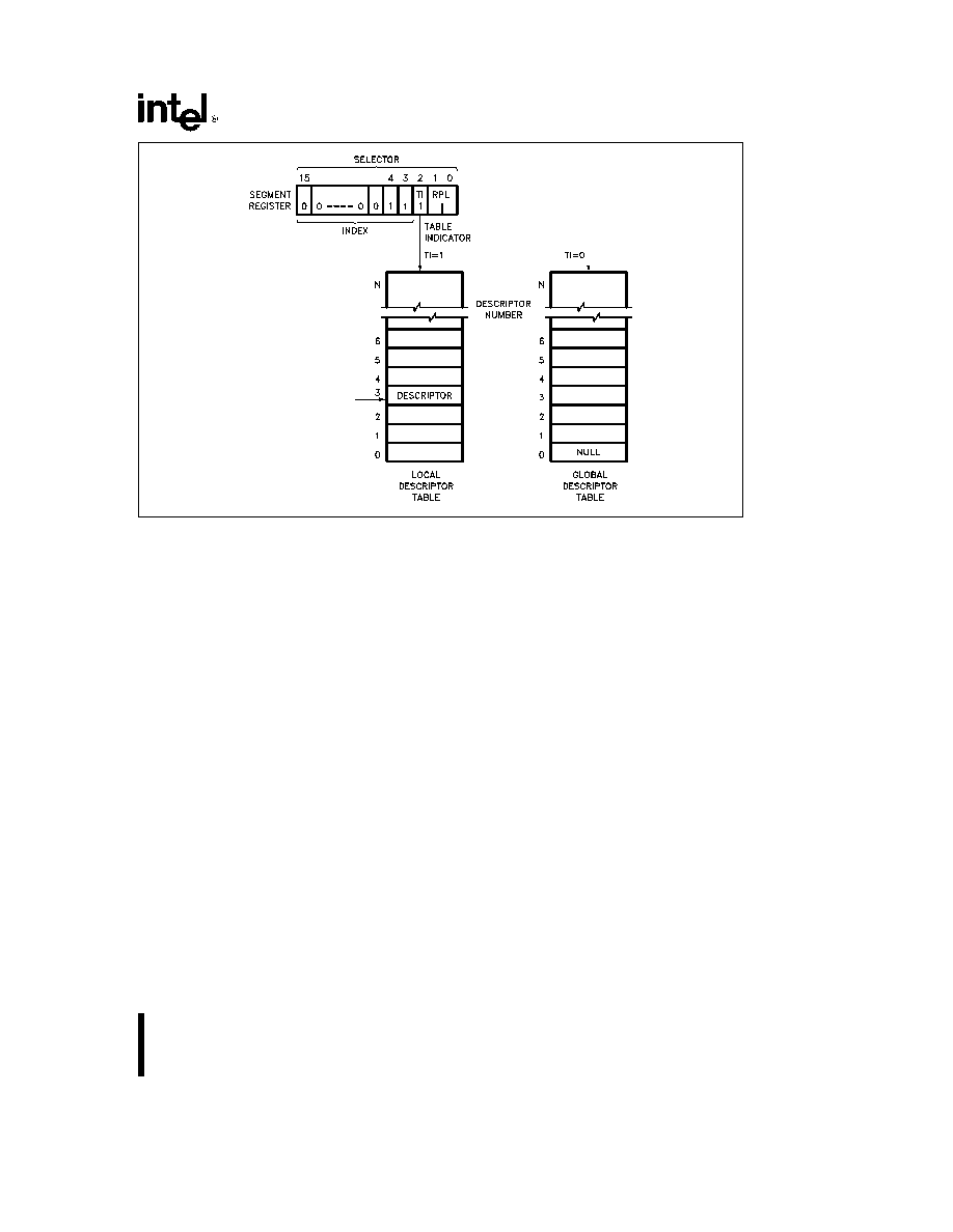
Intel386
TM
SX MICROPROCESSOR
240187 � 12
Figure 4 7 Example Descriptor Selection
4 3 Protection
The Intel386 SX Microprocessor has four levels of
protection which are optimized to support a multi-
tasking operating system and to isolate and protect
user programs from each other and the operating
system The privilege levels control the use of privi-
leged instructions I O instructions and access to
segments and segment descriptors The Intel386 SX
Microprocessor also offers an additional type of pro-
tection on a page basis when paging is enabled
The four-level hierarchical privilege system is an ex-
tension of the user supervisor privilege mode com-
monly used by minicomputers The user supervisor
mode is fully supported by the Intel386 SX Micro-
processor paging mechanism The privilege levels
(PL) are numbered 0 through 3 Level 0 is the most
privileged level
RULES OF PRIVILEGE
The Intel386 SX Microprocessor controls access to
both data and procedures between levels of a task
according to the following rules
Data stored in a segment with privilege level p
can be accessed only by code executing at a
privilege level at least as privileged as p
A code segment procedure with privilege level p
can only be called by a task executing at the
same or a lesser privilege level than p
PRIVILEGE LEVELS
At any point in time a task on the Intel386 SX Micro-
processor always executes at one of the four privi-
lege levels The Current Privilege Level (CPL) speci-
fies what the task's privilege level is A task's CPL
may only be changed by control transfers through
gate descriptors to a code segment with a different
privilege level Thus an application program running
at PLe3 may call an operating system routine at
PLe1 (via a gate) which would cause the task's CPL
to be set to 1 until the operating system routine was
finished
Selector Privilege (RPL)
The privilege level of a selector is specified by the
RPL field The selector's RPL is only used to estab-
lish a less trusted privilege level than the current
privilege level of the task for the use of a segment
This level is called the task's effective privilege level
(EPL) The EPL is defined as being the least privi-
leged (numerically larger) level of a task's CPL and a
selector's RPL The RPL is most commonly used to
verify that pointers passed to an operating system
procedure do not access data that is of higher privi-
lege than the procedure that originated the pointer
Since the originator of a selector can specify any
RPL value the Adjust RPL (ARPL) instruction is pro-
vided to force the RPL bits to the originator's CPL
29
Intel386
TM
SX MICROPROCESSOR
Table 4 2 Descriptor Types Used for Control Transfer
Control Transfer Types
Operation Types
Descriptor
Descriptor
Referenced
Table
Intersegment within the same privilege level
JMP CALL RET IRET
Code Segment
GDT LDT
Intersegment to the same or higher privilege level
CALL
Call Gate
GDT LDT
Interrupt within task may change CPL
Interrupt instruction
Trap or
IDT
Exception External
Interrupt
Interrupt
Gate
Intersegment to a lower privilege level
RET IRET
Code Segment
GDT LDT
(changes task CPL)
CALL JMP
Task State
GDT
Segment
Task Switch
CALL JMP
Task Gate
GDT LDT
IRET
Task Gate
IDT
Interrupt instruction
Exception External
Interrupt
NT (Nested Task bit of flag register)
e
0
NT (Nested Task bit of flag register)
e
1
I O Privilege
The I O privilege level (IOPL) lets the operating sys-
tem code executing at CPLe0 define the least privi-
leged level at which I O instructions can be used An
exception 13 (General Protection Violation) is gener-
ated if an I O instruction is attempted when the CPL
of the task is less privileged then the IOPL The
IOPL is stored in bits 13 and 14 of the EFLAGS reg-
ister The following instructions cause an exception
13 if the CPL is greater than IOPL IN INS OUT
OUTS STI CLI LOCK prefix
Descriptor Access
There are basically two types of segment accesses
those involving code segments such as control
transfers and those involving data accesses Deter-
mining the ability of a task to access a segment in-
volves the type of segment to be accessed the in-
struction used the type of descriptor used and CPL
RPL and DPL as described above
Any time an instruction loads a data segment regis-
ter (DS ES FS GS) the Intel386 SX Microprocessor
makes protection validation checks Selectors load-
ed in the DS ES FS GS registers must refer only to
data segment or readable code segments
Finally the privilege validation checks are performed
The CPL is compared to the EPL and if the EPL is
more privileged than the CPL an exception 13 (gen-
eral protection fault) is generated
The rules regarding the stack segment are slightly
different than those involving data segments In-
structions that load selectors into SS must refer to
data segment descriptors for writeable data seg-
ments The DPL and RPL must equal the CPL of all
other descriptor types or a privilege level violation
will cause an exception 13 A stack not present fault
causes an exception 12
PRIVILEGE LEVEL TRANSFERS
Inter-segment control transfers occur when a selec-
tor is loaded in the CS register For a typical system
most of these transfers are simply the result of a call
or a jump to another routine There are five types of
control transfers which are summarized in Table 4 2
Many of these transfers result in a privilege level
transfer Changing privilege levels is done only by
control transfers using gates task switches and in-
terrupt or trap gates
Control transfers can only occur if the operation
which loaded the selector references the correct de-
scriptor type Any violation of these descriptor usage
rules will cause an exception 13
30

Intel386
TM
SX MICROPROCESSOR
240187 � 13
Type
e
9 Available Intel386
TM
SX Microprocessor TSS
Type
e
B Busy Intel386 SX Microprocessor TSS
Figure 4 8 Intel386
TM
SX Microprocessor TSS and TSS Registers
31

Intel386
TM
SX MICROPROCESSOR
240187 � 14
I O Ports Accessible 2
x
9 12 13 15 20
x
24 27 33 34 40 41 48 50 52 53 58
x
60 62 63 96
x
127
Figure 4 9 Sample I O Permission Bit Map
CALL GATES
Gates provide protected indirect CALLs One of the
major uses of gates is to provide a secure method of
privilege transfers within a task Since the operating
system defines all of the gates in a system it can
ensure that all gates only allow entry into a few trust-
ed procedures
TASK SWITCHING
A very important attribute of any multi-tasking multi-
user operating system is its ability to rapidly switch
between tasks or processes The Intel386 SX Micro-
processor directly supports this operation by provid-
ing a task switch instruction in hardware The task
switch operation saves the entire state of the ma-
chine (all of the registers address space and a link
to the previous task) loads a new execution state
performs protection checks and commences execu-
tion in the new task Like transfer of control by
gates the task switch operation is invoked by exe-
cuting an inter-segment JMP or CALL instruction
which refers to a Task State Segment (TSS) or a
task gate descriptor in the GDT or LDT An INT n
instruction exception trap or external interrupt may
also invoke the task switch operation if there is a
task gate descriptor in the associated IDT descriptor
slot
The TSS descriptor points to a segment (see Figure
4 8) containing the entire execution state A task
gate descriptor contains a TSS selector
The
Intel386 SX Microprocessor supports both the
80286 and Intel386 SX CPU TSSs The limit of a
Intel386 SX Microprocessor TSS must be greater
than 64H (2BH for an 80286 TSS) and can be as
large as 16 megabytes In the additional TSS space
the operating system is free to store additional infor-
mation such as the reason the task is inactive time
the task has spent running or open files belonging
to the task
Each task must have a TSS associated with it The
current TSS is identified by a special register in the
Intel386 SX Microprocessor called the Task State
Segment Register (TR) This register contains a se-
lector referring to the task state segment descriptor
that defines the current TSS A hidden base and limit
register associated with TSS descriptor are loaded
whenever TR is loaded with a new selector Return-
ing from a task is accomplished by the IRET instruc-
tion When IRET is executed control is returned to
the task which was interrupted The currently exe-
cuting task's state is saved in the TSS and the old
task state is restored from its TSS
Several bits in the flag register and machine status
word (CR0) give information about the state of a
task which is useful to the operating system The
Nested Task bit NT controls the function of the
IRET instruction If NTe0 the IRET instruction per-
forms the regular return If NTe1 IRET performs a
task switch operation back to the previous task The
NT bit is set or reset in the following fashion
When a CALL or INT instruction initiates a task
switch the new TSS will be marked busy and
the back link field of the new TSS set to the old
TSS selector The NT bit of the new task is set
by CALL or INT initiated task switches An in-
terrupt that does not cause a task switch will
clear NT (The NT bit will be restored after exe-
cution of the interrupt handler) NT may also be
set or cleared by POPF or IRET instructions
The Intel386 SX Microprocessor task state segment
is marked busy by changing the descriptor type field
from TYPE 9 to TYPE 0BH An 80286 TSS is
marked busy by changing the descriptor type field
from TYPE 1 to TYPE 3 Use of a selector that refer-
ences a busy task state segment causes an excep-
tion 13
The VM (Virtual Mode) bit is used to indicate if a task
is a Virtual 8086 task If VMe1 then the tasks will
use the Real Mode addressing mechanism The vir-
tual 8086 environment is only entered and exited by
a task switch
The coprocessor's state is not automatically saved
when a task switch occurs The Task Switched Bit
TS in the CR0 register helps deal with the coproces-
sor's state in a multi-tasking environment Whenever
the Intel386 SX Microprocessor switches task it
sets the TS bit The Intel386 SX Microprocessor de-
tects the first use of a processor extension instruc-
tion after a task switch and causes the processor
extension not available exception 7 The exception
handler for exception 7 may then decide whether to
save the state of the coprocessor
The T bit in the Intel386 SX Microprocessor TSS
indicates that the processor should generate a de-
bug exception when switching to a task If Te1 then
upon entry to a new task a debug exception 1 will be
generated
32
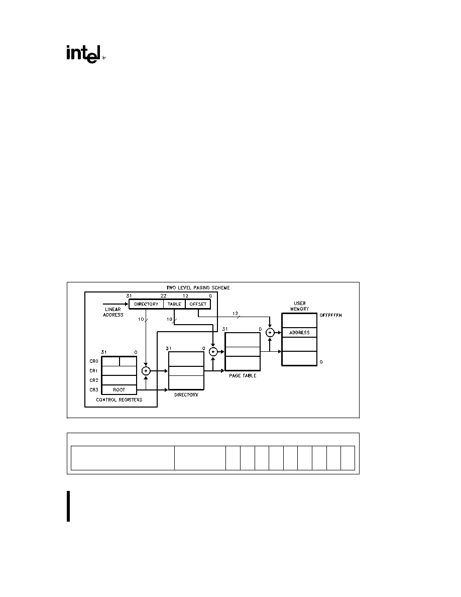
Intel386
TM
SX MICROPROCESSOR
INITIALIZATION AND TRANSITION TO
PROTECTED MODE
Since the Intel386 SX Microprocessor begins exe-
cuting in Real Mode immediately after RESET it is
necessary to initialize the system tables and regis-
ters with the appropriate values The GDT and IDT
registers must refer to a valid GDT and IDT The IDT
should be at least 256 bytes long and the GDT must
contain descriptors for the initial code and data seg-
ments
Protected Mode is enabled by loading CR0 with PE
bit set This can be accomplished by using the MOV
CR0
R M
instruction
After enabling Protected
Mode the next instruction should execute an inter-
segment JMP to load the CS register and flush the
instruction decode queue The final step is to load all
of the data segment registers with the initial selector
values
An alternate approach to entering Protected Mode is
to use the built in task-switch to load all of the regis-
ters In this case the GDT would contain two TSS
descriptors in addition to the code and data descrip-
tors needed for the first task The first JMP instruc-
tion in Protected Mode would jump to the TSS caus-
ing a task switch and loading all of the registers with
the values stored in the TSS The Task State Seg-
ment Register should be initialized to point to a valid
TSS descriptor
4 4 Paging
Paging is another type of memory management use-
ful for virtual memory multi-tasking operating sys-
tems Unlike segmentation which modularizes pro-
grams and data into variable length segments pag-
ing divides programs into multiple uniform size
pages Pages bear no direct relation to the logical
structure of a program While segment selectors can
be considered the logical `name` of a program mod-
ule or data structure a page most likely corresponds
to only a portion of a module or data structure
PAGE ORGANIZATION
The Intel386 SX Microprocessor uses two levels of
tables to translate the linear address (from the seg-
mentation unit) into a physical address There are
three components to the paging mechanism of the
Intel386 SX Microprocessor the page directory the
page tables and the page itself (page frame) All
memory-resident elements of the Intel386 SX Micro-
processor paging mechanism are the same size
namely 4K bytes A uniform size for all of the ele-
ments simplifies memory allocation and reallocation
schemes since there is no problem with memory
fragmentation Figure 4 10 shows how the paging
mechanism works
240187 � 15
Figure 4 10 Paging Mechanism
31
12
11
10
9
8
7
6
5
4
3
2
1
0
System
U
R
PAGE TABLE ADDRESS 31 12
Software
0
0
D
A
0
0
P
Defineable
S
W
Figure 4 11 Page Directory Entry (Points to Page Table)
33

Intel386
TM
SX MICROPROCESSOR
31
12
11
10
9
8
7
6
5
4
3
2
1
0
System
U
R
PAGE FRAME ADDRESS 31 12
Software
0
0
D
A
0
0
P
Defineable
S
W
Figure 4 12 Page Table Entry (Points to Page)
Page Fault Register
CR2 is the Page Fault Linear Address register It
holds the 32-bit linear address which caused the last
Page Fault detected
Page Descriptor Base Register
CR3 is the Page Directory Physical Base Address
Register It contains the physical starting address of
the Page Directory (this value is truncated to a 24-bit
value associated with the Intel386 SX CPU's 16
megabyte physical memory limitation) The lower 12
bits of CR3 are always zero to ensure that the Page
Directory is always page aligned Loading it with a
MOV CR3 reg
instruction causes the page table en-
try cache to be flushed as will a task switch through
a TSS which changes the value of CR0
Page Directory
The Page Directory is 4k bytes long and allows up to
1024 page directory entries Each page directory en-
try contains information about the page table and
the address of the next level of tables the Page
Tables The contents of a Page Directory Entry are
shown in figure 4 11 The upper 10 bits of the linear
address (A
31
� A
22
) are used as an index to select
the correct Page Directory Entry
The page table address contains the upper 20 bits
of a 32-bit physical address that is used as the base
address for the next set of tables the page tables
The lower 12 bits of the page table address are zero
so that the page table addresses appear on 4 kbyte
boundaries For a Intel386 DX CPU system the up-
per 20 bits will select one of 2
20
page tables but for
a Intel386 SX Microprocessor system the upper 20
bits only select one of 2
12
page tables Again this is
because the Intel386 SX Microprocessor is limited to
a 24-bit physical address and the upper 8 bits (A
24
�
A
31
) are truncated when the address is output on its
24 address pins
Page Tables
Each Page Table is 4K bytes long and allows up to
1024 Page table Entries Each page table entry con-
tains information about the Page Frame and its ad-
dress The contents of a Page Table Entry are
shown in figure 4 12 The middle 10 bits of the linear
address (A
21
� A
12
) are used as an index to select
the correct Page Table Entry
The Page Frame Address contains the upper 20 bits
of a 32-bit physical address that is used as the base
address for the Page Frame The lower 12 bits of the
Page Frame Address are zero so that the Page
Frame addresses appear on 4 kbyte boundaries For
an Intel386 DX CPU system the upper 20 bits will
select one of 2
20
Page Frames
but for an
Intel386 SX Microprocessor system the upper 20
bits only select one of 2
12
Page Frames Again this
is because the Intel386 SX Microprocessor is limited
to a 24-bit physical address space and the upper 8
bits (A
24
� A
31
) are truncated when the address is
output on its 24 address pins
Page Directory Table Entries
The lower 12 bits of the Page Table Entries and
Page Directory Entries contain statistical information
about pages and page tables respectively The P
(Present) bit indicates if a Page Directory or Page
Table entry can be used in address translation If
Pe1 the entry can be used for address translation
If Pe0 the entry cannot be used for translation All
of the other bits are available for use by the soft-
ware For example the remaining 31 bits could be
used to indicate where on disk the page is stored
The A (Accessed) bit is set by the Intel386 SX CPU
for both types of entries before a read or write ac-
cess occurs to an address covered by the entry The
D (Dirty) bit is set to 1 before a write to an address
covered by that page table entry occurs The D bit is
undefined for Page Directory Entries When the P A
and D bits are updated by the Intel386 SX CPU the
processor generates a Read- Modify-Write cycle
which locks the bus and prevents conflicts with oth-
er processors or peripherals Software which modi-
fies these bits should use the LOCK prefix to ensure
the integrity of the page tables in multi-master sys-
tems
The 3 bits marked system software definable in Fig-
ures 4 11 and Figure 4 12 are software definable
System software writers are free to use these bits
for whatever purpose they wish
34

Intel386
TM
SX MICROPROCESSOR
PAGE LEVEL PROTECTION (R W U S BITS)
The Intel386 SX Microprocessor provides a set of
protection attributes for paging systems The paging
mechanism distinguishes between two levels of pro-
tection User which corresponds to level 3 of the
segmentation based protection
and supervisor
which encompasses all of the other protection levels
(0 1 2) Programs executing at Level 0 1 or 2 by-
pass the page protection although segmentation-
based protection is still enforced by the hardware
The U S and R W bits are used to provide User Su-
pervisor and Read Write protection for individual
pages or for all pages covered by a Page Table Di-
rectory Entry The U S and R W bits in the second
level Page Table Entry apply only to the page de-
scribed by that entry While the U S and R W bits in
the first level Page Directory Table apply to all pages
described by the page table pointed to by that direc-
tory entry The U S and R W bits for a given page
are obtained by taking the most restrictive of the
U S and R W from the Page Directory Table Entries
and using these bits to address the page
TRANSLATION LOOKASIDE BUFFER
The Intel386 SX Microprocessor paging hardware is
designed to support demand paged virtual memory
systems
However
performance would degrade
substantially if the processor was required to access
two levels of tables for every memory reference To
solve this problem the Intel386 SX Microprocessor
keeps a cache of the most recently accessed pages
this cache is called the Translation Lookaside Buffer
(TLB) The TLB is a four-way set associative 32-en-
try page table cache It automatically keeps the most
commonly used page table entries in the processor
The 32-entry TLB coupled with a 4K page size re-
sults in coverage of 128K bytes of memory address-
es For many common multi-tasking systems the
TLB will have a hit rate of greater than 98% This
means that the processor will only have to access
the two-level page structure for less than 2% of all
memory references
PAGING OPERATION
The paging hardware operates in the following fash-
ion The paging unit hardware receives a 32-bit lin-
ear address from the segmentation unit The upper
20 linear address bits are compared with all 32 en-
tries in the TLB to determine if there is a match If
there is a match (i e a TLB hit) then the 24-bit phys-
ical address is calculated and is placed on the ad-
dress bus
If the page table entry is not in the TLB the Intel386
SX Microprocessor will read the appropriate Page
Directory Entry If Pe1 on the Page Directory Entry
indicating that the page table is in memory then the
Intel386 SX Microprocessor will read the appropriate
Page Table Entry and set the Access bit If Pe1 on
the Page Table Entry indicating that the page is in
memory the Intel386 SX Microprocessor will update
the Access and Dirty bits as needed and fetch the
operand The upper 20 bits of the linear address
read from the page table will be stored in the TLB
for future accesses If Pe0 for either the Page Di-
rectory Entry or the Page Table Entry then the proc-
essor will generate a page fault Exception 14
The processor will also generate a Page Fault (Ex-
ception 14) if the memory reference violated the
page protection attributes CR2 will hold the linear
address which caused the page fault Since Excep-
tion 14 is classified as a fault CS EIP will point to the
instruction causing the page-fault The 16-bit error
code pushed as part of the page fault handler will
contain status bits which indicate the cause of the
page fault
The 16-bit error code is used by the operating sys-
tem to determine how to handle the Page Fault Fig-
ure 4 13 shows the format of the Page Fault error
code and the interpretation of the bits Even though
the bits in the error code (U S W R and P) have
similar names as the bits in the Page Directory Ta-
ble Entries the interpretation of the error code bits is
different Figure 4 14 indicates what type of access
caused the page fault
15
3 2 1 0
U W
U U U U U U U U U U U U U U
P
S R
Figure 4 13 Page Fault Error Code Format
U S
The U S bit indicates whether the access
causing the fault occurred when the processor was
executing in User Mode (U S e 1) or in Supervisor
mode (U S e 0)
W R
The W R bit indicates whether the access
causing the fault was a Read (W R e 0) or a Write
(W R e 1)
P
The P bit indicates whether a page fault was
caused by a not-present page (P e 0) or by a page
level protection violation (P e 1)
U e
Undefined
U S
W R
Access Type
0
0
Supervisor Read
0
1
Supervisor Write
1
0
User Read
1
1
User Write
Descriptor table access will fault with U S
e
0 even if
the program is executing at level 3
Figure 4 14 Type of Access Causing Page Fault
35

Intel386
TM
SX MICROPROCESSOR
OPERATING SYSTEM RESPONSIBILITIES
When the operating system enters or exits paging
mode (by setting or resetting bit 31 in the CR0 regis-
ter) a short JMP must be executed to flush the In-
tel386 SX Microprocessor's prefetch queue This
ensures that all instructions executed after the ad-
dress mode change will generate correct addresses
The Intel386 SX Microprocessor takes care of the
page address translation process relieving the bur-
den from an operating system in a demand-paged
system The operating system is responsible for set-
ting up the initial page tables and handling any page
faults The operating system also is required to inval-
idate (i e flush) the TLB when any changes are
made to any of the page table entries The operating
system must reload CR3 to cause the TLB to be
flushed
Setting up the tables is simply a matter of loading
CR3 with the address of the Page Directory and
allocating space for the Page Directory and the
Page Tables The primary responsibility of the oper-
ating system is to implement a swapping policy and
handle all of the page faults
A final concern of the operating system is to ensure
that the TLB cache matches the information in the
paging tables In particular any time the operating
systems sets the P (Present) bit of page table entry
to zero The TLB must be flushed by reloading CR3
Operating systems may want to take advantage of
the fact that CR3 is stored as part of a TSS to give
every task or group of tasks its own set of page
tables
4 5 Virtual 8086 Environment
The Intel386 SX Microprocessor allows the execu-
tion of 8086 application programs in both Real Mode
and in the Virtual 8086 Mode The Virtual 8086
Mode allows the execution of 8086 applications
while still allowing the system designer to take full
advantage of the Intel386 SX CPU's protection
mechanism
VIRTUAL 8086 ADDRESSING MECHANISM
One of the major differences between Intel386 SX
CPU Real and Protected modes is how the segment
selectors are interpreted When the processor is ex-
ecuting in Virtual 8086 Mode the segment registers
are used in a fashion identical to Real Mode The
contents of the segment register are shifted left 4
bits and added to the offset to form the segment
base linear address
The Intel386 SX Microprocessor allows the operat-
ing system to specify which programs use the 8086
address mechanism and which programs use Pro-
tected Mode addressing on a per task basis
Through the use of paging the one megabyte ad-
dress space of the Virtual Mode task can be mapped
to anywhere in the 4 gigabyte linear address space
of the Intel386 SX Microprocessor Like Real Mode
Virtual Mode addresses that exceed one megabyte
will cause an exception 13 However these restric-
tions should not prove to be important because
most tasks running in Virtual 8086 Mode will simply
be existing 8086 application programs
PAGING IN VIRTUAL MODE
The paging hardware allows the concurrent running
of multiple Virtual Mode tasks and provides protec-
tion and operating system isolation Although it is
not strictly necessary to have the paging hardware
enabled to run Virtual Mode tasks it is needed in
order to run multiple Virtual Mode tasks or to relo-
cate the address space of a Virtual Mode task to
physical address space greater than one megabyte
The paging hardware allows the 20-bit linear ad-
dress produced by a Virtual Mode program to be
divided into as many as 256 pages Each one of the
pages can be located anywhere within the maximum
16 megabyte physical address space of the Intel386
SX Microprocessor In addition since CR3 (the Page
Directory Base Register) is loaded by a task switch
each Virtual Mode task can use a different mapping
scheme to map pages to different physical locations
Finally the paging hardware allows the sharing of
the 8086 operating system code between multiple
8086 applications
PROTECTION AND I O PERMISSION BIT MAP
All Virtual Mode programs execute at privilege level
3 As such Virtual Mode programs are subject to all
of the protection checks defined in Protected Mode
This is different than Real Mode which implicitly is
executing at privilege level 0 Thus an attempt to
execute a privileged instruction in Virtual Mode will
cause an exception 13 fault
The following are privileged instructions which may
be executed only at Privilege Level 0 Attempting to
execute these instructions in Virtual 8086 Mode (or
anytime CPL
t
0) causes an exception 13 fault
LIDT
MOV DRn REG
MOV reg DRn
LGDT
MOV TRn reg
MOV reg TRn
LMSW
MOV CRn reg
MOV reg CRn
CLTS
HLT
36

Intel386
TM
SX MICROPROCESSOR
Several instructions particularly those applying to
the multitasking and the protection model are avail-
able only in Protected Mode Therefore attempting
to execute the following instructions in Real Mode or
in Virtual 8086 Mode generates an exception 6 fault
LTR
STR
LLDT
SLDT
LAR
VERR
LSL
VERW
ARPL
The instructions which are IOPL sensitive in Protect-
ed Mode are
IN
STI
OUT
CLI
INS
OUTS
REP INS
REP OUTS
In Virtual 8086 Mode the following instructions are
IOPL-sensitive
INT n
STI
PUSHF CLI
POPF
IRET
The PUSHF POPF and IRET instructions are IOPL-
sensitive in Virtual 8086 Mode only This provision
allows the IF flag to be virtualized to the virtual 8086
Mode program The INT n software interrupt instruc-
tion is also IOPL-sensitive in Virtual 8086 mode
Note that the INT 3 INTO and BOUND instructions
are not IOPL-sensitive in Virtual 8086 Mode
The I O instructions that directly refer to addresses
in the processor's I O space are IN INS OUT and
OUTS The Intel386 SX Microprocessor has the abil-
ity to selectively trap references to specific I O ad-
dresses The structure that enables selective trap-
ping is the
I O Permission Bit Map
in the TSS seg-
ment (see Figures 4 8 and 4 9) The I O permission
map is a bit vector The size of the map and its loca-
tion in the TSS segment are variable The processor
locates the I O permission map by means of the I O
map base
field in the fixed portion of the TSS The
I O map base
field is 16 bits wide and contains the
offset of the beginning of the I O permission map
In protected mode when an I O instruction (IN INS
OUT or OUTS) is encountered the processor first
checks whether CPL
s
IOPL If this condition is true
the I O operation may proceed If not true the proc-
essor checks the I O permission map (in Virtual
8086 Mode the processor consults the map without
regard for the IOPL)
Each bit in the map corresponds to an I O port byte
address for example the bit for port 41 is found at
I O map base a
5 bit offset 1 The processor tests
all the bits that correspond to the I O addresses
spanned by an I O operation for example a double
word operation tests four bits corresponding to four
adjacent byte addresses If any tested bit is set the
processor signals a general protection exception If
all the tested bits are zero the I O operations may
proceed
It is not necessary for the I O permission map to
represent all the I O addresses I O addresses not
spanned by the map are treated as if they had one-
bits in the map The I O map base should be at
least one byte less than the TSS limit the last byte
beyond the I O mapping information must contain
all 1's
Because the I O permission map is in the TSS seg-
ment different tasks can have different maps Thus
the operating system can allocate ports to a task by
changing the I O permission map in the task's TSS
IMPORTANT IMPLEMENTATION NOTE
Beyond
the last byte of I O mapping information in the I O
permission bit map must be a byte containing all 1's
The byte of all 1's must be within the limit of the
Intel386 SX CPU TSS segment (see Figure 4 8)
Interrupt Handling
In order to fully support the emulation of an 8086
machine interrupts in Virtual 8086 Mode are han-
dled in a unique fashion When running in Virtual
Mode all interrupts and exceptions involve a privi-
lege change back to the host Intel386 SX Microproc-
essor operating system The Intel386 SX Microproc-
essor operating system determines if the interrupt
comes from a Protected Mode application or from a
Virtual Mode program by examining the VM bit in the
EFLAGS image stored on the stack
When a Virtual Mode program is interrupted and ex-
ecution passes to the interrupt routine at level 0 the
VM bit is cleared However the VM bit is still set in
the EFLAG image on the stack
The Intel386 SX Microprocessor operating system in
turn handles the exception or interrupt and then re-
turns control to the 8086 program The Intel386 SX
Microprocessor operating system may choose to let
the 8086 operating system handle the interrupt or it
may emulate the function of the interrupt handler
For example many 8086 operating system calls are
accessed by PUSHing parameters on the stack and
then executing an INT n instruction If the IOPL is set
to 0 then all INT n instructions will be intercepted by
the Intel386 SX Microprocessor operating system
37

Intel386
TM
SX MICROPROCESSOR
An Intel386 SX Microprocessor operating system
can provide a Virtual 8086 Environment which is to-
tally transparent to the application software by inter-
cepting and then emulating 8086 operating system's
calls and intercepting IN and OUT instructions
Entering and Leaving Virtual 8086 Mode
Virtual 8086 mode is entered by executing a 32-bit
IRET instruction at CPLe0 where the stack has a 1
in the VM bit of its EFLAGS image or a Task Switch
(at any CPL) to a Intel386 SX Microprocessor task
whose Intel386 SX CPU TSS has a EFLAGS image
containing a 1 in the VM bit position while the proc-
essor is executing in the Protected Mode POPF
does not affect the VM bit but a PUSHF always
pushes a 0 in the VM bit
The transition out of Virtual 8086 mode to protected
mode occurs only on receipt of an interrupt or ex-
ception In Virtual 8086 mode all interrupts and ex-
ceptions vector through the protected mode IDT
and enter an interrupt handler in protected mode As
part of the interrupt processing the VM bit is cleared
Because the matching IRET must occur from level 0
Interrupt or Trap Gates used to field an interrupt or
exception out of Virtual 8086 mode must perform an
inter-level interrupt only to level 0 Interrupt or Trap
Gates through conforming segments or through
segments with DPL
l
0 will raise a GP fault with the
CS selector as the error code
Task Switches To From Virtual 8086 Mode
Tasks which can execute in Virtual 8086 mode must
be described by a TSS with the Intel386 SX CPU
format (type 9 or 11 descriptor) A task switch out of
virtual 8086 mode will operate exactly the same as
any other task switch out of a task with a Intel386 SX
CPU TSS All of the programmer visible state includ-
ing the EFLAGS register with the VM bit set to 1 is
stored in the TSS The segment registers in the TSS
will contain 8086 segment base values rather than
selectors
A task switch into a task described by a Intel386 SX
CPU TSS will have an additional check to determine
if the incoming task should be resumed in Virtual
8086 mode Tasks described by 286 format TSSs
cannot be resumed in Virtual 8086 mode so no
check is required there (the FLAGS image in 286
format TSS has only the low order 16 FLAGS bits)
Before loading the segment register images from a
Intel386 SX CPU TSS the FLAGS image is loaded
so that the segment registers are loaded from the
TSS image as 8086 segment base values The task
is now ready to resume in Virtual 8086 mode
Transitions Through Trap and Interrupt Gates
and IRET
A task switch is one way to enter or exit Virtual 8086
mode The other method is to exit through a Trap or
Interrupt gate as part of handling an interrupt and
to enter as part of executing an IRET instruction
The transition out must use a Intel386 SX CPU Trap
Gate (Type 14) or Intel386 SX CPU Interrupt Gate
(Type 15) which must point to a non-conforming lev-
el 0 segment (DPLe0) in order to permit the trap
handler to IRET back to the Virtual 8086 program
The Gate must point to a non-conforming level 0
segment to perform a level switch to level 0 so that
the matching IRET can change the VM bit Intel386
SX CPU gates must be used since 286 gates save
only the low 16 bits of the EFLAGS register (the VM
bit will not be saved) Also the 16-bit IRET used to
terminate the 286 interrupt handler will pop only the
lower 16 bits from FLAGS and will not affect the VM
bit The action taken for a Intel386 SX CPU Trap or
Interrupt gate if an interrupt occurs while the task is
executing in virtual 8086 mode is given by the follow-
ing sequence
1 Save the FLAGS register in a temp to push later
Turn off the VM TF and IF bits
2 Interrupt and Trap gates must perform a level
switch from 3 (where the Virtual 8086 Mode pro-
gram executes) to level 0 (so IRET can return)
3 Push the 8086 segment register values onto the
new stack in this order GS FS DS ES These
are pushed as 32-bit quantities Then load these 4
registers with null selectors (0)
4 Push the old 8086 stack pointer onto the new
stack by pushing the SS register (as 32-bits) then
pushing the 32-bit ESP register saved above
5 Push the 32-bit EFLAGS register saved in step 1
6 Push the old 8086 instruction onto the new stack
by pushing the CS register (as 32-bits) then push-
ing the 32-bit EIP register
7 Load up the new CS EIP value from the interrupt
gate and begin execution of the interrupt routine
in protected mode
The transition out of V86 mode performs a level
change and stack switch in addition to changing
back to protected mode Also all of the 8086 seg-
ment register images are stored on the stack (be-
hind the SS ESP image) and then loaded with null
(0) selectors before entering the interrupt handler
This will permit the handler to safely save and re-
store the DS ES FS and GS registers as 286 selec-
tors This is needed so that interrupt handlers which
don't care about the mode of the interrupted pro-
gram can use the same prologue and epilogue code
for state saving regardless of whether or not a `na-
tive` mode or Virtual 8086 Mode program was inter-
38

Intel386
TM
SX MICROPROCESSOR
rupted Restoring null selectors to these registers
before executing the IRET will cause a trap in the
interrupt handler Interrupt routines which expect or
return values in the segment registers will have to
obtain return values from the 8086 register images
pushed onto the new stack They will need to know
the mode of the interrupted program in order to
know where to find return segment registers and
also to know how to interpret segment register val-
ues
The IRET instruction will perform the inverse of the
above sequence Only the extended IRET instruc-
tion (operand sizee32) can be used and must be
executed at level 0 to change the VM bit to 1
1 If the NT bit in the FLAGS register is on an inter-
task return is performed The current state is
stored in the current TSS and the link field in the
current TSS is used to locate the TSS for the in-
terrupted task which is to be resumed Otherwise
continue with the following sequence
2 Read the FLAGS image from SS 8 ESP into the
FLAGS register This will set VM to the value ac-
tive in the interrupted routine
3 Pop off the instruction pointer CS EIP EIP is
popped first then a 32-bit word is popped which
contains the CS value in the lower 16 bits If
VMe0 this CS load is done as a protected mode
segment load If VMe1 this will be done as an
8086 segment load
4 Increment the ESP register by 4 to bypass the
FLAGS image which was `popped` in step 1
5 If VMe1 load segment registers ES DS FS and
GS
from
memory
locations
SS ESPa8
SS ESPa12
SS ESPa16
and
SS ESPe20
respectively where the new value
of ESP stored in step 4 is used Since VMe1
these are done as 8086 segment register loads
Else if VMe0 check that the selectors in ES DS
FS and GS are valid in the interrupted routine
Null out invalid selectors to trap if an attempt is
made to access through them
6 If RPL(CS)
l
CPL pop the stack pointer SS ESP
from the stack The ESP register is popped first
followed by 32-bits containing SS in the lower 16
bits If VMe0 SS is loaded as a protected mode
segment register load If VMe1 an 8086 seg-
ment register load is used
7 Resume execution of the interrupted routine The
VM bit in the FLAGS register (restored from the
interrupt routine's stack image in step 1) deter-
mines whether the processor resumes the inter-
rupted routine in Protected mode or Virtual 8086
Mode
5 0 FUNCTIONAL DATA
The Intel386 SX Microprocessor features a straight-
forward functional interface to the external hard-
ware The Intel386 SX Microprocessor has separate
parallel buses for data and address The data bus is
16-bits in width and bi-directional The address bus
outputs 24-bit address values using 23 address lines
and two byte enable signals
The Intel386 SX Microprocessor has two selectable
address bus cycles address pipelined and non-ad-
dress pipelined The address pipelining option al-
lows as much time as possible for data access by
starting the pending bus cycle before the present
bus cycle is finished A non-pipelined bus cycle
gives the highest bus performance by executing ev-
ery bus cycle in two processor CLK cycles For maxi-
mum design flexibility the address pipelining option
is selectable on a cycle-by-cycle basis
The processor's bus cycle is the basic mechanism
for information transfer either from system to proc-
essor or from processor to system Intel386 SX Mi-
croprocessor bus cycles perform data transfer in a
minimum of only two clock periods The maximum
transfer bandwidth at 16 MHz is therefore 16
Mbytes sec However any bus cycle will be extend-
ed for more than two clock periods if external hard-
ware withholds acknowledgement of the cycle
The Intel386 SX Microprocessor can relinquish con-
trol of its local buses to allow mastership by other
devices such as direct memory access (DMA) chan-
nels When relinquished HLDA is the only output pin
driven by the Intel386 SX Microprocessor providing
near-complete isolation of the processor from its
system (all other output pins are in a float condition)
5 1 Signal Description Overview
Ahead is a brief description of the Intel386 SX Micro-
processor input and output signals arranged by func-
tional groups Note the
symbol at the end of a
signal name indicates the active or asserted state
occurs when the signal is at a LOW voltage When
no
is present after the signal name the signal is
asserted when at the HIGH voltage level
Example signal M IO
HIGH voltage indicates
Memory selected
LOW voltage indicates
I O selected
The signal descriptions sometimes refer to AC tim-
ing parameters such as `t
25
Reset Setup Time` and
`t
26
Reset Hold Time ` The values of these parame-
ters can be found in Table 7 4
39

Intel386
TM
SX MICROPROCESSOR
CLOCK (CLK2)
CLK2 provides the fundamental timing for the
Intel386 SX Microprocessor It is divided by two in-
ternally to generate the internal processor clock
used for instruction execution The internal clock is
comprised of two phases `phase one` and `phase
two` Each CLK2 period is a phase of the internal
clock Figure 5 2 illustrates the relationship If de-
sired the phase of the internal processor clock can
be synchronized to a known phase by ensuring the
falling edge of the RESET signal meets the applica-
ble setup and hold times t
25
and t
26
DATA BUS (D
15
� D
0
)
These three-state bidirectional signals provide the
general purpose data path between the Intel386 SX
Microprocessor and other devices The data bus
outputs are active HIGH and will float during bus
hold acknowledge Data bus reads require that read-
data setup and hold times t
21
and t
22
be met relative
to CLK2 for correct operation
240187 � 16
Figure 5 1 Functional Signal Groups
240187 � 17
Figure 5 2 CLK2 Signal and Internal Processor Clock
40

Intel386
TM
SX MICROPROCESSOR
ADDRESS BUS (A
23
� A
1
BHE
BLE )
These three-state outputs provide physical memory
addresses or I O port addresses A
23
� A
16
are LOW
during I O transfers except for I O transfers auto-
matically generated by coprocessor instructions
During coprocessor I O transfers A
22
� A
16
are driv-
en LOW and A
23
is driven HIGH so that this ad-
dress line can be used by external logic to generate
the coprocessor select signal Thus the I O address
driven by the Intel386 SX Microprocessor for co-
processor commands is 8000F8H the I O address-
es driven by the Intel386 SX Microprocessor for co-
processor data are 8000FCH or 8000FEH for cycles
to the Intel387
TM
SX
The address bus is capable of addressing 16 mega-
bytes of physical memory space (000000H through
FFFFFFH) and 64 kilobytes of I O address space
(000000H through 00FFFFH) for programmed I O
The address bus is active HIGH and will float during
bus hold acknowledge
The Byte Enable outputs BHE
and BLE
directly
indicate which bytes of the 16-bit data bus are in-
volved with the current transfer BHE
applies to
D
15
� D
8
and BLE
applies to D
7
� D
0
If both BHE
and BLE
are asserted then 16 bits of data are
being transferred See Table 5 1 for a complete de-
coding of these signals The byte enables are active
LOW and will float during bus hold acknowledge
BUS CYCLE DEFINITION SIGNALS
(W R
D C
M IO
LOCK )
These three-state outputs define the type of bus cy-
cle being performed W R
distinguishes between
write and read cycles D C
distinguishes between
data and control cycles M IO
distinguishes be-
tween memory and I O cycles and LOCK
distin-
guishes between locked and unlocked bus cycles
All of these signals are active LOW and will float
during bus acknowledge
The primary bus cycle definition signals are W R
D C
and M IO
since these are the signals driv-
en valid as ADS
(Address Status output) becomes
active The LOCK
is driven valid at the same time
the bus cycle begins which due to address pipelin-
ing could be after ADS
becomes active Exact bus
cycle definitions as a function of W R
D C
and
M IO
are given in Table 5 2
LOCK
indicates that other system bus masters are
not to gain control of the system bus while it is ac-
tive LOCK
is activated on the CLK2 edge that be-
gins the first locked bus cycle (i e it is not active at
the same time as the other bus cycle definition pins)
and is deactivated when ready is returned at the end
of the last bus cycle which is to be locked The be-
ginning of a bus cycle is determined when READY
is returned in a previous bus cycle and another is
pending (ADS
is active) or by the clock edge in
which ADS
is driven active if the bus was idle This
means that it follows more closely with the write
data rules when it is valid but may cause the bus to
be locked longer than desired The LOCK
signal
may be explicitly activated by the LOCK prefix on
certain instructions
LOCK
is always asserted
when executing the XCHG instruction during de-
scriptor updates and during the interrupt acknowl-
edge sequence
Table 5 1 Byte Enable Definitions
BHE
BLE
Function
0
0
Word Transfer
0
1
Byte transfer on upper byte of the data bus D
15
� D
8
1
0
Byte transfer on lower byte of the data bus D
7
� D
0
1
1
Never occurs
Table 5 2 Bus Cycle Definition
M IO
D C
W R
Bus Cycle Type
Locked
0
0
0
Interrupt Acknowledge
Yes
0
0
1
does not occur
0
1
0
I O Data Read
No
0
1
1
I O Data Write
No
1
0
0
Memory Code Read
No
1
0
1
Halt
Shutdown
No
Address e 2
Address e 0
BHE
e
1
BHE
e
1
BLE
e
0
BLE
e
0
1
1
0
Memory Data Read
Some Cycles
1
1
1
Memory Data Write
Some Cycles
41

Intel386
TM
SX MICROPROCESSOR
BUS CONTROL SIGNALS
(ADS
READY
NA )
The following signals allow the processor to indicate
when a bus cycle has begun and allow other system
hardware to control address pipelining and bus cycle
termination
Address Status (ADS )
This three-state output indicates that a valid bus cy-
cle definition and address (W R
D C
M IO
BHE
BLE
and A
23
� A
1
) are being driven at the
Intel386 SX Microprocessor pins ADS
is an active
LOW output Once ADS
is driven active valid ad-
dress byte enables and definition signals will not
change In addition ADS
will remain active until its
associated bus cycle begins (when READY
is re-
turned for the previous bus cycle when running pipe-
lined bus cycles) When address pipelining is uti-
lized maximum throughput is achieved by initiating
bus cycles when ADS
and READY
are active in
the same clock cycle ADS
will float during bus
hold acknowledge See sections Non-Pipelined Ad-
dress
and Pipelined Address for additional infor-
mation on how ADS
is asserted for different bus
states
Transfer Acknowledge (READY )
This input indicates the current bus cycle is com-
plete and the active bytes indicated by BHE
and
BLE
are accepted or provided When READY
is
sampled active during a read cycle or interrupt ac-
knowledge cycle the Intel386 SX Microprocessor
latches the input data and terminates the cycle
When READY
is sampled active during a write cy-
cle the processor terminates the bus cycle
READY
is ignored on the first bus state of all bus
cycles and sampled each bus state thereafter until
asserted READY
must eventually be asserted to
acknowledge every bus cycle including Halt Indica-
tion and Shutdown Indication bus cycles When be-
ing sampled READY
must always meet setup and
hold times t
19
and t
20
for correct operation
Next Address Request (NA )
This is used to request address pipelining This input
indicates the system is prepared to accept new val-
ues of BHE
BLE
A
23
� A
1
W R
D C
and
M IO
from the Intel386 SX Microprocessor even if
the end of the current cycle is not being acknowl-
edged on READY
If this input is active when sam-
pled the next address is driven onto the bus provid-
ed the next bus request is already pending internally
NA
is ignored in CLK cycles in which ADS
or
READY
is activated This signal is active LOW and
must satisfy setup and hold times t
15
and t
16
for
correct operation
See Pipelined Address and
Read and Write Cycles
for additional information
BUS ARBITRATION SIGNALS (HOLD HLDA)
This section describes the mechanism by which the
processor relinquishes control of its local buses
when requested by another bus master device See
Entering and Exiting Hold Acknowledge
for addi-
tional information
Bus Hold Request (HOLD)
This input indicates some device other than the
Intel386 SX Microprocessor requires bus master-
ship When control is granted the Intel386 SX Mi-
croprocessor floats A
23
� A
1
BHE
BLE
D
15
�
D
0
LOCK
M IO
D C
W R
and ADS
and
then activates HLDA thus entering the bus hold ac-
knowledge state The local bus will remain granted
to the requesting master until HOLD becomes inac-
tive When HOLD becomes inactive the Intel386 SX
Microprocessor will deactivate HLDA and drive the
local bus (at the same time) thus terminating the
hold acknowledge condition
HOLD must remain asserted as long as any other
device is a local bus master External pull-up resis-
tors may be required when in the hold acknowledge
state since none of the Intel386 SX Microprocessor
floated outputs have internal pull-up resistors See
Resistor Recommendations
for additional informa-
tion HOLD is not recognized while RESET is active
If RESET is asserted while HOLD is asserted RE-
SET has priority and places the bus into an idle
state rather than the hold acknowledge (high-im-
pedance) state
HOLD is a level-sensitive active HIGH synchronous
input HOLD signals must always meet setup and
hold times t
23
and t
24
for correct operation
Bus Hold Acknowledge (HLDA)
When active (HIGH)
this output indicates the
Intel386 SX Microprocessor has relinquished control
of its local bus in response to an asserted HOLD
signal and is in the bus Hold Acknowledge state
The Bus Hold Acknowledge state offers near-com-
plete signal isolation
In the Hold Acknowledge
state HLDA is the only signal being driven by the
Intel386 SX Microprocessor The other output sig-
nals or bidirectional signals (D
15
� D
0
BHE
BLE
A
23
� A
1
W R
D C
M IO
LOCK
and
ADS ) are in a high-impedance state so the re-
42

Intel386
TM
SX MICROPROCESSOR
questing bus master may control them These pins
remain OFF throughout the time that HLDA remains
active (see Table 5 3)) Pull-up resistors may be de-
sired on several signals to avoid spurious activity
when no bus master is driving them See Resistor
Recommendations
for additional information
When the HOLD signal is made inactive
the
Intel386 SX Microprocessor will deactivate HLDA
and drive the bus One rising edge on the NMI input
is remembered for processing after the HOLD input
is negated
Table 5 3 Output pin State During HOLD
Pin Value Pin Names
1
HLDA
Float
LOCK
M IO
D C
W R
ADS
A
23
� A
1
BHE
BLE
D
15
� D
0
In addition to the normal usage of Hold Acknowl-
edge with DMA controllers or master peripherals
the near-complete isolation has particular attractive-
ness during system test when test equipment drives
the system and in hardware fault-tolerant applica-
tions
HOLD Latencies
The maximum possible HOLD latency depends on
the software being executed The actual HOLD la-
tency at any time depends on the current bus activi-
ty the state of the LOCK
signal (internal to the
CPU) activated by the LOCK
prefix and interrupts
The Intel386 SX Microprocessor will not honor a
HOLD request until the current bus operation is
complete
The Intel386 SX Microprocessor breaks 32-bit data
or I O accesses into 2 internally locked 16-bit bus
cycles the LOCK
signal is not asserted The
Intel386 SX Microprocessor breaks unaligned 16-bit
or 32-bit data or I O accesses into 2 or 3 internally
locked 16-bit bus cycles Again the LOCK
signal is
not asserted but a HOLD request will not be recog-
nized until the end of the entire transfer
Wait states affect HOLD latency The Intel386 SX
Microprocessor will not honor a HOLD request until
the end of the current bus operation no matter how
many wait states are required Systems with DMA
where data transfer is critical must insure that
READY
returns sufficiently soon
COPROCESSOR INTERFACE SIGNALS
(PEREQ BUSY
ERROR )
In the following sections are descriptions of signals
dedicated to the numeric coprocessor interface In
addition to the data bus address bus and bus cycle
definition signals these following signals control
communication between the Intel386 SX Microproc-
essor and its Intel387
TM
SX processor extension
Coprocessor Request (PEREQ)
When asserted (HIGH) this input signal indicates a
coprocessor request for a data operand to be trans-
ferred to from memory by the Intel386 SX Micro-
processor In response the Intel386 SX Microproc-
essor transfers information between the coproces-
sor and memory Because the Intel386 SX Micro-
processor has internally stored the coprocessor op-
code being executed it performs the requested data
transfer with the correct direction and memory ad-
dress
PEREQ is a level-sensitive active HIGH asynchro-
nous signal Setup and hold times t
29
and t
30
rela-
tive to the CLK2 signal must be met to guarantee
recognition at a particular clock edge This signal is
provided with a weak internal pull-down resistor of
around 20 K-ohms to ground so that it will not float
active when left unconnected
Coprocessor Busy (BUSY )
When asserted (LOW) this input indicates the co-
processor is still executing an instruction and is not
yet able to accept another When the Intel386 SX
Microprocessor encounters any coprocessor in-
struction which operates on the numerics stack (e g
load pop or arithmetic operation) or the WAIT in-
struction this input is first automatically sampled un-
til it is seen to be inactive This sampling of the
BUSY
input prevents overrunning the execution of
a previous coprocessor instruction
The
FNINIT
FNSTENV
FNSAVE
FNSTSW
FNSTCW and FNCLEX coprocessor instructions are
allowed to execute even if BUSY
is active since
these instructions are used for coprocessor initializa-
tion and exception-clearing
BUSY
is an active LOW level-sensitive asynchro-
nous signal Setup and hold times t
29
and t
30
rela-
43

Intel386
TM
SX MICROPROCESSOR
tive to the CLK2 signal must be met to guarantee
recognition at a particular clock edge This pin is pro-
vided with a weak internal pull-up resistor of around
20 K-ohms to Vcc so that it will not float active when
left unconnected
BUSY
serves an additional function If BUSY
is
sampled LOW at the falling edge of RESET the
Intel386 SX Microprocessor performs an internal
self-test (see Bus Activity During and Following
Reset
If BUSY
is sampled HIGH no self-test is
performed
Coprocessor Error (ERROR )
When asserted (LOW) this input signal indicates
that the previous coprocessor instruction generated
a coprocessor error of a type not masked by the
coprocessor's control register This input is automat-
ically sampled by the Intel386 SX Microprocessor
when a coprocessor instruction is encountered and
if active the Intel386 SX Microprocessor generates
exception 16 to access the error-handling software
Several coprocessor instructions generally those
which clear the numeric error flags in the coproces-
sor or save coprocessor state do execute without
the Intel386 SX Microprocessor generating excep-
tion 16 even if ERROR
is active These instruc-
tions are FNINIT FNCLEX FNSTSW FNSTSWAX
FNSTCW FNSTENV and FNSAVE
ERROR
is an active LOW level-sensitive asyn-
chronous signal Setup and hold times t
29
and t
30
relative to the CLK2 signal must be met to guarantee
recognition at a particular clock edge This pin is pro-
vided with a weak internal pull-up resistor of around
20 K-ohms to Vcc so that it will not float active when
left unconnected
INTERRUPT SIGNALS (INTR NMI RESET)
The following descriptions cover inputs that can in-
terrupt or suspend execution of the processor's cur-
rent instruction stream
Maskable Interrupt Request (INTR)
When asserted this input indicates a request for in-
terrupt service which can be masked by the Intel386
SX CPU Flag Register IF bit When the Intel386 SX
Microprocessor responds to the INTR input it per-
forms two interrupt acknowledge bus cycles and at
the end of the second latches an 8-bit interrupt vec-
tor on D
7
� D
0
to identify the source of the interrupt
INTR is an active HIGH level-sensitive asynchro-
nous signal Setup and hold times t
27
and t
28
rela-
tive to the CLK2 signal must be met to guarantee
recognition at a particular clock edge To assure rec-
ognition of an INTR request INTR should remain
active until the first interrupt acknowledge bus cycle
begins INTR is sampled at the beginning of every
instruction in the Intel386 SX Microprocessor's Exe-
cution Unit In order to be recognized at a particular
instruction boundary INTR must be active at least
eight CLK2 clock periods before the beginning of the
instruction If recognized the Intel386 SX Microproc-
essor will begin execution of the interrupt
Non-Maskable Interrupt Request (NMI))
This input indicates a request for interrupt service
which cannot be masked by software The non-
maskable interrupt request is always processed ac-
cording to the pointer or gate in slot 2 of the interrupt
table Because of the fixed NMI slot assignment no
interrupt acknowledge cycles are performed when
processing NMI
NMI is an active HIGH rising edge-sensitive asyn-
chronous signal Setup and hold times t
27
and t
28
relative to the CLK2 signal must be met to guarantee
recognition at a particular clock edge To assure rec-
ognition of NMI it must be inactive for at least eight
CLK2 periods and then be active for at least eight
CLK2 periods before the beginning of the instruction
boundary in the Intel386 SX Microprocessor's Exe-
cution Unit
Once NMI processing has begun no additional
NMI's are processed until after the next IRET in-
struction which is typically the end of the NMI serv-
ice routine If NMI is re-asserted prior to that time
however one rising edge on NMI will be remem-
bered for processing after executing the next IRET
instruction
Interrupt Latency
The time that elapses before an interrupt request is
serviced (interrupt latency) varies according to sev-
eral factors This delay must be taken into account
by the interrupt source Any of the following factors
can affect interrupt latency
1 If interrupts are masked an INTR request will not
be recognized until interrupts are reenabled
2 If an NMI is currently being serviced an incoming
NMI request will not be recognized until the
Intel386 SX Microprocessor encounters the IRET
instruction
3 An interrupt request is recognized only on an in-
struction boundary of the Intel386 SX Microproc-
essor's Execution Unit except for the following
cases
Repeat string instructions can be interrupted
after each iteration
44

Intel386
TM
SX MICROPROCESSOR
If the instruction loads the Stack Segment reg-
ister an interrupt is not processed until after
the following instruction which should be an
ESP This allows the entire stack pointer to be
loaded without interruption
If an instruction sets the interrupt flag (enabling
interrupts) an interrupt is not processed until
after the next instruction
The longest latency occurs when the interrupt re-
quest arrives while the Intel386 SX Microproces-
sor is executing a long instruction such as multipli-
cation division or a task-switch in the protected
mode
4 Saving the Flags register and CS EIP registers
5 If interrupt service routine requires a task switch
time must be allowed for the task switch
6 If the interrupt service routine saves registers that
are not automatically saved by the Intel386 SX
Microprocessor
RESET
This input signal suspends any operation in progress
and places the Intel386 SX Microprocessor in a
known reset state The Intel386 SX Microprocessor
is reset by asserting RESET for 15 or more CLK2
periods (80 or more CLK2 periods before requesting
self-test) When RESET is active all other input pins
except FLT
are ignored and all other bus pins are
driven to an idle bus state as shown in Table 5 5 If
RESET and HOLD are both active at a point in time
RESET takes priority even if the Intel386 SX Micro-
processor was in a Hold Acknowledge state prior to
RESET active
RESET is an active HIGH level-sensitive synchro-
nous signal Setup and hold times t
25
and t
26
must
be met in order to assure proper operation of the
Intel386 SX Microprocessor
Table 5 5 Pin State (Bus Idle) During Reset
Pin Name
Signal Level During Reset
ADS
1
D
15
� D
0
Float
BHE
BLE
0
A
23
� A
1
1
W R
0
D C
1
M IO
0
LOCK
1
HLDA
0
5 2 Bus Transfer Mechanism
All data transfers occur as a result of one or more
bus cycles Logical data operands of byte and word
lengths may be transferred without restrictions on
physical address alignment Any byte boundary may
be used although two physical bus cycles are per-
formed as required for unaligned operand transfers
The Intel386 SX Microprocessor address signals are
designed to simplify external system hardware
Higher-order address bits are provided by A
23
� A
1
BHE
and BLE
provide linear selects for the two
bytes of the 16-bit data bus
Byte Enable outputs BHE
and BLE
are asserted
when their associated data bus bytes are involved
with the present bus cycle as listed in Table 5 6
Table 5 6 Byte Enables and Associated Data
and Operand Bytes
Byte Enable
Associated Data Bus Signals
Signal
BLE
D
7
� D
0
(byte 0
least significant)
BHE
D
15
� D
8
(byte 1
most significant)
Each bus cycle is composed of at least two bus
states Each bus state requires one processor clock
period Additional bus states added to a single bus
cycle are called wait states See section 5 4 Bus
Functional Description
5 3 Memory and I O Spaces
Bus cycles may access physical memory space or
I O space Peripheral devices in the system may ei-
ther be memory-mapped or I O-mapped or both
As shown in Figure 5 3 physical memory addresses
range from 000000H to 0FFFFFFH (16 megabytes)
and I O addresses from 000000H to 00FFFFH
(64 kilobytes) Note the I O addresses used by the
automatic I O cycles for coprocessor communica-
tion are 8000F8H to 8000FFH beyond the address
range of programmed I O to allow easy generation
of a coprocessor chip select signal using the A
23
and M IO
signals
5 4 Bus Functional Description
The Intel386 SX Microprocessor has separate par-
allel buses for data and address The data bus is 16-
bits in width and bidirectional The address bus pro-
vides a 24-bit value using 23 signals for the 23 up-
per-order address bits and 2 Byte Enable signals to
directly indicate the active bytes These buses are
interpreted and controlled by several definition sig-
nals
The definition of each bus cycle is given by three
signals M IO
W R
and D C
At the same
time a valid address is present on the byte enable
signals BHE
and BLE
and the other address
signals A
23
� A
1
A status signal ADS
indicates
45
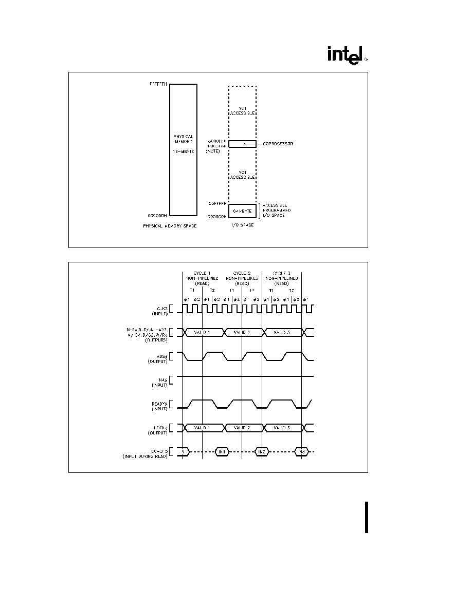
Intel386
TM
SX MICROPROCESSOR
NOTE
240187 � 18
Since A23 is HIGH during automatic communication with coprocessor A23 HIGH and M IO
LOW can be used to
easily generate a coprocessor select signal
Figure 5 3 Physical Memory and I O Spaces
240187 � 19
Fastest non-pipelined bus cycles consist of T1 and T2
Figure 5 4 Fastest Read Cycles with Non-pipelined Address Timing
46

Intel386
TM
SX MICROPROCESSOR
when the Intel386 SX Microprocessor issues a new
bus cycle definition and address
Collectively the address bus data bus and all asso-
ciated control signals are referred to simply as `the
bus' When active the bus performs one of the bus
cycles below
1 Read from memory space
2 Locked read from memory space
3 Write to memory space
4 Locked write to memory space
5 Read from I O space (or coprocessor)
6 Write to I O space (or coprocessor)
7 Interrupt acknowledge (always locked)
8 Indicate halt or indicate shutdown
Table 5 2 shows the encoding of the bus cycle defi-
nition signals for each bus cycle See Bus Cycle
Definition Signals
for additional information
When the Intel386 SX Microprocessor bus is not
performing one of the activities listed above it is ei-
ther Idle or in the Hold Acknowledge state which
may be detected externally The idle state can be
identified by the Intel386 SX Microprocessor giving
no further assertions on its address strobe output
(ADS ) since the beginning of its most recent bus
cycle and the most recent bus cycle having been
terminated The hold acknowledge state is identified
by the Intel386 SX Microprocessor asserting its hold
acknowledge (HLDA) output
The shortest time unit of bus activity is a bus state A
bus state is one processor clock period (two CLK2
periods) in duration A complete data transfer occurs
during a bus cycle composed of two or more bus
states
The fastest Intel386 SX Microprocessor bus cycle
requires only two bus states For example three
consecutive bus read cycles each consisting of two
bus states are shown by Figure 5 4 The bus states
in each cycle are named T1 and T2 Any memory or
I O address may be accessed by such a two-state
bus cycle if the external hardware is fast enough
240187 � 20
Fastest pipelined bus cycles consist of T1P and T2P
Figure 5 5 Fastest Read Cycles with Pipelined Address Timing
47

Intel386
TM
SX MICROPROCESSOR
Every bus cycle continues until it is acknowledged
by the external system hardware using the Intel386
SX Microprocessor READY
input Acknowledging
the bus cycle at the end of the first T2 results in the
shortest bus cycle requiring only T1 and T2 If
READY
is not immediately asserted however T2
states are repeated indefinitely until the READY
input is sampled active
The address pipelining option provides a choice of
bus cycle timings Pipelined or non-pipelined ad-
dress timing is selectable on a cycle-by-cycle basis
with the Next Address (NA ) input
When address pipelining is selected the address
(BHE
BLE
and A
23
� A
1
) and definition (W R
D C
M IO
and LOCK ) of the next cycle are
available before the end of the current cycle To sig-
nal their availability the Intel386 SX Microprocessor
address status output (ADS ) is asserted Figure
5 5 illustrates the fastest read cycles with pipelined
address timing
Note from Figure 5 5 the fastest bus cycles using
pipelined address require only two bus states
named T1P and T2P Therefore cycles with pipe-
lined address timing allow the same data bandwidth
as non-pipelined cycles but address-to-data access
time is increased by one T-state time compared to
that of a non-pipelined cycle
READ AND WRITE CYCLES
Data transfers occur as a result of bus cycles classi-
fied as read or write cycles During read cycles data
is transferred from an external device to the proces-
sor During write cycles data is transferred from the
processor to an external device
240187 � 21
Idle states are shown here for diagram variety only Write cycles are not always followed by an idle state An active bus
cycle can immediately follow the write cycle
Figure 5 6 Various Bus Cycles with Non-Pipelined Address (zero wait states)
48
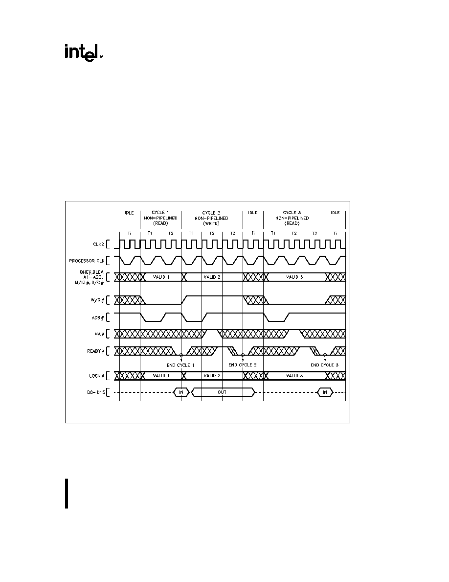
Intel386
TM
SX MICROPROCESSOR
Two choices of address timing are dynamically se-
lectable non-pipelined or pipelined After an idle bus
state the processor always uses non-pipelined ad-
dress timing However the NA
(Next Address) in-
put may be asserted to select pipelined address tim-
ing for the next bus cycle When pipelining is select-
ed and the Intel386 SX Microprocessor has a bus
request pending internally the address and defini-
tion of the next cycle is made available even before
the current bus cycle is acknowledged by READY
Terminating a read or write cycle like any bus cycle
requires acknowledging the cycle by asserting the
READY
input Until acknowledged the processor
inserts wait states into the bus cycle to allow adjust-
ment for the speed of any external device External
hardware which has decoded the address and bus
cycle type asserts the READY
input at the appro-
priate time
At the end of the second bus state within the bus
cycle READY
is sampled At that time if external
hardware acknowledges the bus cycle by asserting
READY
the bus cycle terminates as shown in Fig-
ure 5 6 If READY
is negated as in Figure 5 7 the
Intel386 SX Microprocessor executes another bus
state (a wait state) and READY
is sampled again
at the end of that state This continues indefinitely
until the cycle is acknowledged by READY
assert-
ed
When the current cycle is acknowledged
the
Intel386 SX Microprocessor terminates it When a
read cycle is acknowledged the Intel386 SX Micro-
processor latches the information present at its data
pins When a write cycle is acknowledged the
Intel386 SX CPU's write data remains valid through-
out phase one of the next bus state to provide write
data hold time
240187 � 22
Idle states are shown here for diagram variety only Write cycles are not always followed by an idle state An active bus
cycle can immediately follow the write cycle
Figure 5 7 Various Bus Cycles with Non-Pipelined Address (various number of wait states)
49
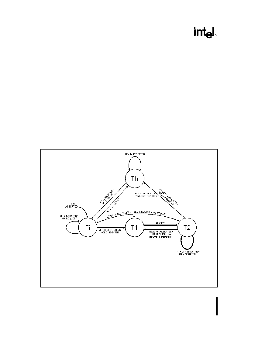
Intel386
TM
SX MICROPROCESSOR
Non-Pipelined Address
Any bus cycle may be performed with non-pipelined
address timing For example Figure 5 6 shows a
mixture of read and write cycles with non-pipelined
address timing Figure 5 6 shows that the fastest
possible cycles with non-pipelined address have two
bus states per bus cycle The states are named T1
and T2 In phase one of T1 the address signals and
bus cycle definition signals are driven valid and to
signal their availability address strobe (ADS ) is
simultaneously asserted
During read or write cycles the data bus behaves as
follows If the cycle is a read the Intel386 SX Micro-
processor floats its data signals to allow driving by
the external device being addressed The Intel386
SX Microprocessor requires that all data bus
pins be at a valid logic state (HIGH or LOW) at
the end of each read cycle when READY
is
asserted
The system MUST be designed to
meet this requirement
If the cycle is a write data
signals are driven by the Intel386 SX Microproces-
sor beginning in phase two of T1 until phase one of
the bus state following cycle acknowledgment
Figure 5 7 illustrates non-pipelined bus cycles with
one wait state added to Cycles 2 and 3 READY
is
sampled inactive at the end of the first T2 in Cycles
2 and 3 Therefore Cycles 2 and 3 have T2 repeated
again At the end of the second T2 READY
is
sampled active
When address pipelining is not used the address
and bus cycle definition remain valid during all wait
states When wait states are added and it is desir-
able to maintain non-pipelined address timing it is
necessary to negate NA
during each T2 state ex-
cept the last one as shown in Figure 5 7 Cycles 2
and 3 If NA
is sampled active during a T2 other
than the last one the next state would be T2I or T2P
instead of another T2
When address pipelining is not used the bus states
and transitions are completely illustrated by Figure
5 8
The bus transitions between four possible
states T1 T2 T
i
and T
h
Bus cycles consist of T1
and T2 with T2 being repeated for wait states Oth-
erwise the bus may be idle T
i
or in the hold ac-
knowledge state T
h
240187 � 23
Bus States
T1
first clock of a non-pipelined bus cycle (Intel386
TM
SX CPU drives new address and asserts ADS )
T2
subsequent clocks of a bus cycle when NA
has not been sampled asserted in the current bus cycle
Ti
idle state
Th
hold acknowledge state (Intel386 SX CPU asserts HLDA)
The fastest bus cycle consists of two states T1 and T2
Four basic bus states describe bus operation when not using pipelined address
Figure 5 8 Bus States (not using pipelined address)
50
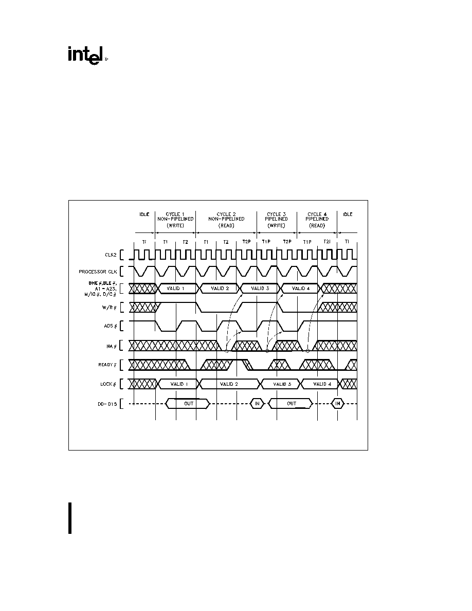
Intel386
TM
SX MICROPROCESSOR
Bus cycles always begin with T1 T1 always leads to
T2 If a bus cycle is not acknowledged during T2 and
NA
is inactive T2 is repeated When a cycle is
acknowledged during T2 the following state will be
T1 of the next bus cycle if a bus request is pending
internally or T
i
if there is no bus request pending or
T
h
if the HOLD input is being asserted
Use of pipelined address allows the Intel386 SX Mi-
croprocessor to enter three additional bus states not
shown in Figure 5 8 Figure 5 12 is the complete bus
state diagram including pipelined address cycles
Pipelined Address
Address pipelining is the option of requesting the
address and the bus cycle definition of the next in-
ternally pending bus cycle before the current bus
cycle is acknowledged with READY
asserted
ADS
is asserted by the Intel386 SX Microproces-
sor when the next address is issued The address
pipelining option is controlled on a cycle-by-cycle
basis with the NA
input signal
Once a bus cycle is in progress and the current ad-
dress has been valid for at least one entire bus
state the NA
input is sampled at the end of every
phase one until the bus cycle is acknowledged Dur-
ing non-pipelined bus cycles NA
is sampled at the
end of phase one in every T2 An example is Cycle 2
in Figure 5 9 during which NA
is sampled at the
end of phase one of every T2 (it was asserted once
during the first T2 and has no further effect during
that bus cycle)
240187 � 24
Following any idle bus state (Ti) addresses are non-pipelined Within non-pipelined bus cycles NA
is only sampled
during wait states Therefore to begin address pipelining during a group of non-pipelined bus cycles requires a non-pipe-
lined cycle with at least one wait state (Cycle 2 above)
Figure 5 9 Transitioning to Pipelined Address During Burst of Bus Cycles
51
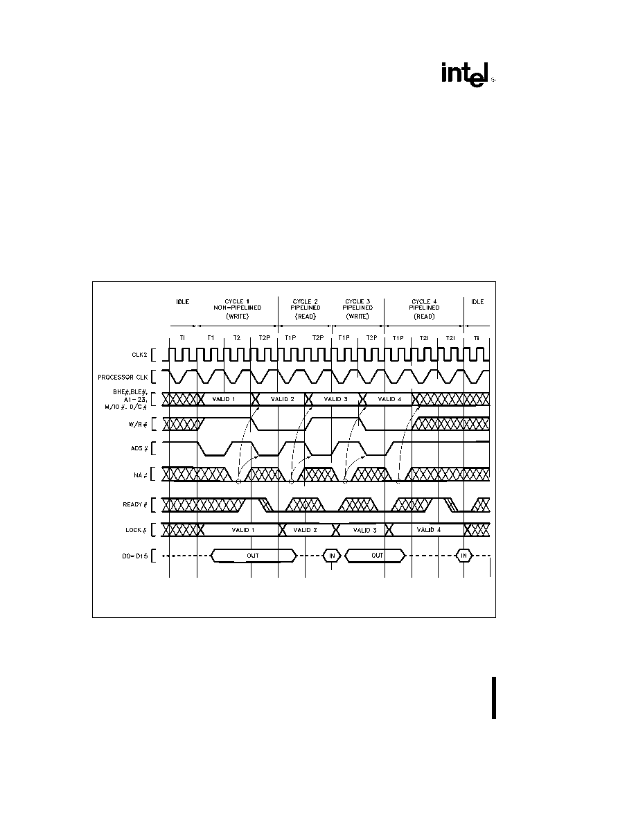
Intel386
TM
SX MICROPROCESSOR
If NA
is sampled active the Intel386 SX Micro-
processor is free to drive the address and bus cycle
definition of the next bus cycle and assert ADS
as soon as it has a bus request internally pending It
may drive the next address as early as the next bus
state whether the current bus cycle is acknowl-
edged at that time or not
Regarding the details of address pipelining the
Intel386 SX Microprocessor has the following char-
acteristics
1 The next address may appear as early as the bus
state after NA
was sampled active (see Figures
5 9 or 5 10) In that case state T2P is entered
immediately However when there is not an inter-
nal bus request already pending the next address
will not be available immediately after NA
is as-
serted and T2I is entered instead of T2P (see Fig-
ure 5 11 Cycle 3) Provided the current bus cycle
isn't yet acknowledged by READY
asserted
T2P will be entered as soon as the Intel386 SX
Microprocessor does drive the next address Ex-
ternal hardware should therefore observe the
ADS
output as confirmation the next address is
actually being driven on the bus
2 Any address which is validated by a pulse on the
ADS
output will remain stable on the address
pins for at least two processor clock periods The
Intel386 SX Microprocessor cannot produce a
new address more frequently than every two
processor clock periods (see Figures 5 9 5 10
and 5 11)
3 Only the address and bus cycle definition of the
very next bus cycle is available The pipelining ca-
pability cannot look further than one bus cycle
ahead (see Figure 5 11 Cycle 1)
240187 � 25
Following any bus state (Ti) the address is always non-pipelined and NA
is only sampled during wait states To start
address pipelining after an idle state requires a non-pipelined cycle with at least one wait state (cycle 1 above)
The pipelined cycles (2 3 4 above) are shown with various numbers of wait states
Figure 5 10 Fastest Transition to Pipelined Address Following Idle Bus State
52

Intel386
TM
SX MICROPROCESSOR
The complete bus state transition diagram including
operation with pipelined address is given by Figure
5 12 Note it is a superset of the diagram for non-
pipelined address only and the three additional bus
states for pipelined address are drawn in bold
The fastest bus cycle with pipelined address con-
sists of just two bus states T1P and T2P (recall for
non-pipelined address it is T1 and T2) T1P is the
first bus state of a pipelined cycle
240187 � 26
Figure 5 11 Details of Address Pipelining During Cycles with Wait States
53

Intel386
TM
SX MICROPROCESSOR
Bus States
T1
first clock of a non-pipelined bus cycle (Intel386
TM
SX CPU
drives new address and asserts ADS )
T2
subsequent clocks of a bus cycle when NA
has not been
sampled asserted in the current bus cycle
T2I
subsequent clocks of a bus cycle when NA
has been
sampled asserted in the current bus cycle but there is not yet
an internal bus request pending (Intel386 SX CPU will not drive
new address or assert ADS )
T2P
subsequent clocks of a bus cycle when NA
has been
sampled asserted in the current bus cycle and there is an inter-
nal bus request pending (Intel386 SX CPU drives new address
and asserts ADS )
T1P
first clock of a pipelined bus cycle
Ti
idle state
240187 � 27
Th
hold acknowledge state (Intel386 SX CPU asserts HLDA)
Asserting NA
for pipelined address gives access to three
more bus states T2I T2P and T1P
Using pipelined address the fastest bus cycle consists of T1P
and T2P
Figure 5 12 Complete Bus States (including pipelined address)
54

Intel386
TM
SX MICROPROCESSOR
Initiating and Maintaining Pipelined Address
Using the state diagram Figure 5 12 observe the
transitions from an idle state T
i
to the beginning of
a pipelined bus cycle T1P From an idle state T
i
the
first bus cycle must begin with T1 and is therefore a
non-pipelined bus cycle The next bus cycle will be
pipelined however provided NA
is asserted and
the first bus cycle ends in a T2P state (the address
for the next bus cycle is driven during T2P) The fast-
est path from an idle state to a bus cycle with pipe-
lined address is shown in bold below
T
i
T
i
T
i
T1 - T2 - T2P T1P - T2P
idle
non-pipelined
pipelined
states
cycle
cycle
T1-T2-T2P are the states of the bus cycle that es-
tablish address pipelining for the next bus cycle
which begins with T1P The same is true after a bus
hold state shown below
T
h
T
h
T
h
T1 - T2 - T2P T1P - T2P
hold acknowledge
non-pipelined
pipelined
states
cycle
cycle
The transition to pipelined address is shown func-
tionally by Figure 5 10 Cycle 1 Note that Cycle 1 is
used to transition into pipelined address timing for
the subsequent Cycles 2 3 and 4 which are pipe-
lined The NA
input is asserted at the appropriate
time to select address pipelining for Cycles 2 3 and
4
Once a bus cycle is in progress and the current ad-
dress has been valid for one entire bus state the
NA
input is sampled at the end of every phase one
until the bus cycle is acknowledged Sampling be-
gins in T2 during Cycle 1 in Figure 5 10 Once NA
is sampled active during the current cycle
the
Intel386 SX Microprocessor is free to drive a new
address and bus cycle definition on the bus as early
as the next bus state In Figure 5 10 Cycle 1 for
example the next address is driven during state
T2P Thus Cycle 1 makes the transition to pipelined
address timing since it begins with T1 but ends with
T2P Because the address for Cycle 2 is available
before Cycle 2 begins Cycle 2 is called a pipelined
bus cycle and it begins with T1P Cycle 2 begins as
soon as READY
asserted terminates Cycle 1
Examples of transition bus cycles are Figure 5 10
Cycle 1 and Figure 5 9 Cycle 2 Figure 5 10 shows
transition during the very first cycle after an idle bus
state which is the fastest possible transition into ad-
dress pipelining Figure 5 9 Cycle 2 shows a tran-
sition cycle occurring during a burst of bus cycles In
any case a transition cycle is the same whenever it
occurs it consists at least of T1 T2 (NA
is assert-
ed at that time) and T2P (provided the Intel386 SX
Microprocessor has an internal bus request already
pending which it almost always has) T2P states are
repeated if wait states are added to the cycle
Note that only three states (T1 T2 and T2P) are
required in a bus cycle performing a transition from
non-pipelined address into pipelined address timing
for example Figure 5 10 Cycle 1 Figure 5 10 Cycles
2 3 and 4 show that address pipelining can be main-
tained with two-state bus cycles consisting only of
T1P and T2P
Once a pipelined bus cycle is in progress pipelined
timing is maintained for the next cycle by asserting
NA
and detecting that the Intel386 SX Microproc-
essor enters T2P during the current bus cycle The
current bus cycle must end in state T2P for pipelin-
ing to be maintained in the next cycle T2P is identi-
fied by the assertion of ADS
Figures 5 9 and 5 10
however each show pipelining ending after Cycle 4
because Cycle 4 ends in T2I This indicates the
Intel386 SX Microprocessor didn't have an internal
bus request prior to the acknowledgement of Cycle
4 If a cycle ends with a T2 or T2I the next cycle will
not be pipelined
Realistically address pipelining is almost always
maintained as long as NA
is sampled asserted
This is so because in the absence of any other re-
quest a code prefetch request is always internally
pending until the instruction decoder and code pre-
fetch queue are completely full Therefore address
pipelining is maintained for long bursts of bus cycles
if the bus is available (i e HOLD inactive) and NA
is sampled active in each of the bus cycles
55
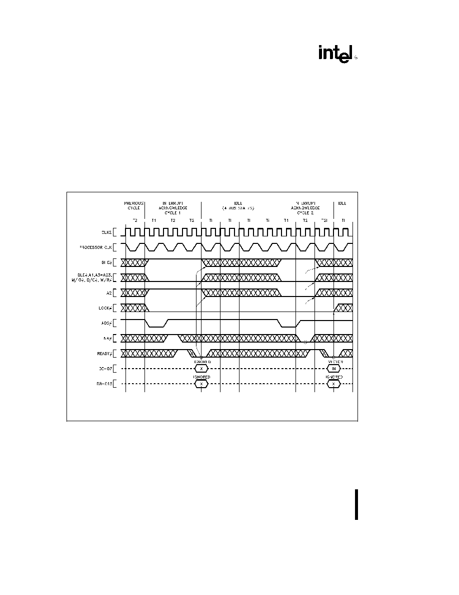
Intel386
TM
SX MICROPROCESSOR
INTERRUPT ACKNOWLEDGE (INTA) CYCLES
In response to an interrupt request on the INTR in-
put when interrupts are enabled the Intel386 SX Mi-
croprocessor performs two interrupt acknowledge
cycles These bus cycles are similar to read cycles
in that bus definition signals define the type of bus
activity taking place and each cycle continues until
acknowledged by READY
sampled active
The state of A
2
distinguishes the first and second
interrupt acknowledge cycles
The byte address
driven during the first interrupt acknowledge cycle is
4 (A
23
� A
3
A
1
BLE
LOW A
2
and BHE
HIGH)
The byte address driven during the second interrupt
acknowledge cycle is 0 (A
23
� A
1
BLE
LOW and
BHE
HIGH)
The LOCK
output is asserted from the beginning
of the first interrupt acknowledge cycle until the end
of the second interrupt acknowledge cycle Four idle
bus states T
i
are inserted by the Intel386 SX Micro-
processor between the two interrupt acknowledge
cycles for compatibility with spec TRHRL of the
8259A Interrupt Controller
During both interrupt acknowledge cycles D
15
� D
0
float No data is read at the end of the first interrupt
acknowledge cycle At the end of the second inter-
rupt acknowledge cycle the Intel386 SX Microproc-
essor will read an external interrupt vector from D
7
�
D
0
of the data bus The vector indicates the specific
interrupt number (from 0 � 255) requiring service
240187 � 28
Interrupt Vector (0 � 255) is read on D0 � D7 at end of second interrupt Acknowledge bus cycle
Because each Interrupt Acknowledge bus cycle is followed by idle bus states asserting NA
has no practical effect
Choose the approach which is simplest for your system hardware design
Figure 5 13 Interrupt Acknowledge Cycles
56

Intel386
TM
SX MICROPROCESSOR
HALT INDICATION CYCLE
The execution unit halts as a result of executing a
HLT instruction Signaling its entrance into the halt
state a halt indication cycle is performed The halt
indication cycle is identified by the state of the bus
definition signals shown on page 40 Bus Cycle
Definition Signals
and an address of 2 The halt
indication cycle must be acknowledged by READY
asserted A halted Intel386 SX Microprocessor re-
sumes execution when INTR (if interrupts are en-
abled) NMI or RESET is asserted
240187 � 29
Figure 5 14 Example Halt Indication Cycle from Non-Pipelined Cycle
57

Intel386
TM
SX MICROPROCESSOR
SHUTDOWN INDICATION CYCLE
The Intel386 SX Microprocessor shuts down as a
result of a protection fault while attempting to pro-
cess a double fault Signaling its entrance into the
shutdown state a shutdown indication cycle is per-
formed The shutdown indication cycle is identified
by the state of the bus definition signals shown in
Bus Cycle Definition Signals
and an address of 0
The shutdown indication cycle must be acknowl-
edged by READY
asserted A shutdown Intel386
SX Microprocessor resumes execution when NMI or
RESET is asserted
ENTERING AND EXITING HOLD
ACKNOWLEDGE
The bus hold acknowledge state T
h
is entered in
response to the HOLD input being asserted In the
bus hold acknowledge state the Intel386 SX Micro-
processor floats all outputs or bidirectional signals
except for HLDA HLDA is asserted as long as the
Intel386 SX Microprocessor remains in the bus hold
acknowledge state In the bus hold acknowledge
state all inputs except HOLD FLT
and RESET are
ignored
240187 � 30
Figure 5 15 Example Shutdown Indication Cycle from Non-Pipelined Cycle
58

Intel386
TM
SX MICROPROCESSOR
T
h
may be entered from a bus idle state as in Figure
5 16 or after the acknowledgement of the current
physical bus cycle if the LOCK
signal is not assert-
ed as in Figures 5 17 and 5 18
T
h
is exited in response to the HOLD input being
negated The following state will be T
i
as in Figure
5 16 if no bus request is pending The following bus
state will be T1 if a bus request is internally pending
as in Figures 5 17 and 5 18 T
h
is exited in response
to RESET being asserted
If a rising edge occurs on the edge-triggered NMI
input while in T
h
the event is remembered as a non-
maskable interrupt 2 and is serviced when T
h
is exit-
ed unless the Intel386 SX Microprocessor is reset
before T
h
is exited
RESET DURING HOLD ACKNOWLEDGE
RESET being asserted takes priority over HOLD be-
ing asserted If RESET is asserted while HOLD re-
mains asserted the Intel386 SX Microprocessor
drives its pins to defined states during reset as in
Table 5 5 Pin State During Reset
and performs
internal reset activity as usual
If HOLD remains asserted when RESET is inactive
the Intel386 SX Microprocessor enters the hold ac-
knowledge state before performing its first bus cy-
cle
provided HOLD is still asserted when the
Intel386 SX Microprocessor would otherwise per-
form its first bus cycle
240187 � 31
NOTE
For maximum design flexibility the Intel386
TM
SX CPU has no internal pullup resistors on its outputs Your design may
require an external pullup on ADS
and other outputs to keep them negated during float periods
Figure 5 16 Requesting Hold from Idle Bus
59
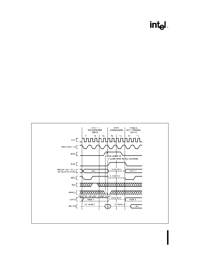
Intel386
TM
SX MICROPROCESSOR
FLOAT
Activating the FLT
input floats all Intel386 SX bidi-
rectional and output signals including HLDA Assert-
ing FLT
isolates the Intel386 SX from the sur-
rounding circuitry
As the Intel386 SX is packaged in a surface mount
PQFP it cannot be removed from the motherboard
when In-Circuit Emulation (ICE) is needed
The
FLT
input allows the Intel386 SX to be electrically
isolated from the surrounding circuitry This allows
connection of an emulator to the Intel386 SX PQFP
without removing it from the PCB This method of
emulation is referred to as ON-Circuit Emulation
(ONCE)
ENTERING AND EXITING FLOAT
FLT
is an asynchronous active-low input It is rec-
ognized on the rising edge of CLK2 When recog-
nized it aborts the current bus cycle and floats the
outputs of the Intel386 SX (Figure 5 20) FLT
must
be held low for a minimum of 16 CLK2 cycles Reset
should be asserted and held asserted until after
FLT
is deasserted
This will ensure that the
Intel386 SX will exit float in a valid state
Asserting the FLT
input unconditionally aborts the
current bus cycle and forces the Intel386 SX into the
FLOAT mode Since activating FLT
unconditional-
ly forces the Intel386 SX into FLOAT mode the
Intel386 SX is not guaranteed to enter FLOAT in a
valid state After deactivating FLT
the Intel386 SX
is not guaranteed to exit FLOAT mode in a valid
state This is not a problem as the FLT
pin is
meant to be used only during ONCE After exiting
FLOAT the Intel386 SX must be reset to return it to
a valid state Reset should be asserted before FLT
is deasserted This will ensure that the Intel386 SX
will exit float in a valid state
FLT
has an internal pull-up resistor and if it is not
used it should be unconnected
BUS ACTIVITY DURING AND FOLLOWING
RESET
RESET is the highest priority input signal capable of
interrupting any processor activity when it is assert-
ed A bus cycle in progress can be aborted at any
stage or idle states or bus hold acknowledge states
discontinued so that the reset state is established
240187 � 32
NOTE
HOLD is a synchronous input and can be asserted at any CLK2 edge provided setup and hold (t
23
and t
24
) require-
ments are met This waveform is useful for determining Hold Acknowledge latency
Figure 5 17 Requesting Hold from Active Bus (NA
inactive)
60

Intel386
TM
SX MICROPROCESSOR
RESET should remain asserted for at least 15 CLK2
periods to ensure it is recognized throughout the
Intel386 SX Microprocessor and at least 80 CLK2
periods if self-test is going to be requested at the
falling edge RESET asserted pulses less than 15
CLK2 periods may not be recognized RESET puls-
es less than 80 CLK2 periods followed by a self-test
may cause the self-test to report a failure when no
true failure exists
Provided the RESET falling edge meets setup and
hold times t
25
and t
26
the internal processor clock
phase is defined at that time as illustrated by Figure
5 19 and Figure 7 7
A self-test may be requested at the time RESET
goes inactive by having the BUSY
input at a LOW
level as shown in Figure 5 19 The self-test requires
approximately (2
20
a
60) CLK2 periods to com-
plete The self-test duration is not affected by the
test results Even if the self-test indicates a problem
the Intel386 SX Microprocessor attempts to proceed
with the reset sequence afterwards
After the RESET falling edge (and after the self-test
if it was requested) the Intel386 SX Microprocessor
performs an internal initialization sequence for ap-
proximately 350 to 450 CLK2 periods
240187 � 33
NOTE
HOLD is a synchronous input and can be asserted at any CLK2 edge provided setup and hold (t23 and t24) require-
ments are met This waveform is useful for determining Hold Acknowledge latency
Figure 5 18 Requesting Hold from Idle Bus (NA
active)
61
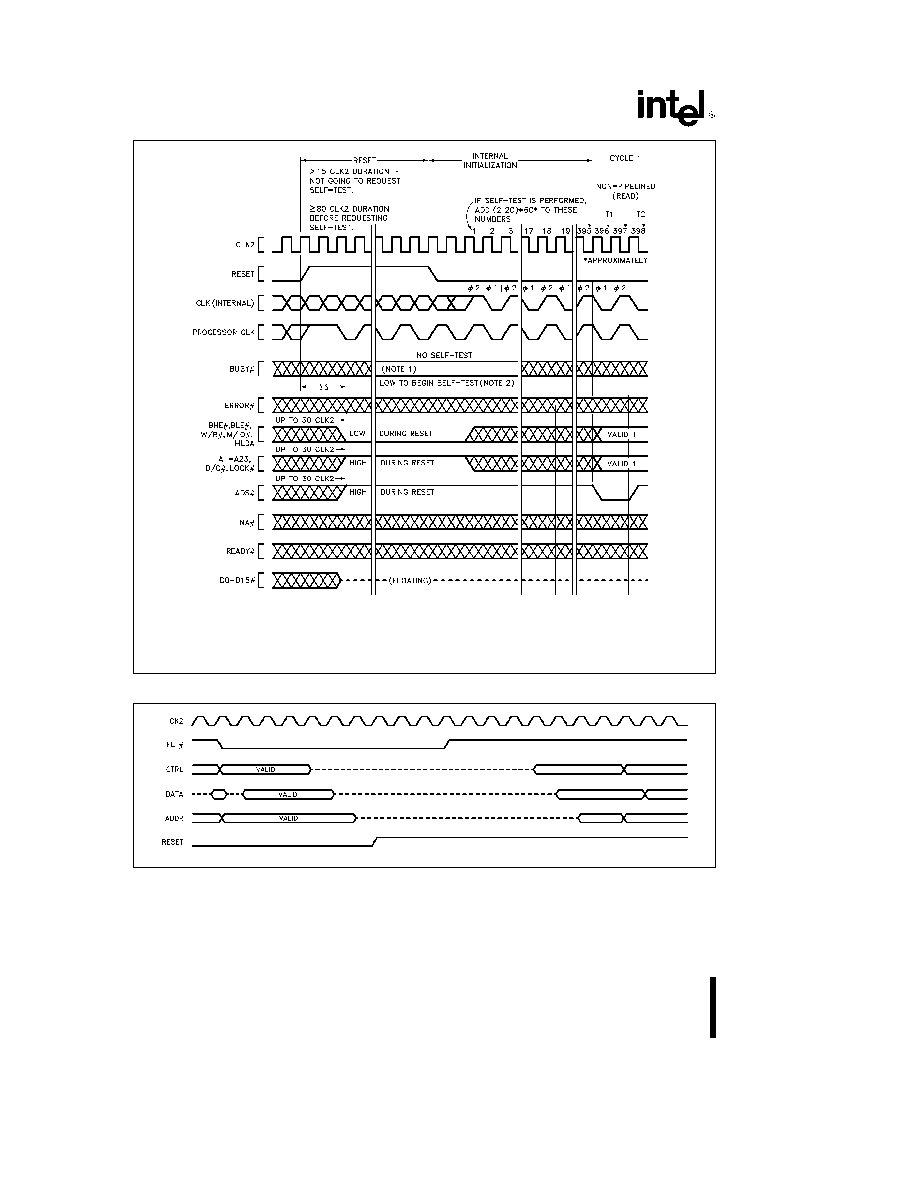
Intel386
TM
SX MICROPROCESSOR
240187 � 34
NOTES
1 BUSY
should be held stable for 8 CLK2 periods before and after the CLK2 period in which RESET falling edge
occurs
2 If self-test is requested the outputs remain in their reset state as shown here
Figure 5 19 Bus Activity from Reset Until First Code Fetch
240187 � 51
Figure 5 20 Entering and Exiting FLT
62
Intel386
TM
SX MICROPROCESSOR
5 5 Self-test Signature
Upon completion of self-test (if self-test was re-
quested by driving BUSY
LOW at the falling edge
of RESET) the EAX register will contain a signature
of 00000000H indicating the Intel386 SX Microproc-
essor passed its self-test of microcode and major
PLA contents with no problems detected The pass-
ing signature in EAX 00000000H applies to all revi-
sion levels Any non-zero signature indicates the unit
is faulty
5 6 Component and Revision
Identifiers
To assist users the Intel386 SX Microprocessor af-
ter reset holds a component identifier and revision
identifier in its DX register The upper 8 bits of DX
hold 23H as identification of the Intel386 SX Micro-
processor (the lower nibble 03H refers to the
Intel386 DX Architecture The upper nibble 02H re-
fers to the second member of the Intel386 DX Fami-
ly) The lower 8 bits of DX hold an 8-bit unsigned
binary number related to the component revision
level The revision identifier will in general chrono-
logically track those component steppings which are
intended to have certain improvements or distinction
from previous steppings The Intel386 SX Microproc-
essor revision identifier will track that of the Intel386
DX CPU where possible
The revision identifier is intended to assist users to a
practical extent However the revision identifier val-
ue is not guaranteed to change with every stepping
revision or to follow a completely uniform numerical
sequence depending on the type or intention of re-
vision or manufacturing materials required to be
changed Intel has sole discretion over these char-
acteristics of the component
Table 5 7 Component and
Revision Identifier History
Stepping
Revision Identifier
A0
04H
B
05H
C
08H
D
08H
E
08H
5 7 Coprocessor Interfacing
The Intel386 SX Microprocessor provides an auto-
matic interface for the Intel Intel387 SX numeric
floating-point coprocessor The Intel387 SX coproc-
essor uses an I O mapped interface driven automat-
ically by the Intel386 SX Microprocessor and assist-
ed by three dedicated signals BUSY
ERROR
and PEREQ
As the Intel386 SX Microprocessor begins support-
ing a coprocessor instruction it tests the BUSY
and ERROR
signals to determine if the coproces-
sor can accept its next instruction
Thus
the
BUSY
and ERROR
inputs eliminate the need for
any `preamble' bus cycles for communication be-
tween processor and coprocessor The Intel387 SX
can be given its command opcode immediately The
dedicated signals provide instruction synchroniza-
tion and eliminate the need of using the WAIT op-
code (9BH) for Intel387 SX instruction synchroniza-
tion (the WAIT opcode was required when the 8086
or 8088 was used with the 8087 coprocessor)
Custom coprocessors can be included in Intel386
SX Microprocessor based systems by memory-
mapped or I O-mapped interfaces Such coproces-
sor interfaces allow a completely custom protocol
and are not limited to a set of coprocessor protocol
`primitives'
Instead
memory-mapped
or
I O-
mapped interfaces may use all applicable instruc-
tions for high-speed coprocessor communication
The BUSY
and ERROR
inputs of the Intel386
SX Microprocessor may also be used for the custom
coprocessor interface if such hardware assist is de-
sired These signals can be tested by the WAIT op-
code (9BH) The WAIT instruction will wait until the
BUSY
input is inactive (interruptable by an NMI or
enabled INTR input) but generates an exception 16
fault if the ERROR
pin is active when the BUSY
goes (or is) inactive If the custom coprocessor inter-
face is memory-mapped protection of the address-
es used for the interface can be provided with the
Intel386 SX CPU's on-chip paging or segmentation
mechanisms If the custom interface is I O-mapped
protection of the interface can be provided with the
IOPL (I O Privilege Level) mechanism
The Intel387 SX numeric coprocessor interface is
I O mapped as shown in Table 5 8 Note that the
Intel387 SX coprocessor interface addresses are
beyond the 0H-0FFFFH range for programmed I O
When the Intel386 SX Microprocessor supports the
Intel387 SX coprocessor the Intel386 SX Micro-
processor automatically generates bus cycles to the
coprocessor interface addresses
Table 5 8 Numeric Coprocessor Port Addresses
Address in Intel386 SX
Intel387 SX
CPU I O Space
Coprocessor Register
8000F8H
Opcode Register
8000FCH 8000FEH
Operand Register
Generated as 2nd bus cycle during Dword transfer
To correctly map the Intel387 SX registers to the
appropriate I O addresses connect the CMD0 and
CMD1 lines of the Intel387 SX as listed in Table 5 9
Table 5 9 Connections for CMD0
and CMD1 Inputs for the Intel387 SX
Signal
Connection
CMD0
Connect directly
to Intel386 SX CPU A2 signal
CMD1
Connect to ground
63

Intel386
TM
SX MICROPROCESSOR
Software Testing for Coprocessor Presence
When software is used to test for coprocessor
(Intel387 SX) presence it should use only the follow-
ing coprocessor opcodes FINIT FNINIT FSTCW
mem FSTSW mem and FSTSW AX To use other
coprocessor opcodes when a coprocessor is known
to be not present first set EM e 1 in the Intel386 SX
CPU's CR0 register
6 0 PACKAGE THERMAL
SPECIFICATIONS
The Intel386 SX Microprocessor is specified for op-
eration when case temperature (T
c
) is within the
range of 0 C � 100 C The case temperature may be
measured in any environment to determine whether
the Intel386 SX Microprocessor is within specified
operating range The case temperature should be
measured at the center of the top surface opposite
the pins
The ambient temperature (T
a
) is related to T
c
and
the thermal conductivity parameters i
ja
and i
jc
from
the following equations (eqn 3 is derived by elimi-
nating the junction temperature (T
j
) between eqns
1 and 2)
1) T
j
e
T
c
a
P i
jc
2) T
a
e
T
j
b
P i
ja
3) T
c
e
T
a
a
P i
ja
b
i
jc
Values for i
ja
and i
jc
are given in Table 6 1 for the
100 lead fine pitch i
ja
is given at various airflows
The power (P) dissipated by the chip as heat is
Vcc Icc A guaranteed maximum safe T
a
can be cal-
culated from eqn 3 by using the maximum safe T
c
of
100 C along with the maximum power drawn by the
chip in the given design and i
jc
and i
ja
values from
Table 6 1 (The i
ja
value depends on the airflow
measured at the top of the chip provided by the
system ventilation )
7 0 ELECTRICAL SPECIFICATIONS
The following sections describe recommended elec-
trical connections for the Intel386 SX Microproces-
sor and its electrical specifications
7 1 Power and Grounding
The Intel386 SX Microprocessor is implemented in
CHMOS IV technology and has modest power re-
quirements However its high clock frequency and
47 output buffers (address data control and HLDA)
can cause power surges as multiple output buffers
drive new signal levels simultaneously For clean on-
chip power distribution at high frequency 14 Vcc
and 18 Vss pins separately feed functional units of
the Intel386 SX Microprocessor
Power and ground connections must be made to all
external Vcc and Vss pins of the Intel386 SX Micro-
processor On the circuit board all Vcc pins should
be connected on a Vcc plane and all Vss pins
should be connected on a GND plane
POWER DECOUPLING RECOMMENDATIONS
Liberal decoupling capacitors should be placed near
the Intel386 SX Microprocessor The Intel386 SX Mi-
croprocessor driving its 24-bit address bus and
16-bit data bus at high frequencies can cause tran-
sient power surges particularly when driving large
capacitive loads Low inductance capacitors and in-
terconnects are recommended for best high fre-
quency electrical performance Inductance can be
reduced by shortening circuit board traces between
the Intel386 SX Microprocessor and decoupling ca-
pacitors as much as possible
Table 6 1 Thermal Resistances ( C Watt) i
jc
and i
ja
i
ja
versus Airflow - ft min (m sec)
Package
i
jc
0
200
400
600
800
1000
(0)
(1 01)
(2 03)
(3 04)
(4 06)
(5 07)
100 Lead
7 5
34 5
29 5
25 5
22 5
21 5
21
Fine Pitch
64

Intel386
TM
SX MICROPROCESSOR
Table 7 1 Recommended Resistor Pull-ups to Vcc
Pin
Signal
Pull-up Value
Purpose
16
ADS
20 KX
g
10%
Lightly pull ADS
inactive during
Intel386
TM
SX CPU hold acknowledge
states
26
LOCK
20 KX
g
10%
Lightly pull LOCK
inactive during
Intel386
TM
SX CPU hold acknowledge
states
RESISTOR RECOMMENDATIONS
The ERROR
FLT
and BUSY
inputs have inter-
nal pull-up resistors of approximately 20 KX and the
PEREQ input has an internal pull-down resistor of
approximately 20 KX built into the Intel386 SX Mi-
croprocessor to keep these signals inactive when
the Intel387 SX is not present in the system (or tem-
porarily removed from its socket)
In typical designs
the external pull-up resistors
shown in Table 7 1 are recommended However a
particular design may have reason to adjust the re-
sistor values recommended here or alter the use of
pull-up resistors in other ways
OTHER CONNECTION RECOMMENDATIONS
For reliable operation always connect unused in-
puts to an appropriate signal level N C pins should
always remain unconnected Connection of N C
pins to Vcc or Vss will result in component mal-
function or incompatibility with future steppings
of the Intel386 SX Microprocessor
Particularly when not using interrupts or bus hold (as
when first prototyping) prevent any chance of spuri-
ous activity by connecting these associated inputs to
GND
Pin
Signal
40
INTR
38
NMI
4
HOLD
If not using address pipelining connect pin 6 NA
through a pull-up in the range of 20 KX to Vcc
7 2 Maximum Ratings
Table 7 2 Maximum Ratings
Parameter
Maximum Rating
Storage temperature
b
65 C to 150 C
Case temperature under bias
b
65 C to 110 C
Supply voltage with respect
to Vss
b
5V to 6 5V
Voltage on other pins
b
5V to (Vcca 5)V
Table 7 2 gives stress ratings only and functional
operation at the maximums is not guaranteed Func-
tional operating conditions are given in section 7 3
D C Specifications
and section 7 4 A C Specifi-
cations
Extended exposure to the Maximum Ratings may af-
fect device reliability
Furthermore
although the
Intel386 SX Microprocessor contains protective cir-
cuitry to resist damage from static electric discharge
always take precautions to avoid high static voltages
or electric fields
65

Intel386
TM
SX MICROPROCESSOR
7 3 D C Specifications
Functional operating range V
CC
e
5V
g
10% T
CASE
e
0 C to 100 C
Table 7 3 Intel386
TM
SX Microprocessor D C Characteristics
33 MHz 25 MHz 20 MHz and 16 MHz
Symbol
Parameter
Min
Max
Unit
Test Condition
V
IL
Input LOW Voltage
b
0 3
a
0 8
V
V
IH
Input HIGH Voltage
2 0
V
CC
a
0 3
V
V
ILC
CLK2 Input LOW Voltage
b
0 3
a
0 8
V
V
IHC
CLK2 Input HIGH Voltage
V
CC
b
0 8
V
CC
a
0 3
V
V
OL
Output LOW Voltage
I
OL
e
4 mA
A
23
� A
1
D
15
� D
0
0 45
V
I
OL
e
5 mA
BHE
BLE
W R
D C
0 45
V
M IO
LOCK
ADS
HLDA
V
OH
Output HIGH Voltage
I
OH
e b
1 mA
A
23
� A
1
D
15
� D
0
2 4
V
I
OH
e b
0 2 mA
A
23
� A
1
D
15
� D
0
V
CC
b
0 5
V
I
OH
e b
0 9 mA
BHE
BLE
W R
2 4
V
D C
M IO
LOCK
ADS
HLDA
I
OH
e b
0 18 mA
BHE
BLE
W R
V
CC
b
0 5
V
D C
M IO
LOCK
ADS
HLDA
I
LI
Input Leakage Current
g
15
m
A
0V
s
V
IN
s
V
CC
(for all pins except PEREQ BUSY
FLT
and ERROR )
I
IH
Input Leakage Current
200
m
A
V
IH
e
2 4V Note 1
(PEREQ pin)
I
IL
Input Leakage Current
b
400
m
A
V
IL
e
0 45V Note 2
(BUSY
ERROR
and FLT
pins)
I
LO
Output Leakage Current
g
15
m
A
0 45V
s
V
OUT
s
V
CC
I
CC
Supply Current
(See Note 3)
CLK2e32 MHz with 16 MHz Intel386 SX CPU
220
mA
I
CC
type150 mA
CLK2e40 MHz with 20 MHz Intel386 SX CPU
250
mA
I
CC
type180 mA
CLK2e50 MHz with 25 MHz Intel386 SX CPU
280
mA
I
CC
type210 mA
CLK2e66 MHz with 33 MHz Intel386 SX CPU
380
mA
I
CC
type290 mA
C
IN
Input Capacitance
10
pF
F
C
e
1 MHz Note 4
C
OUT
Output or I O Capacitance
12
pF
F
C
e
1 MHz Note 4
C
CLK
CLK2 Capacitance
20
pF
F
C
e
1 MHz Note 4
All values except I
CC
tested at the minimum operating frequency of the part (CLK2
e
8 MHz)
NOTES
1 PEREQ input has an internal pull-down resistor
2 BUSY
FLT
and ERROR
inputs each have an internal pull-up resistor
3 I
CC
max measurement at worst case frequency V
CC
and temperature with 50 pF output load
4 Not 100% tested
66

Intel386
TM
SX MICROPROCESSOR
Functional operating range V
CC
e
5V
g
10% T
CASE
e
0 C to 100 C
Table 7 4 Low Power (LP) Intel386
TM
SX Microprocessor
D C Characteristics
33 MHz 25 MHz 20 MHz 16 MHz and 12 MHz
Symbol
Parameter
Min
Max
Unit
Test Condition
V
IL
Input LOW Voltage
b
0 3
a
0 8
V
V
IH
Input HIGH Voltage
2 0
V
CC
a
0 3
V
V
ILC
CLK2 Input LOW Voltage
b
0 3
a
0 8
V
V
IHC
CLK2 Input HIGH Voltage
V
CC
b
0 8
V
CC
a
0 3
V
V
OL
Output LOW Voltage
I
OL
e
4 mA
A
23
� A
1
D
15
� D
0
0 45
V
I
OL
e
5 mA
BHE
BLE
W R
D C
0 45
V
M IO
LOCK
ADS
HLDA
V
OH
Output HIGH Voltage
I
OH
e b
1 mA
A
23
� A
1
D
15
� D
0
2 4
V
I
OH
e b
0 2 mA
A
23
� A
1
D
15
� D
0
V
CC
b
0 5
V
I
OH
e b
0 9 mA
BHE
BLE
W R
2 4
V
D C
M IO
LOCK
ADS
HLDA
I
OH
e b
0 18 mA
BHE
BLE
W R
V
CC
b
0 5
V
D C
M IO
LOCK
ADS
HLDA
I
LI
Input Leakage Current
g
15
m
A
0V
s
V
IN
s
V
CC
(for all pins except PEREQ BUSY
FLT
and ERROR )
I
IH
Input Leakage Current
200
m
A
V
IH
e
2 4V Note 1
(PEREQ pin)
I
IL
Input Leakage Current
b
400
m
A
V
IL
e
0 45V Note 2
(BUSY
ERROR
and FLT
pins)
I
LO
Output Leakage Current
g
15
m
A
0 45V
s
V
OUT
s
V
CC
I
CC
Supply Current
(See Note 3)
CLK2e4 MHz
100
mA
I
CC
type50 mA
CLK2e24 MHz with 12 MHz Intel386 SX CPU
190
mA
I
CC
type120 mA
CLK2e32 MHz with 16 MHz Intel386 SX CPU
220
mA
I
CC
type150 mA
CLK2e40 MHz with 20 MHz Intel386 SX CPU
250
mA
I
CC
type180 mA
CLK2e50 MHz with 25 MHz Intel386 SX CPU
280
mA
I
CC
type210 mA
CLK2e66 MHz with 33 MHz Intel386 SX CPU
380
mA
I
CC
type290 mA
C
IN
Input Capacitance
10
pF
F
C
e
1 MHz Note 4
C
OUT
Output or I O Capacitance
12
pF
F
C
e
1 MHz Note 4
C
CLK
CLK2 Capacitance
20
pF
F
C
e
1 MHz Note 4
All values except I
CC
tested at the minimum operating frequency of the part (CLK2
e
4 MHz)
NOTES
1 PEREQ input has an internal pull-down resistor
2 BUSY
FLT
and ERROR
inputs each have an internal pull-up resistor
3 I
CC
max measurement at worst case frequency V
CC
and temperature with 50 pF output load
4 Not 100% tested
67

Intel386
TM
SX MICROPROCESSOR
7 4 A C Specifications
The A C specifications given in Tables 7 5 through
7 8 consist of output delays input setup require-
ments and input hold requirements All A C specifi-
cations are relative to the CLK2 rising edge crossing
the 2 0V level
A C spec measurement is defined by Figure 7 1 In-
puts must be driven to the voltage levels indicated
by Figure 7 1 when A C specifications are mea-
sured Output delays are specified with minimum
and maximum limits measured as shown The mini-
mum delay times are hold times provided to external
circuitry Input setup and hold times are specified
as minimums defining the smallest acceptable sam-
pling window Within the sampling window a syn-
chronous input signal must be stable for correct op-
eration
Outputs ADS
W R
D C
M IO
LOCK
BHE
BLE
A
23
� A
1
and HLDA only change at
the beginning of phase one D
15
� D
0
(write cycles)
only change at the beginning of phase two The
READY
HOLD
BUSY
ERROR
PEREQ
FLT
and D
15
� D
0
(read cycles) inputs are sampled
at the beginning of phase one The NA
INTR and
NMI inputs are sampled at the beginning of phase
two
240187 � 35
LEGEND
A
Maximum Output Delay Spec
B
Minimum Output Delay Spec
C
Minimum Input Setup Spec
D
Minimum Input Hold Spec
Figure 7 1 Drive Levels and Measurement Points for A C Specifications
68

Intel386
TM
SX MICROPROCESSOR
A C SPECIFICATIONS
Functional operating range V
CC
e
5V
g
10% T
CASE
e
0 C to 100 C
Table 7 5 Intel386
TM
SX Microprocessor A C Characteristics
33 MHz and 25 MHz
Symbol
Parameter
33 MHz
25 MHz
Unit
Figure
Notes
Intel386 SX
Intel386 SX
Min
Max
Min
Max
Operating Frequency
4
33
4
25
MHz
Half CLK2 Frequency
t
1
CLK2 Period
15
125
20
125
ns
7 3
t
2a
CLK2 HIGH Time
6 25
7
ns
7 3
at 2V
(3)
t
2b
CLK2 HIGH Time
4 0
4
ns
7 3
at (V
CC
b
0 8)V
(3)
Note 3
t
3a
CLK2 LOW Time
6 25
7
ns
7 3
at 2V
(3)
t
3b
CLK2 LOW Time
4 5
5
ns
7 3
at 0 8V
(3)
t
4
CLK2 Fall Time
4
7
ns
7 3
(V
CC
b
0 8)V to 0 8V
(3)
t
5
CLK2 Rise Time
4
7
ns
7 3
0 8V to (V
CC
b
0 8)V
(3)
t
6
A
23
� A
1
Valid Delay
4
15
4
17
ns
7 5
C
L
e
50 pF
(4)
t
7
A
23
� A
1
Float Delay
4
20
4
30
ns
7 6
(Note 1)
t
8
BHE
BLE
LOCK
4
15
4
17
ns
7 5
C
L
e
50 pF
(4)
Valid Delay
t
9
BHE
BLE
LOCK
4
20
4
30
ns
7 6
(Note 1)
Float Delay
t
10
W R
M IO
D C
4
15
4
17
ns
7 5
C
L
e
50 pF
(4)
ADS
Valid Delay
t
11
W R
M IO
D C
4
20
4
30
ns
7 6
(Note 1)
ADS
Float Delay
t
12
D
15
� D
0
Write Data
7
23
7
23
ns
7 5
C
L
e
50 pF
(4 5)
Valid Delay
t
12a
D
15
� D
0
Write Data
2
2
ns
C
L
e
50 pF
(4)
Hold Time
t
13
D
15
� D
0
Write Data
4
17
4
22
ns
7 6
(Note 1)
Float Delay
t
14
HLDA Valid Delay
4
20
4
22
ns
7 6
C
L
e
75 pF
(4)
t
15
NA
Setup Time
5
5
ns
7 4
t
16
NA
Hold Time
2
3
ns
7 4
t
19
READY
Setup Time
7
9
ns
7 4
t
20
READY
Hold Time
4
4
ns
7 4
t
21
D
15
� D
0
Read Data
5
7
ns
7 4
Setup Time
t
22
D
15
� D
0
Read Data
3
5
ns
7 4
Hold Time
69

Intel386
TM
SX MICROPROCESSOR
Functional operating range V
CC
e
5V
g
10% T
CASE
e
0 C to 100 C
Table 7 5 Intel386
TM
SX Microprocessor A C Characteristics
33 MHz and 25 MHz
(Continued)
Symbol
Parameter
33 MHz
25 MHz
Unit
Figure
Notes
Intel386 SX
Intel386 SX
Min
Max
Min
Max
t
23
HOLD Setup Time
9
9
ns
7 4
t
24
HOLD Hold Time
2
3
ns
7 4
t
25
RESET Setup Time
5
8
ns
7 7
t
26
RESET Hold Time
2
3
ns
7 7
t
27
NMI INTR Setup Time
5
6
ns
7 4
(Note 2)
t
28
NMI INTR Hold Time
5
6
ns
7 4
(Note 2)
t
29
PEREQ ERROR
BUSY
5
6
ns
7 4
(Note 2)
FLT
Setup Time
t
30
PEREQ ERROR
BUSY
4
5
ns
7 4
(Note 2)
FLT
Hold Time
NOTES
1 Float condition occurs when maximum output current becomes less than I
LO
in magnitude Float delay is not 100%
tested
2 These inputs are allowed to be asynchronous to CLK2 The setup and hold specifications are given for testing purposes
to assure recognition within a specific CLK2 period
3 These are not tested They are guaranteed by design characterization
4 Tested with CL set at 50 pF See Figures 7 and 8 for load capacitance derating curve
5 Minimum time not 100% tested
Table 7 6 Low Power (LP) Intel386
TM
SX Microprocessor A C Characteristics
33 MHz and 25 MHz
Symbol
Parameter
33 MHz
25 MHz
Unit
Figure
Notes
Intel386 SX
Intel386 SX
Min
Max
Min
Max
Operating Frequency
2
33
2
25
MHz
Half CLK2 Frequency
t
1
CLK2 Period
15
250
20
250
ns
7 3
t
2a
CLK2 HIGH Time
6 25
7
ns
7 3
at 2V
(3)
t
2b
CLK2 HIGH Time
4 0
4
ns
7 3
at (V
CC
b
0 8)V
(3)
Note 3
t
3a
CLK2 LOW Time
6 25
7
ns
7 3
at 2V
(3)
t
3b
CLK2 LOW Time
4 5
5
ns
7 3
at 0 8V
(3)
t
4
CLK2 Fall Time
4
7
ns
7 3
(V
CC
b
0 8)V to 0 8V
(3)
t
5
CLK2 Rise Time
4
7
ns
7 3
0 8V to (V
CC
b
0 8)V
(3)
t
6
A
23
� A
1
Valid Delay
4
15
4
17
ns
7 5
C
L
e
50 pF
(4)
t
7
A
23
� A
1
Float Delay
4
20
4
30
ns
7 6
(Note 1)
t
8
BHE
BLE
LOCK
4
15
4
17
ns
7 5
C
L
e
50 pF
(4)
Valid Delay
t
9
BHE
BLE
LOCK
4
20
4
30
ns
7 6
(Note 1)
Float Delay
70

Intel386
TM
SX MICROPROCESSOR
Functional operating range V
CC
e
5V
g
10% T
CASE
e
0 C to 100 C
Table 7 6 Low Power (LP) Intel386
TM
SX Microprocessor
A C Characteristics
33 MHz and 25 MHz
(Continued)
Symbol
Parameter
33 MHz
25 MHz
Unit
Figure
Notes
Intel386 SX
Intel386 SX
Min
Max
Min
Max
t
10
W R
M IO
D C
4
15
4
17
ns
7 5
C
L
e
50 pF
(4)
ADS
Valid Delay
t
11
W R
M IO
D C
4
20
4
30
ns
7 6
(Note 1)
ADS
Float Delay
t
12
D
15
� D
0
Write Data
7
23
7
23
ns
7 5
C
L
e
50 pF
(4 5)
Valid Delay
t
12a
D
15
� D
0
Write Data
2
2
ns
C
L
e
50 pF
(4)
Hold Time
t
13
D
15
� D
0
Write Data
4
17
4
22
ns
7 6
(Note 1)
Float Delay
t
14
HLDA Valid Delay
4
20
4
22
ns
7 6
C
L
e
50 pF
(4)
t
15
NA
Setup Time
5
5
ns
7 4
t
16
NA
Hold Time
2
3
ns
7 4
t
19
READY
Setup Time
7
9
ns
7 4
t
20
READY
Hold Time
4
4
ns
7 4
t
21
D
15
� D
0
Read Data
5
7
ns
7 4
Setup Time
t
22
D
15
� D
0
Read Data
3
5
ns
7 4
Hold Time
t
23
HOLD Setup Time
9
9
ns
7 4
t
24
HOLD Hold Time
2
3
ns
7 4
t
25
RESET Setup Time
5
8
ns
7 7
t
26
RESET Hold Time
2
3
ns
7 7
t
27
NMI INTR Setup Time
5
6
ns
7 4
(Note 2)
t
28
NMI INTR Hold Time
5
6
ns
7 4
(Note 2)
t
29
PEREQ ERROR
BUSY
5
6
ns
7 4
(Note 2)
FLT
Setup Time
t
30
PEREQ ERROR
BUSY
4
5
ns
7 4
(Note 2)
FLT
Hold Time
NOTES
1 Float condition occurs when maximum output current becomes less than I
LO
in magnitude Float delay is not 100%
tested
2 These inputs are allowed to be asynchronous to CLK2 The setup and hold specifications are given for testing purposes
to assure recognition within a specific CLK2 period
3 These are not tested They are guaranteed by design characterization
4 Tested with CL set at 50 pF See Figures 7 and 8 for load capacitance derating curve
5 Minimum time not 100% tested
71
Intel386
TM
SX MICROPROCESSOR
Functional operating range V
CC
e
5V
g
10% T
CASE
e
0 C to 100 C
Table 7 7 Intel386
TM
SX A C Characteristics
20 MHz and 16 MHz
Symbol
Parameter
20 MHz
16 MHz
Unit
Figure
Notes
Intel386 SX
Intel386 SX
Min
Max
Min
Max
Operating Frequency
4
20
4
16
MHz
Half CLK2 Frequency
t
1
CLK2 Period
25
125
31
125
ns
7 3
t
2a
CLK2 HIGH Time
8
9
ns
7 3
at 2V
(3)
t
2b
CLK2 HIGH Time
5
5
ns
7 3
at (V
CC
b
0 8)V
(3)
t
3a
CLK2 LOW Time
8
9
ns
7 3
at 2V
(3)
t
3b
CLK2 LOW Time
6
7
ns
7 3
at 0 8V
(3)
t
4
CLK2 Fall Time
8
8
ns
7 3
(V
CC
b
0 8)V to 0 8V
(3)
t
5
CLK2 Rise Time
8
8
ns
7 3
0 8V to (V
CC
b
0 8)V
(3)
t
6
A
23
� A
1
Valid Delay
4
30
4
36
ns
7 5
C
L
e
120 pF
(4)
t
7
A
23
� A
1
Float Delay
4
32
4
40
ns
7 6
(Note 1)
t
8
BHE
BLE
LOCK
4
30
4
36
ns
7 5
C
L
e
75 pF
(4)
Valid Delay
t
9
BHE
BLE
LOCK
4
32
4
40
ns
7 6
(Note 1)
Float Delay
t
10a
M IO
D C
Valid Delay
6
28
6
33
ns
7 5
C
L
e
75 pF
(4)
t
10b
W R
ADS
Valid Delay
26
t
11
W R
M IO
D C
6
30
6
35
ns
7 6
(Note 1)
ADS
Float Delay
t
12
D
15
� D
0
Write Data
4
38
4
40
ns
7 5
C
L
e
120 pF
(4)
Valid Delay
t
13
D
15
� D
0
Write Data
4
27
4
35
ns
7 6
(Note 1)
Float Delay
t
14
HLDA Valid Delay
4
28
4
33
ns
7 5
C
L
e
75 pF
(4)
t
15
NA
Setup Time
5
5
ns
7 4
t
16
NA
Hold Time
12
21
ns
7 4
t
19
READY
Setup Time
12
19
ns
7 4
t
20
READY
Hold Time
4
4
ns
7 4
t
21
D
15
� D
0
Read Data
9
9
ns
7 4
Setup Time
t
22
D
15
� D
0
Read Data
6
6
ns
7 4
Hold Time
t
23
HOLD Setup Time
17
26
ns
7 4
t
24
HOLD Hold Time
5
5
ns
7 4
t
25
RESET Setup Time
12
13
ns
7 7
t
26
RESET Hold Time
4
4
ns
7 7
72

Intel386
TM
SX MICROPROCESSOR
Functional operating range V
CC
e
5V
g
10% T
CASE
e
0 C to 100 C
Table 7 7 Intel386
TM
SX A C Characteristics
20 MHz and 16 MHz
(Continued)
Symbol
Parameter
20 MHz
16 MHz
Unit
Figure
Notes
Intel386 SX
Intel386 SX
Min
Max
Min
Max
t
27
NMI INTR Setup Time
16
16
ns
7 4
(Note 2)
t
28
NMI INTR Hold Time
16
16
ns
7 4
(Note 2)
t
29
PEREQ ERROR
BUSY
14
16
ns
7 4
(Note 2)
FLT
Setup Time
t
30
PEREQ ERROR
BUSY
5
5
ns
7 4
(Note 2)
FLT
Hold Time
Table 7 8 Low Power (LP) Intel386
TM
SX A C Characteristics
20 MHz 16 MHz and 12 MHz
Symbol
Parameter
20 MHz
16 MHz
12 MHz
Unit Figure
Notes
Intel386 SX Intel386 SX Intel386 SX
Min
Max
Min
Max
Min
Max
Operating Frequency
2
20
2
16
2
12 5 MHz
Half CLK2 Frequency
t
1
CLK2 Period
25
250
31
250
40
250
ns
7 3
t
2a
CLK2 HIGH Time
8
9
11
ns
7 3
at 2V (Note 3)
t
2b
CLK2 HIGH Time
5
5
7
ns
7 3
at (V
CC
b
0 8V)
(3)
t
3a
CLK2 LOW Time
8
9
11
ns
7 3
at 2V
(3)
t
3b
CLK2 LOW Time
6
7
9
ns
7 3
at 0 8V
(3)
t
4
CLK2 Fall Time
8
8
8
ns
7 3
(V
CC
b
0 8V) to 0 8V
(3)
t
5
CLK2 Rise Time
8
8
8
ns
7 3
0 8V to (V
CC
b
0 8V)
(3)
t
6
A
23
� A
1
Valid Delay
4
30
4
36
4
42
ns
7 5
C
L
e
120 pF
(4)
t
7
A
23
� A
1
Float Delay
4
32
4
40
4
45
ns
7 6
(Note 1)
t
8
BHE
BLE
LOCK
4
30
4
36
4
36
ns
7 5
C
L
e
75 pF
Valid Delay
t
9
BHE
BLE
LOCK
4
32
4
40
4
40
ns
7 6
(Note 1)
Float Delay
t
10
M IO
D C
W R
6
28
6
33
4
33
ns
7 5
C
L
e
75 pF
ADS
Valid Delay
t
11
M IO
D C
W R
6
30
6
35
4
35
ns
7 6
(Note 1)
ADS
Float Delay
t
12
D15 � D0 Write
4
38
4
40
4
50
ns
7 5
C
L
e
120 pF
(4)
Data Valid Delay
t
13
D15 � D0 Write
4
27
4
35
4
40
ns
7 6
(Note 1)
Data Float Delay
t
14
HLDA Valid Delay
4
28
6
33
4
33
ns
7 5
C
L
e
75 pF
(4)
t
15
NA
Setup Time
5
5
7
ns
7 4
t
16
NA
Hold Time
12
21
21
ns
7 4
73
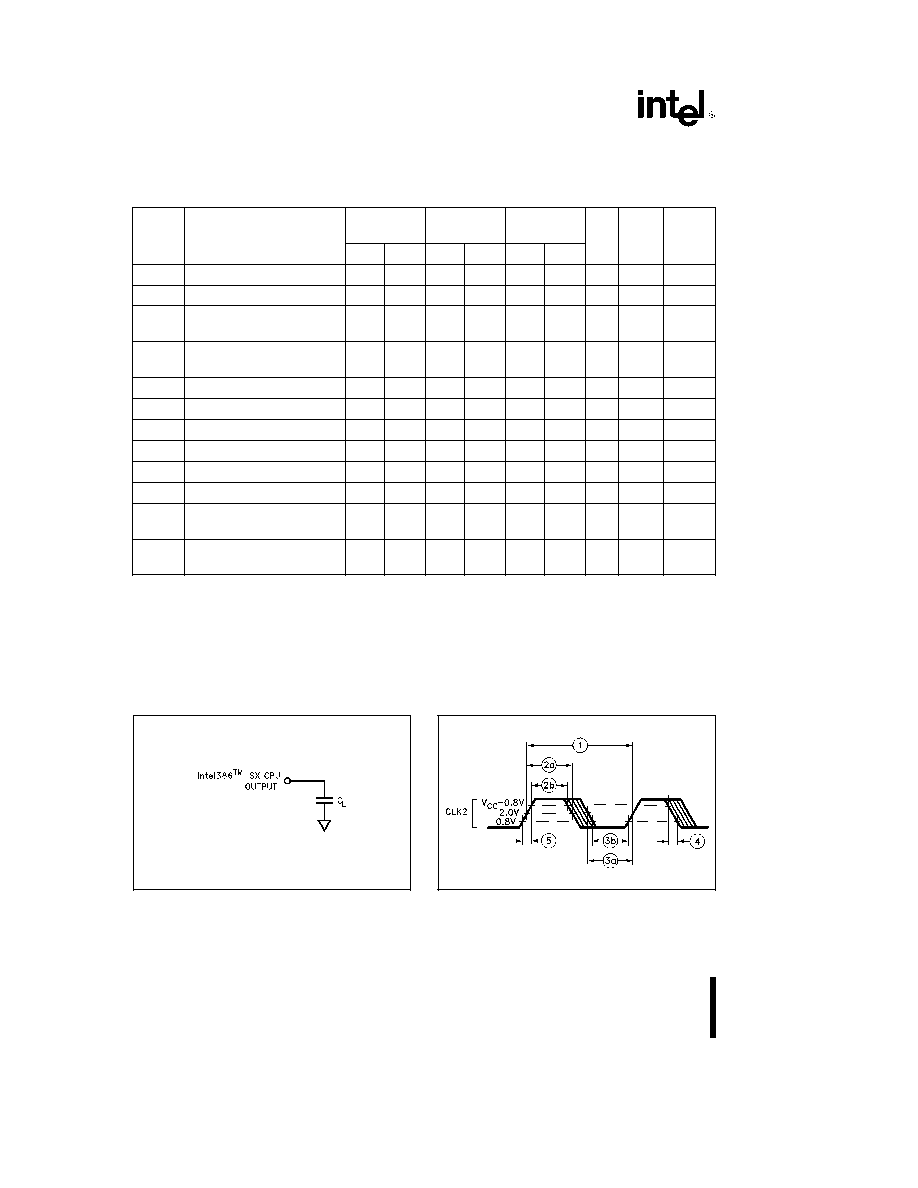
Intel386
TM
SX MICROPROCESSOR
Functional operating range V
CC
e
5V
g
10% T
CASE
e
0 C to 100 C
Table 7 8 Low Power (LP) Intel386
TM
SX
A C Characteristics
20 MHz 16 MHz and 12 MHz
(Continued)
Symbol
Parameter
20 MHz
16 MHz
12 MHz
Unit Figure
Notes
Intel386 SX
Intel386 SX
Intel386 SX
Min
Max
Min
Max
Min
Max
t
19
READY
Setup Time
12
19
19
ns
7 4
t
20
READY
Hold Time
4
4
4
ns
7 4
t
21
D15 � D0 Read Data
9
9
9
ns
7 4
Setup Time
t
22
D15 � D0 Read Data
6
6
6
ns
7 4
Hold Time
t
23
HOLD Setup Time
17
26
26
ns
7 4
t
24
HOLD Hold Time
5
5
7
ns
7 4
t
25
RESET Setup Time
12
13
15
ns
7 7
t
26
RESET Hold Time
4
4
6
ns
7 7
t
27
NMI INTR Setup Time
16
16
16
ns
7 4
(Note 2)
t
28
NMI INTR Hold Time
16
16
16
ns
7 4
(Note 2)
t
29
PEREQ ERROR
BUSY
14
16
16
ns
7 4
(Note 2)
FLT
Setup Time
t
30
PEREQ ERROR
BUSY
5
5
5
ns
7 4
(Note 2)
FLT
Hold Time
NOTES
1 Float condition occurs when maximum output current becomes less than I
LO
in magnitude Float delay is not 100%
tested
2 These inputs are allowed to be asynchronous to CLK2 The setup and hold specifications are given for testing purposes
to assure recognition within a specific CLK2 period
3 These are not tested They are guaranteed by design characterization
4 Tested with C
L
set at 50 pf and derated to support the indicated distributed capacitive load See Figures 7 8 though 7 10
for the capacitive derating curve
A C TEST LOADS
240187 � 36
A C TIMING WAVEFORMS
240187 � 37
Figure 7 2 A C Test Loads
Figure 7 3 CLK2 Waveform
74

Intel386
TM
SX MICROPROCESSOR
240187 � 38
Figure 7 4 A C Timing Waveforms
Input Setup and Hold Timing
240187 � 39
Figure 7 5 A C Timing Waveforms
Output Valid Delay Timing
75
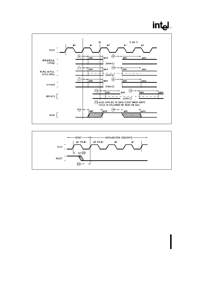
Intel386
TM
SX MICROPROCESSOR
240187 � 40
Figure 7 6 A C Timing Waveforms
Output Float Delay and HLDA Valid Delay Timing
240187 � 41
Figure 7 7 A C Timing Waveforms
RESET Setup and Hold Timing and Internal Phase
76

Intel386
TM
SX MICROPROCESSOR
240187 � 42
Figure 7 8 Typical Output Valid Delay versus
Load Capacitance at Maximum Operating
Temperature (C
L
e
120 pF)
240187 � 43
Figure 7 9 Typical Output Valid Delay versus
Load Capacitance at Maximum Operating
Temperature (C
L
e
75 pF)
240187 � 50
Figure 7 10 Typical Output Rise Time versus
Load Capacitance at Maximum Operating
Temperature
240187 � 45
Figure 7 11 Typical I
CC
vs Frequency
77
Intel386
TM
SX MICROPROCESSOR
240187 � 48
Figure 7 12 Preliminary ICE
TM
-Intel386
TM
SX Emulator User Cable with PQFP Adapter
240187 � 49
Figure 7 13 Preliminary ICE
TM
-Intel386
TM
SX Emulator User Cable with OIB and PQFP Adapter
7 5 Designing for the
ICE
TM
-Intel386
TM
SX Emulator
ICE-Intel386 SX is the in-circuit emulator for the In-
tel386
TM
SX CPU The ICE-386 SX emulator pro-
vides a 100-pin fine pitch flat-pack probe for connec-
tion to a socket located on the target system
Sockets that accept this probe are available from
3M (part
2-0100-07243-000) or from AMP (part
821959-1 and part
821949-4) The ICE-386 SX
emulator probe attaches to the target system via an
adapter that replaces the Intel386 SX component in
the target system
78

Intel386
TM
SX MICROPROCESSOR
Due to the high operating frequency of Intel386 SX
CPU based systems there is no buffering between
the Intel386 SX emulation processor (on the emula-
tor probe) and the target system A direct result of
the non-buffered interconnect is that the ICE-
Intel386 SX emulator shares the address and data
busses with the target system
In order to avoid problems with the shared bus and
maintain signal integrity the system designer must
adhere to the following guidelines
1 The bus controller must only enable data trans-
ceivers onto the data bus during valid read cycles
(initiated by assertion of ADS ) of the Intel386
SX CPU other local devices or other bus mas-
ters
2 Before another bus master drives the local proc-
essor address bus the other master must gain
control of the address bus by asserting HOLD
and receiving the HLDA response
3 The emulation processor receives the RESET
signal 2 or 4 CLK2 cycles later than an Intel386
SX CPU would and responds to RESET later
Correct phase of the response is guaranteed
In order to avoid problems that might arise due to
the shared busses an Optional use Isolation Board
(OIB) is included with the emulator hardware The
OIB may be used to provide buffering between the
emulation processor and the target system but in-
serts a delay of approximately 10 ns in signal path
In
addition
to
the
above
considerations
the
ICE-386 SX emulator processor module has several
electrical and mechanical characteristics that should
be taken into consideration when designing the
Intel386 SX CPU system
Capacitive Loading
ICE-Intel386 SX adds up to 27
pF to each Intel386 SX CPU signal
Drive Requirements
ICE-Intel386 SX adds one
FAST TTL load on the CLK2 control address and
data lines These loads are within the processor
module and are driven by the Intel386 SX CPU emu-
lation processor which has standard drive and load-
ing capability listed in Tables 7 3 and 7 4
Power Requirements
For noise immunity and
CMOS latch-up protection the ICE-Intel386 SX emu-
lator processor module is powered by the user sys-
tem
The circuitry on the processor module draws up to
1 4A including the maximum Intel386 SX CPU I
CC
from the user Intel386 SX CPU socket
Intel386 SX CPU Location and Orientation
The
ICE-Intel386 SX emulator processor module may re-
quire lateral clearance Figure 7 12 shows the clear-
ance requirements of the iMP adapter The optional
isolation board (OIB) which provides extra electrical
buffering and has the same lateral clearance re-
quirements as Figure 7 12 adds an additional 0 5
inches to the vertical clearance requirement This is
illustrated in Figure 7 13
Optional Isolation Board (OIB) and the CLK2
speed reduction
Due to the unbuffered probe de-
sign the ICE-Intel386 SX emulator is susceptible to
errors on the user's bus The OIB allows the ICE-
Intel386 SX emulator to function in user systems
with faults (shorted signals etc ) After electrical ver-
ification the OIB may be removed When the OIB is
installed the user system must have a maximum
CLK2 frequency of 20 MHz
8 0 DIFFERENCES BETWEEN THE
Intel386
TM
SX CPU AND THE
Intel386
TM
DX CPU
The following are the major differences between the
Intel386 SX CPU and the Intel386 DX CPU
1 The Intel386 SX CPU generates byte selects on
BHE
and BLE
(like the 8086 and 80286) to
distinguish the upper and lower bytes on its 16-bit
data bus The Intel386 DX CPU uses four byte
selects BE0 -BE3
to distinguish between the
different bytes on its 32-bit bus
2 The Intel386 SX CPU has no bus sizing option
The Intel386 DX CPU can select between either
a 32-bit bus or a 16-bit bus by use of the BS16
input The Intel386 SX CPU has a 16-bit bus size
3 The NA
pin operation in the Intel386 SX CPU is
identical to that of the NA
pin on the Intel386
DX CPU with one exception the Intel386 DX CPU
NA
pin cannot be activated on 16-bit bus cy-
cles (where BS16
is LOW in the Intel386 DX
CPU case) whereas NA
can be activated on
any Intel386 SX CPU bus cycle
4 The contents of all Intel386 SX CPU registers at
reset are identical to the contents of the Intel386
DX CPU registers at reset except the DX regis-
ter The DX register contains a component-step-
ping identifier at reset i e
in Intel386 DX CPU DH e 3 indicates Intel386
DX CPU after reset
DL e revision number
in Intel386 SX CPU
DH e 23H indicates
Intel386 SX CPU after reset
DL e revision number
79

Intel386
TM
SX MICROPROCESSOR
5 The Intel386 DX CPU uses A
31
and M IO
as
selects
for
the
numerics
coprocessor
The
Intel386 SX CPU uses A
23
and M IO
as selects
6 The Intel386 DX CPU prefetch unit fetches code
in four-byte units The Intel386 SX CPU prefetch
unit reads two bytes as one unit (like the 80286)
In BS16 mode the Intel386 DX CPU takes two
consecutive bus cycles to complete a prefetch re-
quest If there is a data read or write request after
the prefetch starts the Intel386 DX CPU will fetch
all four bytes before addressing the new request
7 Both Intel386 DX CPU and Intel386 SX CPU have
the same logical address space The only differ-
ence is that the Intel386 DX CPU has a 32-bit
physical address space and the Intel386 SX CPU
has a 24-bit physical address space The Intel386
SX CPU has a physical memory address space of
up to 16 megabytes instead of the 4 gigabytes
available to the Intel386 DX CPU Therefore in
Intel386 SX CPU systems the operating system
must be aware of this physical memory limit and
should allocate memory for applications programs
within this limit If a Intel386 DX CPU system uses
only the lower 16 megabytes of physical address
then there will be no extra effort required to mi-
grate Intel386 DX CPU software to the Intel386
SX CPU Any application which uses more than
16 megabytes of memory can run on the Intel386
SX CPU if the operating system utilizes the
Intel386 SX CPU's paging mechanism In spite of
this difference in physical address space the
Intel386 SX CPU and Intel386 DX CPU can run
the same operating systems and applications
within their respective physical memory con-
straints
8 The Intel386 SX has an input called FLT
which
tri-states all bidirectional and output pins includ-
ing HLDA
when asserted It is used with ON
Circuit Emulation (ONCE) In the Intel386 DX
CPU FLT
is found only on the plastic quad flat
package version and not on the ceramic pin grid
array version For a more detailed explanation of
FLT
and testability please refer to section 5 4
9 0 INSTRUCTION SET
This section describes the instruction set Table 9 1
lists all instructions along with instruction encoding
diagrams and clock counts Further details of the
instruction encoding are then provided in the follow-
ing sections which completely describe the encod-
ing structure and the definition of all fields occurring
within instructions
9 1 Intel386
TM
SX CPU Instruction
Encoding and Clock Count
Summary
To calculate elapsed time for an instruction multiply
the instruction clock count as listed in Table 9 1 be-
low by the processor clock period (e g 62 5 ns
for an Intel386 SX Microprocessor operating at
16 MHz) The actual clock count of an Intel386 SX
Microprocessor program will average 5% more than
the calculated clock count due to instruction se-
quences which execute faster than they can be
fetched from memory
Instruction Clock Count Assumptions
1 The instruction has been prefetched decoded
and is ready for execution
2 Bus cycles do not require wait states
3 There are no local bus HOLD requests delaying
processor access to the bus
4 No exceptions are detected during instruction ex-
ecution
5 If an effective address is calculated it does not
use two general register components One regis-
ter scaling and displacement can be used within
the clock counts shown However if the effective
address calculation uses two general register
components add 1 clock to the clock count
shown
Instruction Clock Count Notation
1 If two clock counts are given the smaller refers to
a register operand and the larger refers to a mem-
ory operand
2 n e number of times repeated
3 m e number of components in the next instruc-
tion executed where the entire displacement (if
any) counts as one component the entire imme-
diate data (if any) counts as one component and
all other bytes of the instruction and prefix(es)
each count as one component
Misaligned or 32-Bit Operand Accesses
If instructions accesses a misaligned 16-bit oper-
and or 32-bit operand on even address add
2
clocks for read or write
4
clocks for read and write
If instructions accesses a 32-bit operand on odd
address add
4
clocks for read or write
8
clocks for read and write
Wait States
Wait states add 1 clock per wait state to instruction
execution for each data access
80
Intel386
TM
SX MICROPROCESSOR
Table 9-1 Instruction Set Clock Count Summary
CLOCK COUNT
NOTES
Real
Real
INSTRUCTION
FORMAT
Address
Protected
Address
Protected
Mode or
Virtual
Mode or
Virtual
Virtual
Address
Virtual
Address
8086
Mode
8086
Mode
Mode
Mode
GENERAL DATA TRANSFER
MOV
e
Move
Register to Register Memory
1 0 0 0 1 0 0 w
mod reg
r m
2 2
2 2
b
h
Register Memory to Register
1 0 0 0 1 0 1 w
mod reg
r m
2 4
2 4
b
h
Immediate to Register Memory
1 1 0 0 0 1 1 w
mod 0 0 0
r m
immediate data
2 2
2 2
b
h
Immediate to Register (short form)
1 0 1 1 w
reg
immediate data
2
2
Memory to Accumulator (short form)
1 0 1 0 0 0 0 w
full displacement
4
4
b
h
Accumulator to Memory (short form)
1 0 1 0 0 0 1 w
full displacement
2
2
b
h
Register Memory to Segment Register
1 0 0 0 1 1 1 0
mod sreg3 r m
2 5
22 23
b
h i j
Segment Register to Register Memory
1 0 0 0 1 1 0 0
mod sreg3 r m
2 2
2 2
b
h
MOVSX
e
Move With Sign Extension
Register From Register Memory
0 0 0 0 1 1 1 1
1 0 1 1 1 1 1 w
mod reg
r m
3 6
3 6
b
h
MOVZX
e
Move With Zero Extension
Register From Register Memory
0 0 0 0 1 1 1 1
1 0 1 1 0 1 1 w
mod reg
r m
3 6
3 6
b
h
PUSH
e
Push
Register Memory
1 1 1 1 1 1 1 1
mod 1 1 0
r m
5 7
7 9
b
h
Register (short form)
0 1 0 1 0
reg
2
4
b
h
(short form)
Segment Register (ES CS SS or DS)
0 0 0 sreg2 1 1 0
2
4
b
h
FS or GS)
Segment Register (ES CS SS DS
0 0 0 0 1 1 1 1
1 0 sreg3 0 0 0
2
4
b
h
Immediate
0 1 1 0 1 0 s 0
immediate data
2
4
b
h
PUSHA
e
Push All
0 1 1 0 0 0 0 0
18
34
b
h
POP
e
Pop
Register Memory
1 0 0 0 1 1 1 1
mod 0 0 0
r m
5 7
7 9
b
h
Register (short form)
0 1 0 1 1
reg
6
6
b
h
(short form)
Segment Register (ES CS SS or DS)
0 0 0 sreg 2 1 1 1
7
25
b
h i j
FS or GS
Segment Register (ES CS SS or DS)
0 0 0 0 1 1 1 1
1 0 sreg 3 0 0 1
7
25
b
h i j
POPA
e
Pop All
0 1 1 0 0 0 0 1
24
40
b
h
XCHG
e
Exchange
Register Memory With Register
1 0 0 0 0 1 1 w
mod reg
r m
3 5
3 5
b f
f h
Register With Accumulator (short form)
1 0 0 1 0
reg
8086 Mode
Clk Count
Virtual
3
3
IN
e
Input from
Fixed Port
1 1 1 0 0 1 0 w
port number
26
12
6
26
s t m
Variable Port
1 1 1 0 1 1 0 w
27
13
7
27
s t m
OUT
e
Output to
Fixed Port
1 1 1 0 0 1 1 w
port number
24
10
4
24
s t m
Variable Port
1 1 1 0 1 1 1 w
25
11
5
25
s t m
LEA
e
Load EA to Register
1 0 0 0 1 1 0 1
mod reg
r m
2
2
81

Intel386
TM
SX MICROPROCESSOR
Table 9-1 Instruction Set Clock Count Summary
(Continued)
CLOCK COUNT
NOTES
Real
Real
INSTRUCTION
FORMAT
Address
Protected
Address
Protected
Mode or
Virtual
Mode or
Virtual
Virtual
Address
Virtual
Address
8086
Mode
8086
Mode
Mode
Mode
SEGMENT CONTROL
LDS
e
Load Pointer to DS
1 1 0 0 0 1 0 1
mod reg
r m
7
26
28
b
h i j
LES
e
Load Pointer to ES
1 1 0 0 0 1 0 0
mod reg
r m
7
26
28
b
h i j
LFS
e
Load Pointer to FS
0 0 0 0 1 1 1 1
1 0 1 1 0 1 0 0
mod reg
r m
7
29
31
b
h i j
LGS
e
Load Pointer to GS
0 0 0 0 1 1 1 1
1 0 1 1 0 1 0 1
mod reg
r m
7
26
28
b
h i j
LSS
e
Load Pointer to SS
0 0 0 0 1 1 1 1
1 0 1 1 0 0 1 0
mod reg
r m
7
26
28
b
h i j
FLAG CONTROL
CLC
e
Clear Carry Flag
1 1 1 1 1 0 0 0
2
2
CLD
e
Clear Direction Flag
1 1 1 1 1 1 0 0
2
2
CLI
e
Clear Interrupt Enable Flag
1 1 1 1 1 0 1 0
8
8
m
CLTS
e
Clear Task Switched Flag
0 0 0 0 1 1 1 1
0 0 0 0 0 1 1 0
5
5
c
l
CMC
e
Complement Carry Flag
1 1 1 1 0 1 0 1
2
2
LAHF
e
Load AH into Flag
1 0 0 1 1 1 1 1
2
2
POPF
e
Pop Flags
1 0 0 1 1 1 0 1
5
5
b
h n
PUSHF
e
Push Flags
1 0 0 1 1 1 0 0
4
4
b
h
SAHF
e
Store AH into Flags
1 0 0 1 1 1 1 0
3
3
STC
e
Set Carry Flag
1 1 1 1 1 0 0 1
2
2
STD
e
Set Direction Flag
1 1 1 1 1 1 0 1
STI
e
Set Interrupt Enable Flag
1 1 1 1 1 0 1 1
8
8
m
ARITHMETIC
ADD
e
Add
Register to Register
0 0 0 0 0 0 d w
mod reg
r m
2
2
Register to Memory
0 0 0 0 0 0 0 w
mod reg
r m
7
7
b
h
Memory to Register
0 0 0 0 0 0 1 w
mod reg
r m
6
6
b
h
Immediate to Register Memory
1 0 0 0 0 0 s w
mod 0 0 0
r m
immediate data
2 7
2 7
b
h
Immediate to Accumulator (short form)
0 0 0 0 0 1 0 w
immediate data
2
2
ADC
e
Add With Carry
Register to Register
0 0 0 1 0 0 d w
mod reg
r m
2
2
Register to Memory
0 0 0 1 0 0 0 w
mod reg
r m
7
7
b
h
Memory to Register
0 0 0 1 0 0 1 w
mod reg
r m
6
6
b
h
Immediate to Register Memory
1 0 0 0 0 0 s w
mod 0 1 0
r m
immediate data
2 7
2 7
b
h
Immediate to Accumulator (short form)
0 0 0 1 0 1 0 w
immediate data
2
2
INC
e
Increment
Register Memory
1 1 1 1 1 1 1 w
mod 0 0 0
r m
2 6
2 6
b
h
Register (short form)
0 1 0 0 0
reg
2
2
SUB
e
Subtract
Register from Register
0 0 1 0 1 0 d w
mod reg
r m
2
2
82

Intel386
TM
SX MICROPROCESSOR
Table 9-1 Instruction Set Clock Count Summary
(Continued)
CLOCK COUNT
NOTES
Real
Real
INSTRUCTION
FORMAT
Address
Protected
Address
Protected
Mode or
Virtual
Mode or
Virtual
Virtual
Address
Virtual
Address
8086
Mode
8086
Mode
Mode
Mode
ARITHMETIC
(Continued)
Register from Memory
0 0 1 0 1 0 0 w mod reg
r m
7
7
b
h
Memory from Register
0 0 1 0 1 0 1 w mod reg
r m
6
6
b
h
Immediate from Register Memory
1 0 0 0 0 0 s w mod 1 0 1
r m immediate data
2 7
2 7
b
h
Immediate from Accumulator (short form)
0 0 1 0 1 1 0 w
immediate data
2
2
SBB
e
Subtract with Borrow
Register from Register
0 0 0 1 1 0 d w mod reg
r m
2
2
Register from Memory
0 0 0 1 1 0 0 w mod reg
r m
7
7
b
h
Memory from Register
0 0 0 1 1 0 1 w mod reg
r m
6
6
b
h
Immediate from Register Memory
1 0 0 0 0 0 s w mod 0 1 1
r m immediate data
2 7
2 7
b
h
Immediate from Accumulator (short form)
0 0 0 1 1 1 0 w
immediate data
2
2
DEC
e
Decrement
Register Memory
1 1 1 1 1 1 1 w reg 0 0 1
r m
2 6
2 6
b
h
Register (short form)
0 1 0 0 1
reg
2
2
CMP
e
Compare
Register with Register
0 0 1 1 1 0 d w mod reg
r m
2
2
Memory with Register
0 0 1 1 1 0 0 w mod reg
r m
5
5
b
h
Register with Memory
0 0 1 1 1 0 1 w mod reg
r m
6
6
b
h
Immediate with Register Memory
1 0 0 0 0 0 s w mod 1 1 1
r m immediate data
2 5
2 5
b
h
Immediate with Accumulator (short form)
0 0 1 1 1 1 0 w
immediate data
2
2
NEG
e
Change Sign
1 1 1 1 0 1 1 w mod 0 1 1
r m
2 6
2 6
b
h
AAA
e
ASCII Adjust for Add
0 0 1 1 0 1 1 1
4
4
AAS
e
ASCII Adjust for Subtract
0 0 1 1 1 1 1 1
4
4
DAA
e
Decimal Adjust for Add
0 0 1 0 0 1 1 1
4
4
DAS
e
Decimal Adjust for Subtract
0 0 1 0 1 1 1 1
4
4
MUL
e
Multiply (unsigned)
Accumulator with Register Memory
1 1 1 1 0 1 1 w mod 1 0 0
r m
Multiplier-Byte
12�17 15�20
12�17 15�20
b d
d h
-Word
12�25 15�28
12�25 15�28
b d
d h
-Doubleword
12�41 17�46
12�41 17�46
b d
d h
IMUL
e
Integer Multiply (signed)
Accumulator with Register Memory
1 1 1 1 0 1 1 w mod 1 0 1
r m
Multiplier-Byte
12�17 15�20
12�17 15�20
b d
d h
-Word
12�25 15�28
12�25 15�28
b d
d h
-Doubleword
12�41 17�46
12�41 17�46
b d
d h
Register with Register Memory
0 0 0 0 1 1 1 1
1 0 1 0 1 1 1 1 mod reg
r m
Multiplier-Byte
12�17 15�20
12�17 15�20
b d
d h
-Word
12�25 15�28
12�25 15�28
b d
d h
-Doubleword
12�41 17�46
12�41 17�46
b d
d h
Register Memory with Immediate to Register 0 1 1 0 1 0 s 1 mod reg
r m immediate data
-Word
13�26
13�26 14�27
b d
d h
-Doubleword
13�42
13�42 16�45
b d
d h
83

Intel386
TM
SX MICROPROCESSOR
Table 9-1 Instruction Set Clock Count Summary
(Continued)
CLOCK COUNT
NOTES
Real
Real
INSTRUCTION
FORMAT
Address Protected Address Protected
Mode or
Virtual
Mode or
Virtual
Virtual
Address
Virtual
Address
8086
Mode
8086
Mode
Mode
Mode
ARITHMETIC
(Continued)
DIV
e
Divide (Unsigned)
Accumulator by Register Memory
1 1 1 1 0 1 1 w mod 1 1 0
r m
Divisor
Byte
14 17
14 17
b e
e h
Word
22 25
22 25
b e
e h
Doubleword
38 43
38 43
b e
e h
IDIV
e
Integer Divide (Signed)
Accumulator By Register Memory
1 1 1 1 0 1 1 w mod 1 1 1
r m
Divisor
Byte
19 22
19 22
b e
e h
Word
27 30
27 30
b e
e h
Doubleword
43 48
43 48
b e
e h
AAD
e
ASCII Adjust for Divide
1 1 0 1 0 1 0 1
0 0 0 0 1 0 1 0
19
19
AAM
e
ASCII Adjust for Multiply
1 1 0 1 0 1 0 0
0 0 0 0 1 0 1 0
17
17
CBW
e
Convert Byte to Word
1 0 0 1 1 0 0 0
3
3
CWD
e
Convert Word to Double Word
1 0 0 1 1 0 0 1
2
2
LOGIC
Shift Rotate Instructions
Not Through Carry (ROL ROR SAL SAR SHL and SHR)
Register Memory by 1
1 1 0 1 0 0 0 w mod TTT
r m
3 7
3 7
b
h
Register Memory by CL
1 1 0 1 0 0 1 w mod TTT
r m
3 7
3 7
b
h
Register Memory by Immediate Count
1 1 0 0 0 0 0 w mod TTT
r m immed 8-bit data
3 7
3 7
b
h
Through Carry (RCL and RCR)
Register Memory by 1
1 1 0 1 0 0 0 w mod TTT
r m
9 10
9 10
b
h
Register Memory by CL
1 1 0 1 0 0 1 w mod TTT
r m
9 10
9 10
b
h
Register Memory by Immediate Count
1 1 0 0 0 0 0 w mod TTT
r m immed 8-bit data
9 10
9 10
b
h
T T T Instruction
0 0 0
ROL
0 0 1
ROR
0 1 0
RCL
0 1 1
RCR
1 0 0
SHL SAL
1 0 1
SHR
1 1 1
SAR
SHLD
e
Shift Left Double
Register Memory by Immediate
0 0 0 0 1 1 1 1
1 0 1 0 0 1 0 0 mod reg
r m immed 8-bit data
3 7
3 7
Register Memory by CL
0 0 0 0 1 1 1 1
1 0 1 0 0 1 0 1 mod reg
r m
3 7
3 7
SHRD
e
Shift Right Double
Register Memory by Immediate
0 0 0 0 1 1 1 1
1 0 1 0 1 1 0 0 mod reg
r m immed 8-bit data
3 7
3 7
Register Memory by CL
0 0 0 0 1 1 1 1
1 0 1 0 1 1 0 1 mod reg
r m
3 7
3 7
AND
e
And
Register to Register
0 0 1 0 0 0 d w mod reg
r m
2
2
84

Intel386
TM
SX MICROPROCESSOR
Table 9-1 Instruction Set Clock Count Summary
(Continued)
CLOCK COUNT
NOTES
Real
Real
INSTRUCTION
FORMAT
Address
Protected
Address
Protected
Mode or
Virtual
Mode or
Virtual
Virtual
Address
Virtual
Address
8086
Mode
8086
Mode
Mode
Mode
LOGIC
(Continued)
Register to Memory
0 0 1 0 0 0 0 w
mod reg
r m
7
7
b
h
Memory to Register
0 0 1 0 0 0 1 w
mod reg
r m
6
6
b
h
Immediate to Register Memory
1 0 0 0 0 0 0 w
mod 1 0 0
r m immediate data
2 7
2 7
b
h
Immediate to Accumulator (Short Form)
0 0 1 0 0 1 0 w
immediate data
2
2
TEST
e
And Function to Flags No Result
Register Memory and Register
1 0 0 0 0 1 0 w
mod reg
r m
2 5
2 5
b
h
Immediate Data and Register Memory
1 1 1 1 0 1 1 w
mod 0 0 0
r m immediate data
2 5
2 5
b
h
Immediate Data and Accumulator
(Short Form)
1 0 1 0 1 0 0 w
immediate data
2
2
OR
e
Or
Register to Register
0 0 0 0 1 0 d w
mod reg
r m
2
2
Register to Memory
0 0 0 0 1 0 0 w
mod reg
r m
7
7
b
h
Memory to Register
0 0 0 0 1 0 1 w
mod reg
r m
6
6
b
h
Immediate to Register Memory
1 0 0 0 0 0 0 w
mod 0 0 1
r m immediate data
2 7
2 7
b
h
Immediate to Accumulator (Short Form)
0 0 0 0 1 1 0 w
immediate data
2
2
XOR
e
Exclusive Or
Register to Register
0 0 1 1 0 0 d w
mod reg
r m
2
2
Register to Memory
0 0 1 1 0 0 0 w
mod reg
r m
7
7
b
h
Memory to Register
0 0 1 1 0 0 1 w
mod reg
r m
6
6
b
h
Immediate to Register Memory
1 0 0 0 0 0 0 w
mod 1 1 0
r m immediate data
2 7
2 7
b
h
Immediate to Accumulator (Short Form)
0 0 1 1 0 1 0 w
immediate data
2
2
NOT
e
Invert Register Memory
1 1 1 1 0 1 1 w
mod 0 1 0
r m
2 6
2 6
b
h
STRING MANIPULATION
CMPS
e
Compare Byte Word
1 0 1 0 0 1 1 w
Virtual
Count
Mode
8086
Clk
10
10
b
h
INS
e
Input Byte Word from DX Port
0 1 1 0 1 1 0 w
29
15
9
29
b
s t h m
LODS
e
Load Byte Word to AL AX EAX
1 0 1 0 1 1 0 w
5
5
b
h
MOVS
e
Move Byte Word
1 0 1 0 0 1 0 w
7
7
b
h
OUTS
e
Output Byte Word to DX Port
0 1 1 0 1 1 1 w
28
14
8
28
b
s t h m
SCAS
e
Scan Byte Word
1 0 1 0 1 1 1 w
7
7
b
h
STOS
e
Store Byte Word from
AL AX EX
1 0 1 0 1 0 1 w
4
4
b
h
XLAT
e
Translate String
1 1 0 1 0 1 1 1
5
5
h
REPEATED STRING MANIPULATION
Repeated by Count in CX or ECX
REPE CMPS
e
Compare String
(Find Non-Match)
1 1 1 1 0 0 1 1
1 0 1 0 0 1 1 w
5
a
9n
5
a
9n
b
h
85
Intel386
TM
SX MICROPROCESSOR
Table 9-1 Instruction Set Clock Count Summary
(Continued)
CLOCK COUNT
NOTES
Real
Real
INSTRUCTION
FORMAT
Address
Protected Address
Protected
Mode or
Virtual
Mode or
Virtual
Virtual
Address
Virtual
Address
8086
Mode
8086
Mode
Mode
Mode
REPEATED STRING MANIPULATION
(Continued)
REPNE CMPS
e
Compare String
(Find Match)
1 1 1 1 0 0 1 0
1 0 1 0 0 1 1 w
8086 Mode
Clk Count
Virtual
5
a
9n
5
a
9n
b
h
REP INS
e
Input String
1 1 1 1 0 0 1 0
0 1 1 0 1 1 0 w
13
a
6n
7
a
6n
b
s t h m
27
a
6n
REP LODS
e
Load String
1 1 1 1 0 0 1 0
1 0 1 0 1 1 0 w
5
a
6n
5
a
6n
b
h
REP MOVS
e
Move String
1 1 1 1 0 0 1 0
1 0 1 0 0 1 0 w
7
a
4n
7
a
4n
b
h
REP OUTS
e
Output String
1 1 1 1 0 0 1 0
0 1 1 0 1 1 1 w
12
a
5n
6
a
5n
b
s t h m
26
a
5n
REPE SCAS
e
Scan String
(Find Non-AL AX EAX)
1 1 1 1 0 0 1 1
1 0 1 0 1 1 1 w
5
a
8n
5
a
8n
b
h
REPNE SCAS
e
Scan String
(Find AL AX EAX)
1 1 1 1 0 0 1 0
1 0 1 0 1 1 1 w
5
a
8n
5
a
8n
b
h
REP STOS
e
Store String
1 1 1 1 0 0 1 0
1 0 1 0 1 0 1 w
5
a
5n
5
a
5n
b
h
BIT MANIPULATION
BSF
e
Scan Bit Forward
0 0 0 0 1 1 1 1
1 0 1 1 1 1 0 0 mod reg
r m
10
a
3n
10
a
3n
b
h
BSR
e
Scan Bit Reverse
0 0 0 0 1 1 1 1
1 0 1 1 1 1 0 1 mod reg
r m
10
a
3n
10
a
3n
b
h
BT
e
Test Bit
Register Memory Immediate
0 0 0 0 1 1 1 1
1 0 1 1 1 0 1 0 mod 1 0 0
r m immed 8-bit data
3 6
3 6
b
h
Register Memory Register
0 0 0 0 1 1 1 1
1 0 1 0 0 0 1 1 mod reg
r m
3 12
3 12
b
h
BTC
e
Test Bit and Complement
Register Memory Immediate
0 0 0 0 1 1 1 1
1 0 1 1 1 0 1 0 mod 1 1 1
r m immed 8-bit data
6 8
6 8
b
h
Register Memory Register
0 0 0 0 1 1 1 1
1 0 1 1 1 0 1 1 mod reg
r m
6 13
6 13
b
h
BTR
e
Test Bit and Reset
Register Memory Immediate
0 0 0 0 1 1 1 1
1 0 1 1 1 0 1 0 mod 1 1 0
r m immed 8-bit data
6 8
6 8
b
h
Register Memory Register
0 0 0 0 1 1 1 1
1 0 1 1 0 0 1 1 mod reg
r m
6 13
6 13
b
h
BTS
e
Test Bit and Set
Register Memory Immediate
0 0 0 0 1 1 1 1
1 0 1 1 1 0 1 0 mod 1 0 1
r m immed 8-bit data
6 8
6 8
b
h
Register Memory Register
0 0 0 0 1 1 1 1
1 0 1 0 1 0 1 1 mod reg
r m
6 13
6 13
b
h
CONTROL TRANSFER
CALL
e
Call
Direct Within Segment
1 1 1 0 1 0 0 0
full displacement
7
a
m
9
a
m
b
r
Register Memory
Indirect Within Segment
1 1 1 1 1 1 1 1 mod 0 1 0
r m
7
a
m
10
a
m
9
a
m
b
h r
12
a
m
Direct Intersegment
1 0 0 1 1 0 1 0 unsigned full offset selector
17
a
m
42
a
m
b
j k r
NOTE
Clock count shown applies if I O permission allows I O to the port in virtual 8086 mode If I O bit map denies permission
exception 13 fault occurs refer to clock counts for INT 3 instruction
86

Intel386
TM
SX MICROPROCESSOR
Table 9-1 Instruction Set Clock Count Summary
(Continued)
CLOCK COUNT
NOTES
Real
Real
INSTRUCTION
FORMAT
Address
Protected
Address
Protected
Mode or
Virtual
Mode or
Virtual
Virtual
Address
Virtual
Address
8086
Mode
8086
Mode
Mode
Mode
CONTROL TRANSFER
(Continued)
Protected Mode Only (Direct Intersegment)
Via Call Gate to Same Privilege Level
64
a
m
h j k r
Via Call Gate to Different Privilege Level
(No Parameters)
98
a
m
h j k r
Via Call Gate to Different Privilege Level
(x Parameters)
106
a
8x
a
m
h j k r
From 286 Task to 286 TSS
285
h j k r
From 286 Task to Intel386
TM
SX CPU TSS
310
h j k r
From 286 Task to Virtual 8086 Task (Intel386 SX CPU TSS)
229
h j k r
From Intel386 SX CPU Task to 286 TSS
285
h j k r
From Intel386 SX CPU Task to Intel386 SX CPU TSS
392
h j k r
From Intel386 SX CPU Task to Virtual 8086 Task (Intel386 SX CPU TSS)
309
h j k r
Indirect Intersegment
1 1 1 1 1 1 1 1 mod 0 1 1
r m
30
a
m
46
a
m
b
h j k r
Protected Mode Only (Indirect Intersegment)
Via Call Gate to Same Privilege Level
68
a
m
h j k r
Via Call Gate to Different Privilege Level
(No Parameters)
102
a
m
h j k r
Via Call Gate to Different Privilege Level
(x Parameters)
110
a
8x
a
m
h j k r
From 286 Task to 286 TSS
h j k r
From 286 Task to Intel386 SX CPU TSS
h j k r
From 286 Task to Virtual 8086 Task (Intel386 SX CPU TSS)
h j k r
From Intel386 SX CPU Task to 286 TSS
h j k r
From Intel386 SX CPU Task to Intel386 SX CPU TSS
399
h j k r
From Intel386 SX CPU Task to Virtual 8086 Task (Intel386 SX CPU TSS)
h j k r
JMP
e
Unconditional Jump
Short
1 1 1 0 1 0 1 1 8-bit displacement
7
a
m
7
a
m
r
Direct within Segment
1 1 1 0 1 0 0 1
full displacement
7
a
m
7
a
m
r
within Segment
Register Memory Indirect
1 1 1 1 1 1 1 1 mod 1 0 0
r m
9
a
m 14
a
m 9
a
m 14
a
m
b
h r
Direct Intersegment
1 1 1 0 1 0 1 0 unsigned full offset selector
16
a
m
31
a
m
j k r
Protected Mode Only (Direct Intersegment)
Via Call Gate to Same Privilege Level
53
a
m
h j k r
From 286 Task to 286 TSS
h j k r
From 286 Task to Intel386 SX CPU TSS
h j k r
From 286 Task to Virtual 8086 Task (Intel386 SX CPU TSS)
h j k r
From Intel386 SX CPU Task to 286 TSS
h j k r
From Intel386 SX CPU Task to Intel386 SX CPU TSS
h j k r
From Intel386 SX CPU Task to Virtual 8086 Task (Intel386 SX CPU TSS)
395
h j k r
Indirect Intersegment
1 1 1 1 1 1 1 1 mod 1 0 1
r m
17
a
m
31
a
m
b
h j k r
Protected Mode Only (Indirect Intersegment)
Via Call Gate to Same Privilege Level
49
a
m
h j k r
From 286 Task to 286 TSS
h j k r
From 286 Task to Intel386 SX CPU TSS
h j k r
From 286 Task to Virtual 8086 Task (Intel386 SX CPU TSS)
h j k r
From Intel386 SX CPU Task to 286 TSS
h j k r
From Intel386 SX CPU Task to Intel386 SX CPU TSS
328
h j k r
From Intel386 SX CPU Task to Virtual 8086 Task (Intel386 SX CPU TSS)
h j k r
87

Intel386
TM
SX MICROPROCESSOR
Table 9-1 Instruction Set Clock Count Summary
(Continued)
CLOCK COUNT
NOTES
Real
Real
INSTRUCTION
FORMAT
Address
Protected
Address
Protected
Mode or
Virtual
Mode or
Virtual
Virtual
Address
Virtual
Address
8086
Mode
8086
Mode
Mode
Mode
CONTROL TRANSFER
(Continued)
RET
e
Return from CALL
Within Segment
1 1 0 0 0 0 1 1
12
a
m
b
g h r
Within Segment Adding Immediate to SP
1 1 0 0 0 0 1 0
16-bit displ
12
a
m
b
g h r
Intersegment
1 1 0 0 1 0 1 1
36
a
m
b
g h j k r
Intersegment Adding Immediate to SP
1 1 0 0 1 0 1 0
16-bit displ
36
a
m
b
g h j k r
Protected Mode Only (RET)
to Different Privilege Level
Intersegment
72
h j k r
Intersegment Adding Immediate to SP
72
h j k r
CONDITIONAL JUMPS
NOTE Times Are Jump ``Taken or Not Taken''
JO
e
Jump on Overflow
8-Bit Displacement
0 1 1 1 0 0 0 0
8-bit displ
7
a
m or 3
7
a
m or 3
r
Full Displacement
0 0 0 0 1 1 1 1
1 0 0 0 0 0 0 0
full displacement
7
a
m or 3
7
a
m or 3
r
JNO
e
Jump on Not Overflow
8-Bit Displacement
0 1 1 1 0 0 0 1
8-bit displ
7
a
m or 3
7
a
m or 3
r
Full Displacement
0 0 0 0 1 1 1 1
1 0 0 0 0 0 0 1
full displacement
7
a
m or 3
7
a
m or 3
r
JB JNAE
e
Jump on Below Not Above or Equal
8-Bit Displacement
0 1 1 1 0 0 1 0
8-bit displ
7
a
m or 3
7
a
m or 3
r
Full Displacement
0 0 0 0 1 1 1 1
1 0 0 0 0 0 1 0
full displacement
7
a
m or 3
7
a
m or 3
r
JNB JAE
e
Jump on Not Below Above or Equal
8-Bit Displacement
0 1 1 1 0 0 1 1
8-bit displ
7
a
m or 3
7
a
m or 3
r
Full Displacement
0 0 0 0 1 1 1 1
1 0 0 0 0 0 1 1
full displacement
7
a
m or 3
7
a
m or 3
r
JE JZ
e
Jump on Equal Zero
8-Bit Displacement
0 1 1 1 0 1 0 0
8-bit displ
7
a
m or 3
7
a
m or 3
r
Full Displacement
0 0 0 0 1 1 1 1
1 0 0 0 0 1 0 0
full displacement
7
a
m or 3
7
a
m or 3
r
JNE JNZ
e
Jump on Not Equal Not Zero
8-Bit Displacement
0 1 1 1 0 1 0 1
8-bit displ
7
a
m or 3
7
a
m or 3
r
Full Displacement
0 0 0 0 1 1 1 1
1 0 0 0 0 1 0 1
full displacement
7
a
m or 3
7
a
m or 3
r
JBE JNA
e
Jump on Below or Equal Not Above
8-Bit Displacement
0 1 1 1 0 1 1 0
8-bit displ
7
a
m or 3
7
a
m or 3
r
Full Displacement
0 0 0 0 1 1 1 1
1 0 0 0 0 1 1 0
full displacement
7
a
m or 3
7
a
m or 3
r
JNBE JA
e
Jump on Not Below or Equal Above
8-Bit Displacement
0 1 1 1 0 1 1 1
8-bit displ
7
a
m or 3
7
a
m or 3
r
Full Displacement
0 0 0 0 1 1 1 1
1 0 0 0 0 1 1 1
full displacement
7
a
m or 3
7
a
m or 3
r
JS
e
Jump on Sign
8-Bit Displacement
0 1 1 1 1 0 0 0
8-bit displ
7
a
m or 3
7
a
m or 3
r
Full Displacement
0 0 0 0 1 1 1 1
1 0 0 0 1 0 0 0
full displacement
7
a
m or 3
7
a
m or 3
r
88
Intel386
TM
SX MICROPROCESSOR
Table 9-1 Instruction Set Clock Count Summary
(Continued)
CLOCK COUNT
NOTES
Real
Real
INSTRUCTION
FORMAT
Address
Protected
Address
Protected
Mode or
Virtual
Mode or
Virtual
Virtual
Address
Virtual
Address
8086
Mode
8086
Mode
Mode
Mode
CONDITIONAL JUMPS
(Continued)
JNS
e
Jump on Not Sign
8-Bit Displacement
0 1 1 1 1 0 0 1
8-bit displ
7
a
m or 3
7
a
m or 3
r
Full Displacement
0 0 0 0 1 1 1 1
1 0 0 0 1 0 0 1
full displacement
7
a
m or 3
7
a
m or 3
r
JP JPE
e
Jump on Parity Parity Even
8-Bit Displacement
0 1 1 1 1 0 1 0
8-bit displ
7
a
m or 3
7
a
m or 3
r
Full Displacement
0 0 0 0 1 1 1 1
1 0 0 0 1 0 1 0
full displacement
7
a
m or 3
7
a
m or 3
r
JNP JPO
e
Jump on Not Parity Parity Odd
8-Bit Displacement
0 1 1 1 1 0 1 1
8-bit displ
7
a
m or 3
7
a
m or 3
r
Full Displacement
0 0 0 0 1 1 1 1
1 0 0 0 1 0 1 1
full displacement
7
a
m or 3
7
a
m or 3
r
JL JNGE
e
Jump on Less Not Greater or Equal
8-Bit Displacement
0 1 1 1 1 1 0 0
8-bit displ
7
a
m or 3
7
a
m or 3
r
Full Displacement
0 0 0 0 1 1 1 1
1 0 0 0 1 1 0 0
full displacement
7
a
m or 3
7
a
m or 3
r
JNL JGE
e
Jump on Not Less Greater or Equal
8-Bit Displacement
0 1 1 1 1 1 0 1
8-bit displ
7
a
m or 3
7
a
m or 3
r
Full Displacement
0 0 0 0 1 1 1 1
1 0 0 0 1 1 0 1
full displacement
7
a
m or 3
7
a
m or 3
r
JLE JNG
e
Jump on Less or Equal Not Greater
8-Bit Displacement
0 1 1 1 1 1 1 0
8-bit displ
7
a
m or 3
7
a
m or 3
r
Full Displacement
0 0 0 0 1 1 1 1
1 0 0 0 1 1 1 0
full displacement
7
a
m or 3
7
a
m or 3
r
JNLE JG
e
Jump on Not Less or Equal Greater
8-Bit Displacement
0 1 1 1 1 1 1 1
8-bit displ
7
a
m or 3
7
a
m or 3
r
Full Displacement
0 0 0 0 1 1 1 1
1 0 0 0 1 1 1 1
full displacement
7
a
m or 3
7
a
m or 3
r
JCXZ
e
Jump on CX Zero
1 1 1 0 0 0 1 1
8-bit displ
9
a
m or 5
9
a
m or 5
r
JECXZ
e
Jump on ECX Zero
1 1 1 0 0 0 1 1
8-bit displ
9
a
m or 5
9
a
m or 5
r
(Address Size Prefix Differentiates JCXZ from JECXZ)
LOOP
e
Loop CX Times
1 1 1 0 0 0 1 0
8-bit displ
11
a
m
11
a
m
r
LOOPZ LOOPE
e
Loop with
Zero Equal
1 1 1 0 0 0 0 1
8-bit displ
11
a
m
11
a
m
r
LOOPNZ LOOPNE
e
Loop While
Not Zero
1 1 1 0 0 0 0 0
8-bit displ
11
a
m
11
a
m
r
CONDITIONAL BYTE SET
NOTE Times Are Register Memory
SETO
e
Set Byte on Overflow
To Register Memory
0 0 0 0 1 1 1 1
1 0 0 1 0 0 0 0
mod 0 0 0
r m
4 5
4 5
h
SETNO
e
Set Byte on Not Overflow
To Register Memory
0 0 0 0 1 1 1 1
1 0 0 1 0 0 0 1
mod 0 0 0
r m
4 5
4 5
h
SETB SETNAE
e
Set Byte on Below Not Above or Equal
To Register Memory
0 0 0 0 1 1 1 1
1 0 0 1 0 0 1 0
mod 0 0 0
r m
4 5
4 5
h
89

Intel386
TM
SX MICROPROCESSOR
Table 9-1 Instruction Set Clock Count Summary
(Continued)
CLOCK COUNT
NOTES
Real
Real
INSTRUCTION
FORMAT
Address
Protected
Address
Protected
Mode or
Virtual
Mode or
Virtual
Virtual
Address
Virtual
Address
8086
Mode
8086
Mode
Mode
Mode
CONDITIONAL BYTE SET
(Continued)
SETNB
e
Set Byte on Not Below Above or Equal
To Register Memory
0 0 0 0 1 1 1 1
1 0 0 1 0 0 1 1
mod 0 0 0
r m
4 5
4 5
h
SETE SETZ
e
Set Byte on Equal Zero
To Register Memory
0 0 0 0 1 1 1 1
1 0 0 1 0 1 0 0
mod 0 0 0
r m
4 5
4 5
h
SETNE SETNZ
e
Set Byte on Not Equal Not Zero
To Register Memory
0 0 0 0 1 1 1 1
1 0 0 1 0 1 0 1
mod 0 0 0
r m
4 5
4 5
h
SETBE SETNA
e
Set Byte on Below or Equal Not Above
To Register Memory
0 0 0 0 1 1 1 1
1 0 0 1 0 1 1 0
mod 0 0 0
r m
4 5
4 5
h
SETNBE SETA
e
Set Byte on Not Below or Equal Above
To Register Memory
0 0 0 0 1 1 1 1
1 0 0 1 0 1 1 1
mod 0 0 0
r m
4 5
4 5
h
SETS
e
Set Byte on Sign
To Register Memory
0 0 0 0 1 1 1 1
1 0 0 1 1 0 0 0
mod 0 0 0
r m
4 5
4 5
h
SETNS
e
Set Byte on Not Sign
To Register Memory
0 0 0 0 1 1 1 1
1 0 0 1 1 0 0 1
mod 0 0 0
r m
4 5
4 5
h
SETP SETPE
e
Set Byte on Parity Parity Even
To Register Memory
0 0 0 0 1 1 1 1
1 0 0 1 1 0 1 0
mod 0 0 0
r m
4 5
4 5
h
SETNP SETPO
e
Set Byte on Not Parity Parity Odd
To Register Memory
0 0 0 0 1 1 1 1
1 0 0 1 1 0 1 1
mod 0 0 0
r m
4 5
4 5
h
SETL SETNGE
e
Set Byte on Less Not Greater or Equal
To Register Memory
0 0 0 0 1 1 1 1
1 0 0 1 1 1 0 0
mod 0 0 0
r m
4 5
4 5
h
SETNL SETGE
e
Set Byte on Not Less Greater or Equal
To Register Memory
0 0 0 0 1 1 1 1
0 1 1 1 1 1 0 1
mod 0 0 0
r m
4 5
4 5
h
SETLE SETNG
e
Set Byte on Less or Equal Not Greater
To Register Memory
0 0 0 0 1 1 1 1
1 0 0 1 1 1 1 0
mod 0 0 0
r m
4 5
4 5
h
SETNLE SETG
e
Set Byte on Not Less or Equal Greater
To Register Memory
0 0 0 0 1 1 1 1
1 0 0 1 1 1 1 1
mod 0 0 0
r m
4 5
4 5
h
ENTER
e
Enter Procedure
1 1 0 0 1 0 0 0
16-bit displacement 8-bit level
L
e
0
10
10
b
h
L
e
1
14
14
b
h
L
l
1
17
a
17
a
b
h
8(n
b
1)
8(n
b
1)
LEAVE
e
Leave Procedure
1 1 0 0 1 0 0 1
4
4
b
h
90

Intel386
TM
SX MICROPROCESSOR
Table 9-1 Instruction Set Clock Count Summary
(Continued)
CLOCK COUNT
NOTES
Real
Real
INSTRUCTION
FORMAT
Address
Protected
Address
Protected
Mode or
Virtual
Mode or
Virtual
Virtual
Address
Virtual
Address
8086
Mode
8086
Mode
Mode
Mode
INTERRUPT INSTRUCTIONS
INT
e
Interrupt
Type Specified
1 1 0 0 1 1 0 1
type
37
b
Type 3
1 1 0 0 1 1 0 0
33
b
INTO
e
Interrupt 4 if Overflow Flag Set
1 1 0 0 1 1 1 0
If OF
e
1
35
b e
If OF
e
0
3
3
b e
Bound
e
Interrupt 5 if Detect Value
0 1 1 0 0 0 1 0
mod reg
r m
Out of Range
If Out of Range
44
b e
e g h j k r
If In Range
10
10
b e
e g h j k r
Protected Mode Only (INT)
INT Type Specified
Via Interrupt or Trap Gate
Via Interrupt or Trap Gate
to Same Privilege Level
71
g j k r
to Different Privilege Level
111
g j k r
From 286 Task to 286 TSS via Task Gate
438
g j k r
From 286 Task to Intel386
TM
SX CPU TSS via Task Gate
465
g j k r
From 286 Task to virt 8086 md via Task Gate
382
g j k r
From Intel386
TM
SX CPU Task to 286 TSS via Task Gate
440
g j k r
From Intel386
TM
SX CPU Task to Intel386
TM
SX CPU TSS via Task Gate
467
g j k r
From Intel386
TM
SX CPU Task to virt 8086 md via Task Gate
384
g j k r
From virt 8086 md to 286 TSS via Task Gate
445
g j k r
From virt 8086 md to Intel386
TM
SX CPU TSS via Task Gate
472
g j k r
From virt 8086 md to priv level 0 via Trap Gate or Interrupt Gate
275
INT TYPE 3
Via Interrupt or Trap Gate
to Same Privilege Level
71
g j k r
Via Interrupt or Trap Gate
to Different Privilege Level
111
g j k r
From 286 Task to 286 TSS via Task Gate
382
g j k r
From 286 Task to Intel386
TM
SX CPU TSS via Task Gate
409
g j k r
From 286 Task to Virt 8086 md via Task Gate
326
g j k r
From Intel386
TM
SX CPU Task to 286 TSS via Task Gate
384
g j k r
From Intel386
TM
SX CPU Task to Intel386
TM
SX CPU TSS via Task Gate
411
g j k r
From Intel386
TM
SX CPU Task to Virt 8086 md via Task Gate
328
g j k r
From virt 8086 md to 286 TSS via Task Gate
389
g j k r
From virt 8086 md to Intel386
TM
SX CPU TSS via Task Gate
416
g j k r
From virt 8086 md to priv level 0 via Trap Gate or Interrupt Gate
223
INTO
Via Interrupt or Trap Grate
to Same Privilege Level
71
g j k r
Via Interrupt or Trap Gate
to Different Privilege Level
111
g j k r
From 286 Task to 286 TSS via Task Gate
384
g j k r
From 286 Task to Intel386
TM
SX CPU TSS via Task Gate
411
g j k r
From 286 Task to virt 8086 md via Task Gate
328
g j k r
From Intel386
TM
SX CPU Task to 286 TSS via Task Gate
Intel386 DX
g j k r
From Intel386
TM
SX CPU Task to Intel386
TM
SX CPU TSS via Task Gate
413
g j k r
From Intel386
TM
SX CPU Task to virt 8086 md via Task Gate
329
g j k r
From virt 8086 md to 286 TSS via Task Gate
391
g j k r
From virt 8086 md to Intel386
TM
SX CPU TSS via Task Gate
418
g j k r
From virt 8086 md to priv level 0 via Trap Gate or Interrupt Gate
223
91

Intel386
TM
SX MICROPROCESSOR
Table 9-1 Instruction Set Clock Count Summary
(Continued)
CLOCK COUNT
NOTES
Real
Real
INSTRUCTION
FORMAT
Address
Protected
Address
Protected
Mode or
Virtual
Mode or
Virtual
Virtual
Address
Virtual
Address
8086
Mode
8086
Mode
Mode
Mode
INTERRUPT INSTRUCTIONS
(Continued)
BOUND
Via Interrupt or Trap Gate
to Same Privilege Level
71
g j k r
Via Interrupt or Trap Gate
to Different Privilege Level
111
g j k r
From 286 Task to 286 TSS via Task Gate
358
g j k r
From 286 Task to Intel386
TM
SX CPU TSS via Task Gate
388
g j k r
From 268 Task to virt 8086 Mode via Task Gate
335
g j k r
From Intel386 SX CPU Task to 286 TSS via Task Gate
368
g j k r
From Intel386 SX CPU Task to Intel386 SX CPU TSS via Task Gate
398
g j k r
From Intel386 SX CPU Task to virt 8086 Mode via Task Gate
347
g j k r
From virt 8086 Mode to 286 TSS via Task Gate
368
g j k r
From virt 8086 Mode to Intel386 SX CPU TSS via Task Gate
398
g j k r
From virt 8086 md to priv level 0 via Trap Gate or Interrupt Gate
223
INTERRUPT RETURN
IRET
e
Interrupt Return
1 1 0 0 1 1 1 1
24
g h j k r
Protected Mode Only (IRET)
To the Same Privilege Level (within task)
42
g h j k r
To Different Privilege Level (within task)
86
g h j k r
From 286 Task to 286 TSS
285
h j k r
From 286 Task to Intel386 SX CPU TSS
318
h j k r
From 286 Task to Virtual 8086 Task
267
h j k r
From 286 Task to Virtual 8086 Mode (within task)
113
From Intel386 SX CPU Task to 286 TSS
324
h j k r
From Intel386 SX CPU Task to Intel386 SX CPU TSS
328
h j k r
From Intel386 SX CPU Task to Virtual 8086 Task
377
h j k r
From Intel386 SX CPU Task to Virtual 8086 Mode (within task)
113
PROCESSOR CONTROL
HLT
e
HALT
1 1 1 1 0 1 0 0
5
5
l
MOV
e
Move to and From Control Debug Test Registers
CR0 CR2 CR3 from register
0 0 0 0 1 1 1 1
0 0 1 0 0 0 1 0
1 1 eee reg
10 4 5
10 4 5
l
Register From CR0�3
0 0 0 0 1 1 1 1
0 0 1 0 0 0 0 0
1 1 eee reg
6
6
l
DR0�3 From Register
0 0 0 0 1 1 1 1
0 0 1 0 0 0 1 1
1 1 eee reg
22
22
l
DR6�7 From Register
0 0 0 0 1 1 1 1
0 0 1 0 0 0 1 1
1 1 eee reg
16
16
l
Register from DR6�7
0 0 0 0 1 1 1 1
0 0 1 0 0 0 0 1
1 1 eee reg
14
14
l
Register from DR0�3
0 0 0 0 1 1 1 1
0 0 1 0 0 0 0 1
1 1 eee reg
22
22
l
TR6�7 from Register
0 0 0 0 1 1 1 1
0 0 1 0 0 1 1 0
1 1 eee reg
12
12
l
Register from TR6�7
0 0 0 0 1 1 1 1
0 0 1 0 0 1 0 0
1 1 eee reg
12
12
l
NOP
e
No Operation
1 0 0 1 0 0 0 0
3
3
WAIT
e
Wait until BUSY
pin is negated
1 0 0 1 1 0 1 1
6
6
92

Intel386
TM
SX MICROPROCESSOR
Table 9-1 Instruction Set Clock Count Summary
(Continued)
CLOCK COUNT
NOTES
Real
Real
INSTRUCTION
FORMAT
Address
Protected
Address
Protected
Mode or
Virtual
Mode or
Virtual
Virtual
Address
Virtual
Address
8086
Mode
8086
Mode
Mode
Mode
PROCESSOR EXTENSION INSTRUCTIONS
Processor Extension Escape
1 1 0 1 1 T T T
mod L L L
r m
See
h
TTT and LLL bits are opcode
Intel387SX
information for coprocessor
data sheet for
clock counts
PREFIX BYTES
Address Size Prefix
0 1 1 0 0 1 1 1
0
0
LOCK
e
Bus Lock Prefix
1 1 1 1 0 0 0 0
0
0
m
Operand Size Prefix
0 1 1 0 0 1 1 0
0
0
Segment Override Prefix
CS
0 0 1 0 1 1 1 0
0
0
DS
0 0 1 1 1 1 1 0
0
0
ES
0 0 1 0 0 1 1 0
0
0
FS
0 1 1 0 0 1 0 0
0
0
GS
0 1 1 0 0 1 0 1
0
0
SS
0 0 1 1 0 1 1 0
0
0
PROTECTION CONTROL
ARPL
e
Adjust Requested Privilege Level
From Register Memory
0 1 1 0 0 0 1 1
mod reg
r m
N A
20 21
a
h
LAR
e
Load Access Rights
From Register Memory
0 0 0 0 1 1 1 1
0 0 0 0 0 0 1 0
mod reg
r m
N A
15 16
a
g h j p
LGDT
e
Load Global Descriptor
Table Register
0 0 0 0 1 1 1 1
0 0 0 0 0 0 0 1
mod 0 1 0
r m
11
11
b c
h l
LIDT
e
Load Interrupt Descriptor
Table Register
0 0 0 0 1 1 1 1
0 0 0 0 0 0 0 1
mod 0 1 1
r m
11
11
b c
h l
LLDT
e
Load Local Descriptor
Table Register to
Register Memory
0 0 0 0 1 1 1 1
0 0 0 0 0 0 0 0
mod 0 1 0
r m
N A
20 24
a
g h j l
LMSW
e
Load Machine Status Word
From Register Memory
0 0 0 0 1 1 1 1
0 0 0 0 0 0 0 1
mod 1 1 0
r m
10 13
10 13
b c
h l
LSL
e
Load Segment Limit
From Register Memory
0 0 0 0 1 1 1 1
0 0 0 0 0 0 1 1
mod reg
r m
Byte-Granular Limit
N A
20 21
a
g h j p
Page-Granular Limit
N A
25 26
a
g h j p
LTR
e
Load Task Register
From Register Memory
0 0 0 0 1 1 1 1
0 0 0 0 0 0 0 0
mod 0 0 1
r m
N A
23 27
a
g h j l
SGDT
e
Store Global Descriptor
Table Register
0 0 0 0 1 1 1 1
0 0 0 0 0 0 0 1
mod 0 0 0
r m
9
9
b c
h
SIDT
e
Store Interrupt Descriptor
Table Register
0 0 0 0 1 1 1 1
0 0 0 0 0 0 0 1
mod 0 0 1
r m
9
9
b c
h
SLDT
e
Store Local Descriptor Table Register
To Register Memory
0 0 0 0 1 1 1 1
0 0 0 0 0 0 0 0
mod 0 0 0
r m
N A
2 2
a
h
93
Intel386
TM
SX MICROPROCESSOR
Table 9-1 Instruction Set Clock Count Summary
(Continued)
CLOCK COUNT
NOTES
Real
Real
INSTRUCTION
FORMAT
Address
Protected
Address
Protected
Mode or
Virtual
Mode or
Virtual
Virtual
Address
Virtual
Address
8086
Mode
8086
Mode
Mode
Mode
PROTECTION CONTROL
(Continued)
SMSW
e
Store Machine
Status Word
0 0 0 0 1 1 1 1
0 0 0 0 0 0 0 1
mod 1 0 0
r m
2 2
2 2
b c
h l
STR
e
Store Task Register
To Register Memory
0 0 0 0 1 1 1 1
0 0 0 0 0 0 0 0
mod 0 0 1
r m
N A
2 2
a
h
VERR
e
Verify Read Access
Register Memory
0 0 0 0 1 1 1 1
0 0 0 0 0 0 0 0
mod 1 0 0
r m
N A
10 11
a
g h j p
VERW
e
Verify Write Access
0 0 0 0 1 1 1 1
0 0 0 0 0 0 0 0
mod 1 0 1
r m
N A
15 16
a
g h j p
INSTRUCTION NOTES FOR TABLE 9-1
Notes a through c apply to Real Address Mode only
a This is a Protected Mode instruction Attempted execution in Real Mode will result in exception 6 (invalid opcode)
b Exception 13 fault (general protection) will occur in Real Mode if an operand reference is made that partially or fully
extends beyond the maximum CS DS ES FS or GS limit FFFFH Exception 12 fault (stack segment limit violation or not
present) will occur in Real Mode if an operand reference is made that partially or fully extends beyond the maximum SS limit
c This instruction may be executed in Real Mode In Real Mode its purpose is primarily to initialize the CPU for Protected
Mode
Notes d through g apply to Real Address Mode and Protected Virtual Address Mode
d The Intel386 SX CPU uses an early-out multiply algorithm The actual number of clocks depends on the position of the
most significant bit in the operand (multiplier)
Clock counts given are minimum to maximum To calculate actual clocks use the following formula
Actual Clock
e
if m
k
l
0 then max ( log
2
l
m
l
3)
a
b clocks
if m
e
0 then 3
a
b clocks
In this formula m is the multiplier and
b
e
9 for register to register
b
e
12 for memory to register
b
e
10 for register with immediate to register
b
e
11 for memory with immediate to register
e An exception may occur depending on the value of the operand
f LOCK
is automatically asserted regardless of the presence or absence of the LOCK
prefix
g LOCK
is asserted during descriptor table accesses
Notes h through s t apply to Protected Virtual Address Mode only
h Exception 13 fault (general protection violation) will occur if the memory operand in CS DS ES FS or GS cannot be used
due to either a segment limit violation or access rights violation If a stack limit is violated an exception 12 (stack segment
limit violation or not present) occurs
i For segment load operations the CPL RPL and DPL must agree with the privilege rules to avoid an exception 13 fault
(general protection violation) The segment's descriptor must indicate ``present'' or exception 11 (CS DS ES FS GS not
present) If the SS register is loaded and a stack segment not present is detected an exception 12 (stack segment limit
violation or not present) occurs
j All segment descriptor accesses in the GDT or LDT made by this instruction will automatically assert LOCK
to maintain
descriptor integrity in multiprocessor systems
k JMP CALL INT RET and IRET instructions referring to another code segment will cause an exception 13 (general
protection violation) if an applicable privilege rule is violated
l An exception 13 fault occurs if CPL is greater than 0 (0 is the most privileged level)
m An exception 13 fault occurs if CPL is greater than IOPL
n The IF bit of the flag register is not updated if CPL is greater than IOPL The IOPL and VM fields of the flag register are
updated only if CPL
e
0
o The PE bit of the MSW (CR0) cannot be reset by this instruction Use MOV into CR0 if desiring to reset the PE bit
p Any violation of privilege rules as applied to the selector operand does not cause a protection exception rather the zero
flag is cleared
q If the coprocessor's memory operand violates a segment limit or segment access rights an exception 13 fault (general
protection exception) will occur before the ESC instruction is executed An exception 12 fault (stack segment limit violation
or not present) will occur if the stack limit is violated by the operand's starting address
r The destination of a JMP CALL INT RET or IRET must be in the defined limit of a code segment or an exception 13 fault
(general protection violation) will occur
s t The instruction will execute in s clocks if CPL
s
IOPL If CPL
l
IOPL the instruction will take t clocks
94

Intel386
TM
SX MICROPROCESSOR
9 2 INSTRUCTION ENCODING
9 2 1 Overview
All instruction encodings are subsets of the general
instruction format shown in Figure 8-1 Instructions
consist of one or two primary opcode bytes possibly
an address specifier consisting of the ``mod r m''
byte and ``scaled index'' byte a displacement if re-
quired and an immediate data field if required
Within the primary opcode or opcodes smaller en-
coding fields may be defined These fields vary ac-
cording to the class of operation The fields define
such information as direction of the operation size
of the displacements register encoding or sign ex-
tension
Almost all instructions referring to an operand in
memory have an addressing mode byte following
the primary opcode byte(s) This byte the mod r m
byte specifies the address mode to be used Certain
encodings of the mod r m byte indicate a second
addressing byte the scale-index-base byte follows
the mod r m byte to fully specify the addressing
mode
Addressing modes can include a displacement im-
mediately following the mod r m byte or scaled in-
dex byte If a displacement is present the possible
sizes are 8 16 or 32 bits
If the instruction specifies an immediate operand
the immediate operand follows any displacement
bytes The immediate operand if specified is always
the last field of the instruction
Figure 9-1 illustrates several of the fields that can
appear in an instruction such as the mod field and
the r m field but the Figure does not show all fields
Several smaller fields also appear in certain instruc-
tions sometimes within the opcode bytes them-
selves Table 9-2 is a complete list of all fields ap-
pearing in the instruction set Further ahead follow-
ing Table 9-2 are detailed tables for each field
T T T T T T T T T T T T T T T T mod T T T r m
ss index base d32
l
16
l
8
l
none data32
l
16
l
8
l
none
7
0 7
0
7 6 5 3 2 0
7 6 5 3 2 0
X
Y X
Y X
YX
Y X
Y
opcode
``mod r m''
``s-i-b''
address
immediate
(one or two bytes)
byte
byte
displacement
data
X
Y
(T represents an
(4 2 1 bytes
(4 2 1 bytes
opcode bit )
register and address
or none)
or none)
mode specifier
Figure 9-1 General Instruction Format
Table 9-2 Fields within Instructions
Field Name
Description
Number of Bits
w
Specifies if Data is Byte or Full Size (Full Size is either 16 or 32 Bits
1
d
Specifies Direction of Data Operation
1
s
Specifies if an Immediate Data Field Must be Sign-Extended
1
reg
General Register Specifier
3
mod r m
Address Mode Specifier (Effective Address can be a General Register)
2 for mod
3 for r m
ss
Scale Factor for Scaled Index Address Mode
2
index
General Register to be used as Index Register
3
base
General Register to be used as Base Register
3
sreg2
Segment Register Specifier for CS SS DS ES
2
sreg3
Segment Register Specifier for CS SS DS ES FS GS
3
tttn
For Conditional Instructions Specifies a Condition Asserted
or a Condition Negated
4
Note
Table 9-1 shows encoding of individual instructions
95

Intel386
TM
SX MICROPROCESSOR
9 2 2 32-Bit Extensions of the
Instruction Set
With the Intel386 SX CPU the 8086 80186 80286
instruction set is extended in two orthogonal direc-
tions 32-bit forms of all 16-bit instructions are added
to support the 32-bit data types and 32-bit address-
ing modes are made available for all instructions ref-
erencing memory This orthogonal instruction set ex-
tension is accomplished having a Default (D) bit in
the code segment descriptor and by having 2 prefix-
es to the instruction set
Whether the instruction defaults to operations of
16 bits or 32 bits depends on the setting of the D bit
in the code segment descriptor which gives the de-
fault length (either 32 bits or 16 bits) for both oper-
ands and effective addresses when executing that
code segment In the Real Address Mode or Virtual
8086 Mode no code segment descriptors are used
but a D value of 0 is assumed internally by the
Intel386 SX CPU when operating in those modes
(for 16-bit default sizes compatible with the 8086
80186 80286)
Two prefixes the Operand Size Prefix and the Effec-
tive Address Size Prefix allow overriding individually
the Default selection of operand size and effective
address size These prefixes may precede any op-
code bytes and affect only the instruction they pre-
cede If necessary one or both of the prefixes may
be placed before the opcode bytes The presence of
the Operand Size Prefix and the Effective Address
Prefix will toggle the operand size or the effective
address size respectively to the value ``opposite''
from the Default setting For example if the default
operand size is for 32-bit data operations then pres-
ence of the Operand Size Prefix toggles the instruc-
tion to 16-bit data operation As another example if
the default effective address size is 16 bits pres-
ence of the Effective Address Size prefix toggles the
instruction to use 32-bit effective address computa-
tions
These 32-bit extensions are available in all modes
including the Real Address Mode or the Virtual 8086
Mode In these modes the default is always 16 bits
so prefixes are needed to specify 32-bit operands or
addresses For instructions with more than one pre-
fix the order of prefixes is unimportant
Unless specified otherwise instructions with 8-bit
and 16-bit operands do not affect the contents of
the high-order bits of the extended registers
9 2 3 Encoding of Instruction Fields
Within the instruction are several fields indicating
register selection addressing mode and so on The
exact encodings of these fields are defined immedi-
ately ahead
9 2 3 1 ENCODING OF OPERAND LENGTH (w)
FIELD
For any given instruction performing a data opera-
tion the instruction is executing as a 32-bit operation
or a 16-bit operation Within the constraints of the
operation size the w field encodes the operand size
as either one byte or the full operation size as
shown in the table below
Operand Size
Operand Size
w Field
During 16-Bit
During 32-Bit
Data Operations
Data Operations
0
8 Bits
8 Bits
1
16 Bits
32 Bits
9 2 3 2 ENCODING OF THE GENERAL
REGISTER (reg) FIELD
The general register is specified by the reg field
which may appear in the primary opcode bytes or as
the reg field of the ``mod r m'' byte or as the r m
field of the ``mod r m'' byte
Encoding of reg Field When w Field
is not Present in Instruction
Register Selected Register Selected
reg Field
During 16-Bit
During 32-Bit
Data Operations
Data Operations
000
AX
EAX
001
CX
ECX
010
DX
EDX
011
BX
EBX
100
SP
ESP
101
BP
EBP
101
SI
ESI
101
DI
EDI
Encoding of reg Field When w Field
is Present in Instruction
Register Specified by reg Field
During 16-Bit Data Operations
reg
Function of w Field
(when w e 0)
(when w e 1)
000
AL
AX
001
CL
CX
010
DL
DX
011
BL
BX
100
AH
SP
101
CH
BP
110
DH
SI
111
BH
DI
96
Intel386
TM
SX MICROPROCESSOR
Register Specified by reg Field
During 32-Bit Data Operations
reg
Function of w Field
(when w e 0)
(when w e 1)
000
AL
EAX
001
CL
ECX
010
DL
EDX
011
BL
EBX
100
AH
ESP
101
CH
EBP
110
DH
ESI
111
BH
EDI
9 2 3 3 ENCODING OF THE SEGMENT
REGISTER (sreg) FIELD
The sreg field in certain instructions is a 2-bit field
allowing one of the four 80286 segment registers to
be specified The sreg field in other instructions is a
3-bit field allowing the Intel386 SX CPU FS and GS
segment registers to be specified
2-Bit sreg2 Field
2-Bit
Segment
sreg2 Field
Register
Selected
00
ES
01
CS
10
SS
11
DS
3-Bit sreg3 Field
3-Bit
Segment
sreg3 Field
Register
Selected
000
ES
001
CS
010
SS
011
DS
100
FS
101
GS
110
do not use
111
do not use
9 2 3 4 ENCODING OF ADDRESS MODE
Except for special instructions such as PUSH or
POP where the addressing mode is pre-determined
the addressing mode for the current instruction is
specified by addressing bytes following the primary
opcode The primary addressing byte is the ``mod
r m'' byte and a second byte of addressing informa-
tion the ``s-i-b'' (scale-index-base) byte can be
specified
The s-i-b byte (scale-index-base byte) is specified
when using 32-bit addressing mode and the ``mod
r m'' byte has r m e 100 and mod e 00 01 or 10
When the sib byte is present the 32-bit addressing
mode is a function of the mod ss index and base
fields
The primary addressing byte the ``mod r m'' byte
also contains three bits (shown as TTT in Figure 8-1)
sometimes used as an extension of the primary op-
code The three bits however may also be used as
a register field (reg)
When calculating an effective address either 16-bit
addressing or 32-bit addressing is used 16-bit ad-
dressing uses 16-bit address components to calcu-
late the effective address while 32-bit addressing
uses 32-bit address components to calculate the ef-
fective address When 16-bit addressing is used the
``mod r m'' byte is interpreted as a 16-bit addressing
mode specifier When 32-bit addressing is used the
``mod r m'' byte is interpreted as a 32-bit addressing
mode specifier
Tables on the following three pages define all en-
codings of all 16-bit addressing modes and 32-bit
addressing modes
97
Intel386
TM
SX MICROPROCESSOR
Encoding of 16-bit Address Mode with ``mod r m'' Byte
mod r m
Effective Address
00 000
DS BXaSI
00 001
DS BXaDI
00 010
SS BPaSI
00 011
SS BPaDI
00 100
DS SI
00 101
DS DI
00 110
DS d16
00 111
DS BX
01 000
DS BXaSIad8
01 001
DS BXaDIad8
01 010
SS BPaSIad8
01 011
SS BPaDIad8
01 100
DS SIad8
01 101
DS DIad8
01 110
SS BPad8
01 111
DS BXad8
mod r m
Effective Address
10 000
DS BXaSIad16
10 001
DS BXaDIad16
10 010
SS BPaSIad16
10 011
SS BPaDIad16
10 100
DS SIad16
10 101
DS DIad16
10 110
SS BPad16
10 111
DS BXad16
11 000
register
see below
11 001
register
see below
11 010
register
see below
11 011
register
see below
11 100
register
see below
11 101
register
see below
11 110
register
see below
11 111
register
see below
Register Specified by r m
During 16-Bit Data Operations
mod r m
Function of w Field
(when we0)
(when w e1)
11 000
AL
AX
11 001
CL
CX
11 010
DL
DX
11 011
BL
BX
11 100
AH
SP
11 101
CH
BP
11 110
DH
SI
11 111
BH
DI
Register Specified by r m
During 32-Bit Data Operations
mod r m
Function of w Field
(when we0)
(when w e1)
11 000
AL
EAX
11 001
CL
ECX
11 010
DL
EDX
11 011
BL
EBX
11 100
AH
ESP
11 101
CH
EBP
11 110
DH
ESI
11 111
BH
EDI
98
Intel386
TM
SX MICROPROCESSOR
Encoding of 32-bit Address Mode with ``mod r m'' byte (no ``s-i-b'' byte present)
mod r m
Effective Address
00 000
DS EAX
00 001
DS ECX
00 010
DS EDX
00 011
DS EBX
00 100
s-i-b is present
00 101
DS d32
00 110
DS ESI
00 111
DS EDI
01 000
DS EAXad8
01 001
DS ECXad8
01 010
DS EDXad8
01 011
DS EBXad8
01 100
s-i-b is present
01 101
SS EBPad8
01 110
DS ESIad8
01 111
DS EDIad8
mod r m
Effective Address
10 000
DS EAXad32
10 001
DS ECXad32
10 010
DS EDXad32
10 011
DS EBXad32
10 100
s-i-b is present
10 101
SS EBPad32
10 110
DS ESIad32
10 111
DS EDIad32
11 000
register
see below
11 001
register
see below
11 010
register
see below
11 011
register
see below
11 100
register
see below
11 101
register
see below
11 110
register
see below
11 111
register
see below
Register Specified by reg or r m
during 16-Bit Data Operations
mod r m
function of w field
(when we0)
(when we1)
11 000
AL
AX
11 001
CL
CX
11 010
DL
DX
11 011
BL
BX
11 100
AH
SP
11 101
CH
BP
11 110
DH
SI
11 111
BH
DI
Register Specified by reg or r m
during 32-Bit Data Operations
mod r m
function of w field
(when we0)
(when we1)
11 000
AL
EAX
11 001
CL
ECX
11 010
DL
EDX
11 011
BL
EBX
11 100
AH
ESP
11 101
CH
EBP
11 110
DH
ESI
11 111
BH
EDI
99

Intel386
TM
SX MICROPROCESSOR
Encoding of 32-bit Address Mode (``mod r m'' byte and ``s-i-b'' byte present)
mod base
Effective Address
00 000
DS EAXa(scaled index)
00 001
DS ECXa(scaled index)
00 010
DS EDXa(scaled index)
00 011
DS EBXa(scaled index)
00 100
SS ESPa(scaled index)
00 101
DS d32a(scaled index)
00 110
DS ESIa(scaled index)
00 111
DS EDIa(scaled index)
01 000
DS EAXa(scaled index)ad8
01 001
DS ECXa(scaled index)ad8
01 010
DS EDXa(scaled index)ad8
01 011
DS EBXa(scaled index)ad8
01 100
SS ESPa(scaled index)ad8
01 101
SS EBPa(scaled index)ad8
01 110
DS ESIa(scaled index)ad8
01 111
DS EDIa(scaled index)ad8
10 000
DS EAXa(scaled index)ad32
10 001
DS ECXa(scaled index)ad32
10 010
DS EDXa(scaled index)ad32
10 011
DS EBXa(scaled index)ad32
10 100
SS ESPa(scaled index)ad32
10 101
SS EBPa(scaled index)ad32
10 110
DS ESIa(scaled index)ad32
10 111
DS EDIa(scaled index)ad32
NOTE
Mod field in ``mod r m'' byte ss index base fields in
``s-i-b'' byte
ss
Scale Factor
00
x1
01
x2
10
x4
11
x8
index
Index Register
000
EAX
001
ECX
010
EDX
011
EBX
100
no index reg
101
EBP
110
ESI
111
EDI
IMPORTANT NOTE
When index field is 100 indicating ``no index register '' then
ss field MUST equal 00 If index is 100 and ss does not
equal 00 the effective address is undefined
100

Intel386
TM
SX MICROPROCESSOR
9 2 3 5 ENCODING OF OPERATION DIRECTION
(d) FIELD
In many two-operand instructions the d field is pres-
ent to indicate which operand is considered the
source and which is the destination
d
Direction of Operation
0
Register Memory
k
- - Register
``reg'' Field Indicates Source Operand
``mod r m'' or ``mod ss index base'' Indicates
Destination Operand
1
Register
k
- - Register Memory
``reg'' Field Indicates Destination Operand
``mod r m'' or ``mod ss index base'' Indicates
Source Operand
9 2 3 6 ENCODING OF SIGN-EXTEND (s) FIELD
The s field occurs primarily to instructions with im-
mediate data fields The s field has an effect only if
the size of the immediate data is 8 bits and is being
placed in a 16-bit or 32-bit destination
s
Effect on
Effect on
Immediate Data8
Immediate Data 16
l
32
0
None
None
1
Sign-Extend Data8
None
to Fill 16-Bit or 32-Bit
Destination
9 2 3 7 ENCODING OF CONDITIONAL TEST
(tttn) FIELD
For the conditional instructions (conditional jumps
and set on condition) tttn is encoded with n indicat-
ing to use the condition (ne0) or its negation (ne1)
and ttt giving the condition to test
Mnemonic
Condition
tttn
O
Overflow
0000
NO
No Overflow
0001
B NAE
Below Not Above or Equal
0010
NB AE
Not Below Above or Equal
0011
E Z
Equal Zero
0100
NE NZ
Not Equal Not Zero
0101
BE NA
Below or Equal Not Above
0110
NBE A
Not Below or Equal Above
0111
S
Sign
1000
NS
Not Sign
1001
P PE
Parity Parity Even
1010
NP PO
Not Parity Parity Odd
1011
L NGE
Less Than Not Greater or Equal
1100
NL GE
Not Less Than Greater or Equal
1101
LE NG
Less Than or Equal Greater Than 1110
NLE G
Not Less or Equal Greater Than
1111
9 2 3 8 ENCODING OF CONTROL OR DEBUG
OR TEST REGISTER (eee) FIELD
For the loading and storing of the Control Debug
and Test registers
When Interpreted as Control Register Field
eee Code
Reg Name
000
CR0
010
CR2
011
CR3
Do not use any other encoding
When Interpreted as Debug Register Field
eee Code
Reg Name
000
DR0
001
DR1
010
DR2
011
DR3
110
DR6
111
DR7
Do not use any other encoding
When Interpreted as Test Register Field
eee Code
Reg Name
110
TR6
111
TR7
Do not use any other encoding
101

Intel386
TM
SX MICROPROCESSOR
DATA SHEET REVISION REVIEW
The following list represents key differences between this data sheet and the -007 version of the Intel386
TM
SX microprocessor data sheet Please review the summary carefully
1 Table 5 7 E-Step revision identifier is added
2 Table 7 3 I
CC
supply current for CLK2 e 40 MHz with 20 MHz Intel386 SX has a typical I
CC
of 180 mA
3 Table 7 5 t
4
CLK2 fall time and t
5
CLK2 rise time have no minimum time for all speeds but maximum time
for all speeds is 8 ns
4 Figure 7 11 CHMOS III characteristics for typical I
CC
has been taken out
102