
E
Information in this document is provided in connection with Intel products. No license, express or implied, by estoppel or otherwise, to any intellectual property rights is
granted by this document or by the sale of Intel products. Except as provided in Intel's Terms and Conditions of Sale for such products, Intel assumes no liability
whatsoever, and Intel disclaims any express or implied warranty, relating to sale and/or use of Intel products including liability or warranties relating to fitness for a
particular purpose, merchantability, or infringement of any patent, copyright or other intellectual property right. Intel products are not intended for use in medical, life
saving, or life sustaining applications. Intel retains the right to make changes to specifications and product descriptions at any time, without notice. The Intel 430HX PCIset
may contain design defects or errors known as errata. Current characterized errata are available on request. *Third-party brands and names are the property of their
respective owners.
© INTEL CORPORATION 1997
April 1997
Order Number: 290551-002
n
Supports All 3V Pentium
Æ
Processors
n
Dual Processor Support
n
PCI 2.1 Compliant
n
Integrated Second-Level Cache
Controller
Direct Mapped Organization
Write-Back Cache Policy
Cacheless, 256 KB, and 512 KB
Pipelined Burst SRAMs
Cache Hit Read/Write Cycle Timings at
3-1-1-1
Back-to-Back Read Cycles at
3-1-1-1-1-1-1-1
Integrated Tag/Valid Status Bits for Cost
Savings and Performance
Optional 512-MB DRAM Cacheability
Limit
Supports 5V SRAMs for Tag Address
n
Integrated DRAM controller
4-MB to 512-MB Main Memory
64-Mb DRAM Technology Support
8-QWord Deep Merging DRAM Write
Buffer
Enhanced EDO/Hyper Page Mode DRAM;
4-2-2-2 Reads and x-2-2-2 Writes at
60 MHz; 5-2-2-2 Reads and x-2-2-2 Writes
at 66 MHz
8 RAS Lines
Integrated Programmable-Strength
Memory Address Buffers
CAS-Before-RAS Refresh
n
Optional Parity
n
Single 324-Pin BGA Package
n
Optional Error Checking and Correction
(ECC)
Superior DRAM Data Integrity
Single Bit Error Correction, Multi-Bit
Error Detection plus Nibble Failure
Detection ECC Code
Single and Multi-Bit Error Reporting
Virtual Swapable Bank Support (i.e., can
swap out problem banks)
Merging Write Buffer Eliminates Most
Partial Writes Cycles
n
Fully Synchronous, Minimum Latency
25/30/33 MHz PCI Bus Interface
Zero Wait State CPU-to-PCI Write
Timings (no IRDY stall) for Superior
Graphics Performance
Enhanced CPU-to-PCI Read Latencies
for Superior Graphics/PIO Performance
21-DWord PCI-DRAM Post Buffer
22-DWord PCI-to-DRAM Read Prefetch
Buffer
Write-Back Merging for PCI to DRAM
Writes
Write-Back Forwarding for PCI to DRAM
Reads
Pipelined Snoop Ahead
Multi-Transaction Timer to Support
Multiple Short PCI Transactions Within
the Same PCI Arbitration Cycle
n
Supports the Universal Serial Bus
(USB)
n
Supported Kits
82439HX ISA Kit (TXC, PIIX3)
82439HX ISA/DP Kit (TXC, PIIX3, IOAPIC)
The Intel 430HX PCIset consists of the 82439HX System Controller (TXC) and the 82371SB PCI I/O IDE
Xcelerator (PIIX3). The TXC is a single-chip host-to-PCI bridge and provides the second level cache control
and DRAM control functions. The second level (L2) cache controller supports a write-back cache policy for
cache sizes of 256 Kbytes and 512 Kbytes. Cacheless designs are also supported. The cache memory is
implemented with synchronous pipelined burst SRAMs. An external Tag RAM is used for the address tag and
an internal Tag RAM for the cache line status bits. The TXC provides a 64/72-bit data path to main memory
and memory sizes up to 512 Mbytes. The DRAM controller provides eight rows and optional DRAM Error
detection/correction or parity. The TXC's optimized PCI interface allows the CPU to sustain the highest
possible bandwidth to the graphics frame buffer at all frequencies. Using the snoop ahead feature, The TXC
allows PCI masters to achieve full PCI bandwidth. For increased system performance, the TXC contains read
prefetch and posted write buffers.
INTEL 430HX PCISET
82439HX SYSTEM CONTROLLER (TXC)
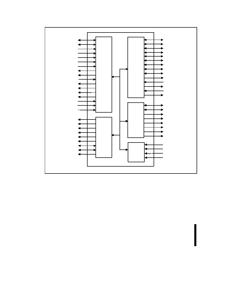
82439HX (TXC)
E
2
BE[7:0]#
DEVSEL#
PAR
REQ[3:0]#
PHLD#
PHLDA#
GNT[3:0]#
LOCK#
STOP#
IRDY#
TRDY#
FRAME#
C/BE[3:0]#
Clocks,
Reset,
and
Test
Host
Interface
D/C#
HLOCK#
HITM#
EADS#
BRDY#
BOFF#
AHOLD
NA#
KEN#/INV
CACHE#
SMIACT#
ADS#
W/R#
M/IO#
TWE#
CCS#
COE#
GWE#
CADS#
CADV#
TIO[7:0]
PCLKIN
HCLKIN
RAS[7:0]#
CAS[7:0]#
MA[11:2]
DRAM
Interface
PCI
Interface
Cache
Interface
A[31:3]
MAA[1:0]
MAB[1:0]
AD[31:0]
MWE#
BWE
RST#
TEST#
HD[63:0]
TIO[10:8]
SERR#
MPD[7:0]
MD[63:0]
055101
82439HX TXC Simplified Block Diagram

E
82439HX (TXC)
3
CONTENTS
PAGE
REVISION HISTORY...................................................................................................................................... 4
1.0. ARCHITECTURE OVERVIEW................................................................................................................. 5
2.0. SIGNAL DESCRIPTION .......................................................................................................................... 7
2.1. Host Interface....................................................................................................................................... 7
2.2. DRAM Interface ................................................................................................................................... 8
2.3. Secondary Cache Interface .................................................................................................................. 9
2.4. PCI Interface ...................................................................................................................................... 10
2.5. Clock, Reset, and Test ....................................................................................................................... 11
3.0. REGISTER DESCRIPTION ................................................................................................................... 12
3.1. I/O Control Registers.......................................................................................................................... 12
3.1.1. CONFADD
CONFIGURATION ADDRESS REGISTER ............................................................ 12
3.1.2. CONFDATA
CONFIGURATION DATA REGISTER .................................................................. 13
3.2. PCI Configuration Space Mapped Registers ...................................................................................... 14
3.2.1. PCI CONFIGURATION ACCESS ................................................................................................ 14
3.2.2. VID
VENDOR IDENTIFICATION REGISTER ........................................................................... 15
3.2.3. DID
DEVICE IDENTIFICATION REGISTER ............................................................................. 16
3.2.4. PCICMD
PCI COMMAND REGISTER ...................................................................................... 16
3.2.5. PCISTS
PCI STATUS REGISTER............................................................................................ 17
3.2.6. RID
REVISION IDENTIFICATION REGISTER ......................................................................... 17
3.2.7. CLASSC
CLASS CODE REGISTER ........................................................................................ 18
3.2.8. MLT
MASTER LATENCY TIMER REGISTER .......................................................................... 18
3.2.9. HEADT
HEADER TYPE REGISTER ........................................................................................ 19
3.2.10. BIST
BIST REGISTER............................................................................................................ 19
3.2.11. ACON
ARBITRATION CONTROL .......................................................................................... 19
3.2.12. PCON
PCI CONTROL ............................................................................................................ 20
3.2.13. CC
CACHE CONTROL REGISTER........................................................................................ 21
3.2.14. DRAMEC
DRAM EXTENDED CONTROL REGISTER ........................................................... 22
3.2.15. DRAMC
DRAM CONTROL REGISTER .................................................................................. 23
3.2.16. DRAMT
DRAM TIMING REGISTER ....................................................................................... 23
3.2.17. PAM
PROGRAMMABLE ATTRIBUTE MAP REGISTERS (PAM[6:0]) .................................... 25
3.2.18. DRB
DRAM ROW BOUNDARY REGISTERS......................................................................... 27
3.2.19. DRT
DRAM ROW TYPE REGISTER ...................................................................................... 29
3.2.20. SMRAM
SYSTEM MANAGEMENT RAM CONTROL REGISTER .......................................... 29
3.2.21. ERRCMD
ERROR COMMAND REGISTER............................................................................ 31
3.2.22. ERRSTS
ERROR STATUS REGISTER ................................................................................. 32
3.2.23. ERRSYN -- ERROR SYNDROME REGISTER......................................................................... 33

82439HX (TXC)
E
4
4.0. FUNCTIONAL DESCRIPTION .............................................................................................................. 34
4.1. Host Interface..................................................................................................................................... 34
4.2. PCI Interface ...................................................................................................................................... 34
4.3. Secondary Cache Interface ................................................................................................................ 34
4.3.1. CLOCK LATENCIES ................................................................................................................... 35
4.3.2. SNOOP CYCLES ........................................................................................................................ 36
4.3.3. CACHE ORGANIZATION............................................................................................................ 36
4.3.4. DRAM CACHE ............................................................................................................................ 37
4.4. DRAM Interface ................................................................................................................................. 38
4.4.1. DRAM ORGANIZATION.............................................................................................................. 38
4.4.2. DRAM ADDRESS TRANSLATION .............................................................................................. 42
4.4.3. DRAM TYPES ............................................................................................................................. 43
4.4.4. DRAM PERFORMANCE ............................................................................................................. 44
4.4.5. DRAM REFRESH........................................................................................................................ 46
4.4.6. SYSTEM MANAGEMENT RAM .................................................................................................. 47
4.4.7. DATA INTEGRITY SUPPORT..................................................................................................... 47
4.4.7.1. Parity .................................................................................................................................... 47
4.4.7.2. Error Detection and correction .............................................................................................. 47
4.5. PCI Bus Arbitration............................................................................................................................. 49
4.5.1. CPU POLICIES ........................................................................................................................... 50
4.6. Clock Generation and Distribution ...................................................................................................... 50
4.6.1. RESET SEQUENCING ............................................................................................................... 50
5.0. PINOUT AND PACKAGE INFORMATION ............................................................................................ 51
5.1. TXC Pinout Information ...................................................................................................................... 51
5.2. TXC Package Information .................................................................................................................. 56
6.0. TESTABILITY........................................................................................................................................ 59
6.1. NAND Tree Mode............................................................................................................................... 59
6.1.1. OVERVIEW ................................................................................................................................. 59
6.1.2. NAND CHAIN MODE .................................................................................................................. 60
6.2. ID Code Test Mode ............................................................................................................................ 65
REVISION HISTORY
Revision Date
Version
Description
July 1996
-001
Initial Release
April 1997
-002
Included information from
Specification Update
The Intel 430HX PCIset device may contain design defects or errors known as errata. Characterized errata
that may cause the 430HX's behavior to deviate from published specifications are documented in the "Intel
430HX PCIset: 82439HX (TXC) Specification Update" (Order number 297652).

E
82439HX (TXC)
5
1.0.
ARCHITECTURE OVERVIEW
The TXC interfaces with the Pentium
Æ
processor host bus, a dedicated memory data bus, and the PCI bus
(Figure 1). The TXC connects directly to the Pentium processor 3V host bus, directly to 5V or 3V DRAMs,
and directly to the 5V PCI bus. The Intel 430HX PCIset consists of the 82439HX TXC and the PCI IDE/ISA
Xcellerator (PIIX3) components. PIIX3 provides the PCI-to-ISA bridge functions along with other features
such as a fast IDE interface, Plug-n-Play port, APIC interface, Universal Serial Bus (USB) and PCI 2.1
Compliance operation.
Data Flow
Processor cycles are sent directly to the second level cache with control for the second level cache provided
by the TXC. All other processor cycles are sent to their destination (DRAM, PCI or internal TXC configuration
space) via the TXC. PCI Master cycles are sent to main memory through the TXC. The TXC performs snoop
or inquire cycles using the host bus.
ISA Bus
Pentium Processor
TXC
Main
Memory
(DRAM)
Address
Data
Control
Data
Addr
Cntl
Control
Address/Data
PCI Bus
Host Bus
Cntl
PCI
Device(s)
Cache
(SRAM)
Æ
Second Level
Cache
Tag Cntl
TIO[7:0]
ISA
Device(s)
Fast IDE
Hard
Disk
CD ROM
PIIX3
Tag
USB
1
USB
2
Universal Serial Bus
3.3V
TIO[10:8]
ECC
055102
Figure 1. TXC System Block Diagram