
PRELIMINARY
Information in this document is provided in connection with Intel products. No license, express or implied, by estoppel or otherwise, to any intellectual property rights
is granted by this document or by the sale of Intel products. Except as provided in Intel's Terms and Conditions of Sale for such products, Intel assumes no liability
whatsoever, and Intel disclaims any express or implied warranty, relating to sale and/or use of Intel products including liability or warranties relating to fitness for a
particular purpose, merchantability, or infringement of any patent, copyright or other intellectual property right. Intel products are not intended for use in medical, life
saving, or life sustaining applications. Intel retains the right to make changes to specifications and product descriptions at any time, without notice. The Intel 440FX
PCIset may contain design defects or errors known as errata. Current characterized errata are available on request. Third-party brands and names are the property
of their respective owners.
© INTEL CORPORATION 1996
May 1996
Order Number: 290549-001
Supports the Pentium
Æ
Pro Processors
at Bus Frequencies Up To 66 Mhz
Supports 32-Bit Addressing
Optimized in-Order and Request
Queue
Full Symmetric Multi-Processor
(SMP) Protocol for up to Two
Processors
Dynamic Deferred Transaction
Support
GTL+ Compliant Host Bus
Supports USWC Cycles
Integrated DRAM Controller
8 MB to 1 GB Main Memory
64/72-Bit Non-Interleaved Path to
Memory
FPM (Fast Page Mode), EDO
(Extended Data Out -Page Mode),
BEDO (Extended Data Out -Burst
Mode) DRAMs Providing x-222 to
x-4-4-4 Burst Capability
Support for Auto Detection of
Memory Type: BEDO, EDO or FPM
8 RAS Lines Available
Support for 4-, 16- and 64-Mb DRAM
Devices
Support for Symmetrical and
Asymmetrical DRAM Addressing
Configurable Support for ECC or
Parity
ECC with Single Bit Error
Correction and Multiple Bit Error
Detection
Read-Around-Write Support for
Host and PCI DRAM Read Accesses
Supports 3.3V or 5V DRAMs
PCI Bus Interface
PCI Rev. 2.1, 5V Interface Compliant
Greater than 100 MBps Data
Streaming for PCI to DRAM
Accesses Enables Native Signal
Processing (NSP) on Systems
Designed With the Pentium Pro
Processor
Integrated Arbiter With Multi-
Transaction PCI Arbitration
Accelerator Hooks
5 PCI Bus Masters are Supported in
Addition to the Host and PCI-to-ISA
I/O Bridge
Delayed Transaction Support
PCI Parity Checking and Generation
Support
Supports Concurrent Pentium Pro
and PCI Transactions to Main
Memory
Data Buffering For Increased
Performance
Extensive CPU-to-DRAM and PCI-
to-DRAM Write Data Buffering
Write Combining Support for CPU-
to-PCI Burst Writes
System Management Mode (SMM)
Compliant
208-Pin PQFP PCI Bridge/ Memory
Controller (PMC), 208-Pin PQFP for the
440FX PCIset Data Bus Accelerator
(DBX)
The Intel 440FX PCIset provides a highly integrated solution for systems based on one or two Pentium
Æ
Pro
processors. The 440FX PCIset consists of the 82441FX PCI and Memory Controller (PMC), the 82442FX Data
Bus Accelerator (DBX), and the 82371SB PCI I/O IDE Xcelerator (PIIX3). The PMC and DBX provide a two-chip
host-to-PCI bridge including the DRAM control function, the PCI interface, and the PCI arbiter function. The
440FX PCIset supports EDO, FPM, and BEDO DRAM technologies. The DRAM controller provides support for
up to eight rows of memory and optional DRAM error detection/correction or parity. The 440FX PCIset contains
extensive buffering between all interfaces for high system data throughput and concurrent operations.
INTEL 440FX PCISET
82441FX PCI AND MEMORY CONTROLLER
(PMC) AND 82442FX DATA BUS
ACCELERATOR (DBX)
82441FX (PMC) AND 82442FX (DBX)
2
PRELIMINARY
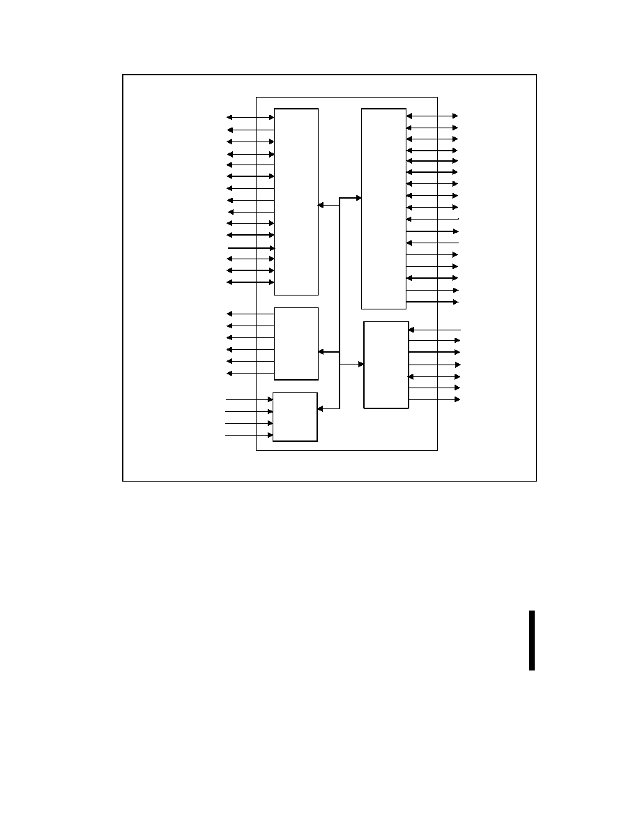
INIT#
DEVSEL#
PAR
REQ[4:0]#
PHLD#
PHLDA#
GNT[4:0]#
PLOCK#
STOP#
IRDY#
TRDY#
FRAME#
C/BE[3:0]#
HLAD#
MLAD
PC[8:0]
PD[15:0]
DDRDY#
DBX_ERR#
Clocks
And
Misc.
Host
Interface
BNR#
RS[2:0]#
FLUSH#
DRDY#
DEFER#
HIT#
HITM
HLOCK#
HREQ[4:0]#
HTRDY#
ADS#
DBSY#
BPRI#
MA[11:2]
RAS[5:0]#
MAA[1:0]
RAS[7:6]#/MAB[1:0]
WE#
PCLKIN
HCLKIN
DRAM
Interface
DBX
Interface
PCI
Interface
HA[31:3]#
PCIRST#
AD[31:0]
CAS[7:0]#
PERR#
SERR#
WSC#
CRESET#
PWROK
GTL_REFV
PMC_BLK
PMC Simplified Block Diagram

82441FX (PMC) AND 82442FX (DBX)
3
PRELIMINARY
HLAD#
MLAD
PC[8:0]
DDRDY#
PD[15:0]
Clocks
And
Misc.
Host
Interface
MD[63:0]
DRAM
Interface
PMC
Interface
HD[63:0]#
CPURST#
MPD[7:0]
HCLKIN
GTL_REFV
BREQ0#
CRESET#
DBX_ERR#
DBX_BLK
DBX Simplified Block Diagram

82441FX (PMC) AND 82442FX (DBX)
4
PRELIMINARY
CONTENTS
PAGE
1.0. OVERVIEW ......................................................................................................................................................6
2.0. SIGNAL DESCRIPTION ..................................................................................................................................8
2.1. PMC Signals .................................................................................................................................................9
2.1.1. HOST INTERFACE (PMC)....................................................................................................................9
2.1.2. DRAM INTERFACE (PMC) .................................................................................................................10
2.1.3. PCI INTERFACE (PMC)......................................................................................................................11
2.1.4. PCI SIDEBAND INTERFACE (PMC) ..................................................................................................12
2.1.5. DBX INTERFACE (PMC) ....................................................................................................................13
2.1.6. CLOCKS (PMC)...................................................................................................................................13
2.1.7. MISCELLANEOUS (PMC)...................................................................................................................13
2.1.8. POWER UP STRAP OPTIONS (PMC) ...............................................................................................14
2.2. DBX Signals................................................................................................................................................15
2.2.1. DRAM INTERFACE SIGNALS (DBX) .................................................................................................15
2.2.2. PMC INTERFACE SIGNALS (DBX)....................................................................................................15
2.2.3. HOST INTERFACE SIGNALS (DBX) .................................................................................................15
2.2.4. MISCELLANEOUS (DBX) ...................................................................................................................16
2.2.5. POWER UP STRAP OPTIONS (DBX)................................................................................................16
3.0. REGISTER DESCRIPTION ...........................................................................................................................17
3.1. I/O Mapped Registers .................................................................................................................................17
3.1.1. CONFADD
CONFIGURATION ADDRESS REGISTER ..................................................................18
3.1.2. CONFDATA
CONFIGURATION DATA REGISTER ........................................................................18
3.2. PCI Configuration Space Mapped Registers ..............................................................................................19
3.2.1. PCI CONFIGURATION ACCESS .......................................................................................................19
3.2.2. VID
VENDOR IDENTIFICATION REGISTER ..................................................................................21
3.2.3. DID
DEVICE IDENTIFICATION REGISTER....................................................................................21
3.2.4. PCICMD
PCI COMMAND REGISTER .............................................................................................21
3.2.5. PCISTS
PCI STATUS REGISTER ...................................................................................................22
3.2.6. RID
REVISION IDENTIFICATION REGISTER ................................................................................23
3.2.7. CLASSC
CLASS CODE REGISTER................................................................................................23
3.2.8. MLT
MASTER LATENCY TIMER REGISTER .................................................................................24
3.2.9. HEADT
HEADER TYPE REGISTER................................................................................................24
3.2.10. BIST
BIST REGISTER....................................................................................................................24
3.2.11. PMCCFG
PMC CONFIGURATION REGISTER ............................................................................25
3.2.12. DETURBO
DETURBO COUNTER REGISTER.............................................................................26
3.2.13. DBC
DBX BUFFER CONTROL......................................................................................................26
3.2.14. AXC
AUXILIARY CONTROL REGISTER ......................................................................................27
3.2.15. DRT
DRAM ROW TYPE REGISTER ............................................................................................28
3.2.16. DRAMC
DRAM CONTROL REGISTER.........................................................................................28
3.2.17. DRAMT
DRAM TIMING REGISTER .............................................................................................29
3.2.18. PAM
PROGRAMMABLE ATTRIBUTE MAP REGISTERS (PAM[6:0])..........................................30
3.2.19. DRB[0:7]
DRAM ROW BOUNDARY REGISTERS .......................................................................32

82441FX (PMC) AND 82442FX (DBX)
5
PRELIMINARY
3.2.20. FDHC
FIXED DRAM HOLE CONTROL REGISTER ....................................................................33
3.2.21. MTT
MULTI-TRANSACTION TIMER REGISTER..........................................................................34
3.2.22. CLT
CPU LATENCY TIMER REGISTER .......................................................................................34
3.2.23. SMRAM
SYSTEM MANAGEMENT RAM CONTROL REGISTER ................................................35
3.2.24. ERRCMD
ERROR COMMAND REGISTER ..................................................................................36
3.2.25. ERRSTS
ERROR STATUS REGISTER ........................................................................................37
3.2.26. TRC
TURBO RESET CONTROL REGISTER ...............................................................................38
4.0. FUNCTIONAL DESCRIPTION ......................................................................................................................39
4.1. System Address Map..................................................................................................................................39
4.1.1. MEMORY ADDRESS RANGES..........................................................................................................39
4.1.1.1. Compatibility Area .........................................................................................................................40
4.1.1.2. Extended Memory Area ................................................................................................................41
4.1.2. SYSTEM MANAGEMENT MODE (SMM) MEMORY RANGE............................................................42
4.1.3. MEMORY SHADOWING.....................................................................................................................42
4.1.4. I/O ADDRESS SPACE ........................................................................................................................42
4.2. Host Interface..............................................................................................................................................42
4.3. DRAM Interface ..........................................................................................................................................43
4.3.1. DRAM POPULATION RULES.............................................................................................................43
4.3.2. AUTO-DETECTION.............................................................................................................................45
4.3.3. DRAM ADDRESS TRANSLATION AND DECODING .......................................................................46
4.3.4. PSEUDO-ALGORITHM FOR DYNAMIC MEMORY SIZING .............................................................47
4.3.5. DATA INTEGRITY SUPPORT ............................................................................................................48
4.3.5.1. Software Requirements.................................................................................................................48
4.3.5.2. Parity Detection.............................................................................................................................48
4.3.5.3. Error Detection and correction ......................................................................................................49
4.3.5.4. ECC/Parity Test Mode ..................................................................................................................52
4.4. PCI Bus Arbitration .....................................................................................................................................53
4.5. System Clocking and Reset........................................................................................................................54
4.5.1. HOST FREQUENCY SUPPORT ........................................................................................................54
4.5.2. CLOCK GENERATION AND DISTRIBUTION....................................................................................54
4.5.3. SYSTEM RESET .................................................................................................................................54
4.5.3.1. Hard Reset ....................................................................................................................................55
4.5.3.2. Soft Reset .....................................................................................................................................57
4.5.3.3. CPU BIST......................................................................................................................................57
5.0. PINOUT AND PACKAGE SPECIFICATIONS ..............................................................................................58
5.1. PMC Pinout Information ..............................................................................................................................58
5.2. DBX Pinout Information...............................................................................................................................62
5.3. PMC & DBX Package Specifications..........................................................................................................66
6.0. TESTABILITY.................................................................................................................................................67
6.1. 82441FX (PMC) Test Modes ......................................................................................................................67
6.2. DBX Test Mode...........................................................................................................................................68

82441FX (PMC) AND 82442FX (DBX)
6
PRELIMINARY
1.0.
OVERVIEW
The 440FX PCIset consists of a host-to-PCI bridge and memory controller, and an I/O subsystem core that
allows an optimized price/performance path for the next generation of personal computers based on the Pentium
Pro processor. The host-to-PCI bridge consists of two components; the PCI Bridge/Memory Controller (PMC)
and the Data Bus Accelerator (DBX). The PMC and the DBX includes the following functions.
∑
Support for one/two Pentium Pro Processors at bus frequencies up to 66 MHz
∑
64-bit GTL+ based host bus data interface
∑
32-bit host address support
∑
32-bit PCI bus interface
∑
64/72-bit main memory interface
∑
Extensive data buffering between all interfaces for high throughput and concurrent operations
Pentium Æ Pro
Processor
PMC
MA[11:0]
Control
PD[15:0]
Control
MD[63:0]
MDP[7:0]
PC I Bridge and
Memory Con tro ller
Data Bus
Accelerator
DBX
Main Memory
8 MB to 1 GB
64
Data
Address/
Control
PCI Bus
ISA Bus
CD
ROM
Fast IDE
PIIX3
PCI ISA IDE
Accelerator
Hard
Disk
USB
Device
USB
Device
USB
Ports
ISA
Device
ISA
Slots
PCI
Device
PCI
Slots
I/O
APIC
Pentium Æ Pro
Processor
Interrupts
Host Bus
SYS_BLK
Figure 1. 440FX PCIset System Block Diagram

82441FX (PMC) AND 82442FX (DBX)
7
PRELIMINARY
The PMC and the DBX interface with the Pentium Pro processor host bus. A maximum of two Pentium Pro
processors are supported on the Pentium Pro host bus in a two processor symmetrical multi-processing
configuration. A 16-bit private data bus (PD[15:0]) operating at host frequency between the DBX and the PMC
provides a high throughput indirect interface between the DBX and PCI bus.
The PMC and the DBX host bus interfaces are designed based on the GTL+ specification. The PMC/DBX also
provides a 5.0V tolerant 3.3V main memory interface that allows support of either 5V or 3V DRAMs. The PMC
connects directly to the 5V PCI bus. The PMC includes an internal PCI arbiter.
The PIIX3 provides the PCI-to-ISA bridge functions along with Universal Serial Bus (USB) support. In addition,
the PIIX3 contains a local bus master IDE interface and an interface for the I/O APIC component required for
second Pentium Pro processor support. The PIIX3 is compliant to the PCI Rev. 2.1 specification.
Host Interface
The PMC provides bus control signals and address paths for transfers between the host bus, PCI bus, and main
memory. The PMC supports an optimized in-order queue that allows for pipelining of outstanding transaction
requests on the host bus.
During Host to PCI cycles, the PMC controls the PCI protocol and data flows through the DBX and PMC via the
private bus (PD[15:0]). This bus operates at the host bus clock frequency.
The PMC also receives addresses from PCI bus initiators for PCI-to-DRAM transfers. These addresses are
translated to the appropriate memory addresses and are also provided on the host bus for snoop cycles. PCI
master cycles are sent to main memory through the PMC with data moving over the PD bus to the DBX, which
subsequently forwards the data to DRAM.
DRAM Interface
The PMC integrates a main memory controller that supports a 64/72-bit DRAM interface. The PMC DRAM
controller interface supports the following features:
∑
DRAM type: standard Fast Page Mode(FPM), Extended Data Out (EDO) (sometimes referred to as Hyper
Page Mode) and Burst EDO (BEDO) memory.
∑
Memory Size: 8 Mbytes to 1 Gbytes with eight RAS lines available.
∑
Addressing Type: Symmetrical and Asymmetrical addressing
∑
Memory Modules supported: Single and double density SIMMs and DIMMs
∑
DRAM device technology: 4 Mbit, 16 Mbit, and 64 Mbit
∑
DRAM Speeds: 50, 60, and 70 ns
The memory controller provides capability for auto-detection of BEDO/EDO/FPM DRAM type installed in the
system during system configuration and initialization providing a Plug and Play DRAM interface to the user. The
PMC/DBX also provides data integrity features including ECC in the memory array and parity error detection.
During host and PCI reads of the DRAM, the DBX provides error checking and correction of the data. The DBX
supports multiple-bit error detection and single-bit error correction when ECC mode is enabled and parity error
detection when parity mode is enabled. During host or PCI master writes to DRAM, the DBX generates
ECC/Parity for the data.

82441FX (PMC) AND 82442FX (DBX)
8
PRELIMINARY
DBX
A single DBX provides a 64-bit CPU-to-main memory data path. The DBX also interfaces to the 16-bit private
data bus for PCI transactions and PMC configuration register set access. The private bus operating at host
frequency provides enough throughput to sustain PCI bandwidth. The DBX allows for a cost effective solution
providing optimal CPU-to-DRAM performance while maintaining a relatively small footprint (208 pins).
PCI Interface
The PCI interface is 5V Revision 2.1 compliant and supports up to five PCI bus masters in addition to the PIIX3
components. The PMC supports a divide-by-2 synchronous PCI coupling to the host bus frequency.
IOAPIC
The IOAPIC component supports dual processors as well as enhanced interrupt processing in the single
processor environment. No special interface is required on the PMC in this case. The PMC furnishes an external
status output signal to the standalone IOAPIC component that is used for buffer flushing during synchronization
events for the PIIX3.
2.0.
SIGNAL DESCRIPTION
This section provides a detailed description of each signal. The signals are arranged in functional groups
according to their associated interface.
The "#" symbol at the end of a signal name indicates that the active, or asserted state occurs when the signal is
at a low voltage level. When "#" is not present after the signal name the signal is asserted when at the high
voltage level.
The terms assertion and negation are used extensively. This is done to avoid confusion when working with a
mixture of "active-low" and "active-high" signals. The term assert, or assertion indicates that a signal is active,
independent of whether that level is represented by a high or low voltage. The term negate, or negation
indicates that a signal is inactive.
The following notations are used to describe the signal and type:
I
Input pin
O
Output pin
OD
Open Drain Output pin. This requires a pull-up to the VCC of the processor core
I/O
Bi-directional Input/Output pin
The signal description also includes the type of buffer used for the particular signal:
GTL+ Open Drain GTL+ interface signal. Refer to the GTL+ I/O Specification for complete details
PCI
PCI bus interface signals. These signals are compliant with the PCI 5.0V Signaling Environment DC
and AC Specifications
LVTTL Low Voltage TTL compatible signals. These are also 3.3V outputs with 5V tolerant inputs.

82441FX (PMC) AND 82442FX (DBX)
9
PRELIMINARY
2.1.
PMC Signals
2.1.1.
HOST INTERFACE (PMC)
Name
Type
Description
INIT#
O
LVTTL
INITIALIZATION: INIT# is asserted (soft reset) by the PMC during a CPU shutdown
bus cycle, or after the writing to the reset control register to initiate a soft reset.
HA[31:3]#
I/O
GTL+
ADDRESS BUS: HA[31:3]# connects to the CPU address bus. The PMC drives
HA[31:3]# during snoop cycles on behalf of PCI initiators. Note that the CPU
address bus is an inverted bus.
ADS#
I/O
GTL+
ADDRESS STROBE: The CPU bus owner asserts ADS# to indicate the first of
two cycles of a request phase.
BNR#
O
GTL+
BLOCK NEXT REQUEST: Used to block the current request bus owner from
issuing new requests. This signal is used to dynamically control the CPU bus
pipeline depth.
BPRI#
O
GTL+
PRIORITY AGENT BUS REQUEST: The owner of this signal will always be the
next bus owner. This signal has priority over symmetric bus requests and causes
the current symmetric owner to stop issuing new transactions unless the HLOCK#
signal is asserted. The PMC drives this signal to gain control of the CPU bus.
DBSY#
I/O
GTL+
DATA BUS BUSY: Used by the data bus owner to hold the data bus for transfers
requiring more than one cycle.
DEFER#
O
GTL+
DEFER: The PMC uses a dynamic deferring policy to optimize for system
performance. The PMC also uses the DEFER# signal to indicate a CPU retry
response.
DRDY#
I/O
GTL+
DATA READY: Asserted for each cycle that data is transferred.
FLUSH#
OD
LVTTL
FLUSH: Issued to CPU(s) for L1/L2 cache for a write back of all cache lines in
modified state and then invalidate all cache lines. This signal is asserted by the
PMC to throttle the CPU bus in the deturbo mode of operation.
HIT#
I/O
GTL+
HIT: Indicates that a caching agent holds an unmodified version of the requested
line. Also, driven in conjunction with HITM#, by the target, to extend the snoop
window.
HITM#
I/O
GTL+
HIT MODIFIED: Indicates that a caching agent holds a modified version of the
requested line and that this agent assumes responsibility for providing the line.
Also, driven in conjunction with HIT# to extend the snoop window.
HLOCK#
I
GTL+
HOST LOCK: All CPU bus cycles sampled with the assertion of HLOCK# and
ADS#, until the negation of HLOCK# must be atomic (i.e., no PCI activity to DRAM
is allowed and the locked cycle is translated to PCI, if targeted for the PCI bus.)
HREQ[4:0]#
I/O
GTL+
REQUEST COMMAND: Asserted during both clocks of the request phase. In the
first clock, the signals define the transaction type to a level of detail that is sufficient
to begin a snoop request. In the second clock, the signals carry additional
information to define the complete transaction type.
HTRDY#
I/O
GTL+
HOST TARGET READY: Indicates that the target of the CPU transaction is able to
enter the data transfer phase.

82441FX (PMC) AND 82442FX (DBX)
10
PRELIMINARY
Name
Type
Description
RS[2:0]#
I/O
GTL+
RESPONSE SIGNALS: Indicates the type of response:
RS[2:0] Response type
000 Idle state
001 Retry response
010 Defer response
011 Reserved
100 Hard Failure
101 Normal without data
110 Implicit Writeback
111 Normal with data
Note: All of the signals in the host interface are described in the Pentium Pro datasheet. The preceding table
highlights 440FX PCIset specific uses of these signals.
2.1.2.
DRAM INTERFACE (PMC)
Name
Type
Description
CAS[7:0]#
O
LVTTL
COLUMN ADDRESS STROBE: The CAS[7:0]# signals are used to latch the column
address on the MA[11:0] lines into the DRAMs. These signals drive the DRAM array
directly without external buffering.
MA[11:2]
O
LVTTL
MEMORY ADDRESS: MA[11:2] provide multiplexed row and column address to
DRAM. MA[11:2] are externally buffered to drive the address lines of the DRAM.
MAA[1:0]
O
LVTTL
LOWER MEMORY ADDRESS SET A: MAA[1:0] are the lower two bits of the memory
address used to complete the row and column address to the DRAM. These two pins
are toggled during the burst phase.
RAS[7:6]#/
MAB[1:0]
O
LVTTL
ROW ADDRESS STROBES RAS7# AND RAS6# OR LOWER MEMORY
ADDRESS SET B: MAB[1:0] are the lower two bits of the memory address used to
complete the row and column address to the DRAM. These signals are toggled during
the burst phase. RAS[7:6]# are used to latch the row address on the MA[11:0] lines
into the DRAMs. These signals should be used to select the upper two rows in the
memory array. These signals drive the DRAM array directly without external buffers.
The strapping on PC8 selects the function of these pins.
RAS[5:0]#
O
LVTTL
ROW ADDRESS STROBE: The RAS[5:0]# signals are used to latch the row address
on the MA[11:0] lines into the DRAMs. Each signal is used to select one DRAM row.
These signals drive the DRAM array directly without any external buffers.
WE#
O
LVTTL
WRITE ENABLE SIGNAL: WE# is asserted during writes to main memory. During
burst writes to main memory, WE# is externally buffered to drive the WE# inputs of the
DRAM.

82441FX (PMC) AND 82442FX (DBX)
11
PRELIMINARY
2.1.3.
PCI INTERFACE (PMC)
Name
Type
Description
AD[31:0]
I/O
PCI
PCI ADDRESS/DATA: These signals are connected to the PCI address/data bus.
Address is driven by the PMC with FRAME# assertion, data is driven or received in
following clocks.
DEVSEL#
I/O
PCI
DEVICE SELECT: Device select, when asserted, indicates that a PCI target device
has decoded its address as the target of the current access. The PMC asserts
DEVSEL# based on the DRAM address range being accessed by a PCI initiator or if it
decodes the current configuration cycle is targeted to the PMC.
FRAME#
I/O
PCI
FRAME: FRAME# is an output when the PMC acts as an initiator on the PCI Bus.
FRAME# is asserted by the PMC to indicate the beginning and duration of an access.
The PMC asserts FRAME# to indicate a bus transaction is beginning.
IRDY#
I/O
PCI
INITIATOR READY: IRDY# is an output when PMC acts as a PCI initiator and an
input when the PMC acts as a PCI target. The assertion of IRDY# indicates the
current PCI Bus initiator's ability to complete the current data phase of the transaction.
PLOCK#
I/O
PCI
PLOCK: PLOCK# indicates an exclusive bus operation and may require multiple
transactions to complete. When PLOCK# is asserted, non-exclusive transactions may
proceed. A grant to start a transaction on the PCI Bus does not guarantee control of
the PLOCK# signal. Control of the PLOCK# signal is obtained under its own protocol
in conjunction with the GNT# signal. The PMC supports bus lock mode of operation.
TRDY#
I/O
PCI
TARGET READY: TRDY# is an input when the PMC acts as a PCI initiator and an
output when the PMC acts as a PCI target. The assertion of TRDY# indicates the
target agent's ability to complete the current data phase of the transaction.
C/BE[3:0]#
I/O
PCI
COMMAND/BYTE ENABLE: PCI Bus Command and Byte Enable signals are
multiplexed on the same pins. During the address phase of a transaction, C/BE[3:0]#
define the bus command. During the data phase C/BE[3:0]# are used as byte enables.
The byte enables determine which byte lanes carry meaningful data. PCI Bus
command encoding and types are listed below.
C/BE[3:0]#
Command Type
0 0 0 0
Interrupt Acknowledge
0 0 0 1
Special Cycle
0 0 1 0
I/O Read
0 0 1 1
I/O Write
0 1 0 0
Reserved
0 1 0 1
Reserved
0 1 1 0
Memory Read
0 1 1 1
Memory Write
1 0 0 0
Reserved
1 0 0 1
Reserved
1 0 1 0
Configuration Read
1 0 1 1
Configuration Write
1 1 0 0
Memory Read Multiple
1 1 0 1
Reserved (Dual Address Cycle)
1 1 1 0
Memory Read Line
1 1 1 1
Memory Write and Invalidate

82441FX (PMC) AND 82442FX (DBX)
12
PRELIMINARY
Name
Type
Description
PAR
I/O
PCI
PARITY: PAR is driven by the PMC when it acts as a PCI initiator during address and
data phases for a write cycle, and during the address phase for a read cycle. PAR is
driven by the PMC when it acts as a PCI target during each data phase of a PCI
memory read cycle. Even parity is generated across AD[31:0] and C/BE[3:0]#.
PERR#
I/O
PCI
PCI PARITY ERROR: Pulsed by an agent receiving data with bad parity one clock
after PAR is asserted. The PMC generates PERR# active if it detects a parity error
on the PCI bus and the PERR# Enable bit is set.
SERR#
O
PCI
SYSTEM ERROR: The PMC can be programmed to assert SERR# for 2 types of
memory error conditions:
1. Main memory single bit ECC error
2. Main memory (DRAM) parity or multiple bit ECC error
The PMC can be programmed to assert SERR# when it detects a target abort on a
PMC initiated PCI cycle and when PERR# is sampled active.
PCIRST#
O
PCI
PCI RESET: PCI bus reset forces the PCI interfaces of each device to a known
state. The PMC generates a minimum 1 ms pulse for PCIRST#.
STOP#
I/O
PCI
STOP: STOP# is an input when the PMC acts as a PCI initiator and an output when
the PMC acts as a PCI target. STOP# indicates that the bus initiator must
immediately terminate its current PCI Bus cycle at the next clock edge and release
control of the PCI Bus. STOP# is used for disconnect, retry, and abort sequences on
the PCI Bus.
2.1.4.
PCI SIDEBAND INTERFACE (PMC)
Name
Type
Description
PHOLD#
I
PCI
PCI HOLD: The PIIX3 asserts this signal to request the PCI bus.
PHLDA#
O
PCI
PCI HOLD ACKNOWLEDGE: The PMC asserts this signal to grant PCI bus
ownership to the PIIX3.
WSC#
O
PCI
WRITE SNOOP COMPLETE: Asserted to indicate that all that the snoop activity on
the CPU bus on behalf of the last PCI-to-DRAM write transaction is complete.
REQ[4:0]#
I
PCI
PCI BUS REQUEST: REQ[4:0]# are the PCI bus request signals used by the PMC
for PCI initiator arbitration.
GNT[4:0]#
O
PCI
PCI GRANT: GNT[4:0]# are the PCI bus grant signals used by the PMC for PCI
initiator arbitration.

82441FX (PMC) AND 82442FX (DBX)
13
PRELIMINARY
2.1.5.
DBX INTERFACE (PMC)
Name
Type
Description
DBX_ERR#
I
LVTTL
DBX ERROR: Asserted by the DBX if an ECC or parity error occurred during a
memory cycle. DBX_ERR# is asserted for 5 host clocks to indicate a Single-bit ECC
error and 6 host clocks to indicate a parity or Multi-bit ECC error.
HLAD#
O
LVTTL
HOST LATCH AND ADVANCE: During CPU reads (both from DRAM and PCI), this
signal controls the latching of the read data into the DBX CPU interface output latch.
MLAD
O
LVTTL
MEMORY LATCH AND ADVANCE: During DRAM reads, asserting this signal
latches memory read data into the DBX. During DRAM writes, asserting this signal
latches write data out of the DBX.
PC[8:0]
I/O
LVTTL
PMC CONTROL SIGNALS: PC[8:0] are control signals between the PMC and DBX.
PD[15:0]
I/O
LVTTL
PRIVATE DATA BUS: This is a 16 bit private data path between the PMC and DBX.
This bus runs at the host clock rate and is used to transfer data during CPU-to-PCI
cycles and PCI to DRAM cycles
DDRDY#
O
LVTTL
DELAYED DATA READY: This delayed version of the DRDY# signal is asserted by
the PMC to the DBX.
2.1.6.
CLOCKS (PMC)
Name
Type
Description
HCLKIN
I
2.5V
LVTTL
HOST CLOCK IN: This pin receives a host clock input from an external clock source.
The input is configurable via the PD1 strap. If the PD1 is sampled low at reset(default),
3.3V buffer mode is enabled. This is normal operation enabled by internal pulldowns. If
PD1 is sampled high, 2.5V buffer mode is enabled.
PCLKIN
I
LVTTL
PCI CLOCK IN: This pin receives a PCI clock reference that is synchronous with
respect to the host clock. This is the PCI clock reference that can be synchronously
derived by an external clock synthesizer component from the host clock (divide-by-2).
This signal clocks the PMC logic that is in the PCI clock domain.
2.1.7.
MISCELLANEOUS (PMC)
Name
Type
Description
CRESET#
O
LVTTL
CHIP RESET: This is a reset output signal driven by the PMC to the DBX. CRESET#
is driven active for 2 msec. The DBX drives CPURST# to the CPUs, which is a 2 host
clocks delayed version of the CRESET#. The PMC can also activate CRESET#
under software control by writing to the internal reset configuration regsiter to initiate a
hard reset or CPU BIST.
GTL_REFV
I
GTL+ REFERENCE VOLTAGE: This is the reference voltage derived from the
termination voltage to the pullup resistors and determines the noise margin for the
signals.

82441FX (PMC) AND 82442FX (DBX)
14
PRELIMINARY
Name
Type
Description
PWROK
I
LVTTL
POWER OK: This input goes active after all the power supplies in the system have
reached their specified values. PWROK forces all of the PMC internal state machines
to their default values. PWROK inactive generates CPURST# and PCIRST# active.
The rising edge of PWROK is asynchronous, but must meet set-up and hold
specifications for recognition on any specific clock. The PMC holds CPURST# for 2
msec and PCIRST# active for 1 msec after the rising edge of PWROK.
2.1.8.
POWER UP STRAP OPTIONS (PMC)
Below is a list of all power on options that are loaded into the PMC based on the voltage level present on the
respective strappings at the rising edge of PWROK. The PMC floats all signals connected to straps during
CRESET# and keeps them floated for a minimum of 4 host clocks after the negation of CRESET#. To enable the
different modes, external pullups should be approximately 10 K
to 3.3V (does not apply to A7#). Note that all
signals that are used to select powerup strap options are connected to weak internal pulldowns.
Signal
Register
Name/bit
Description
PC8
PMCCFG[14]
Rows 7 And 8 Enable: PC8 selects if RAS[7:6]#/ MAB[1:0] pins are used as
row selects or extra copies of the lower two memory addresses. These are
selected as follows:
PC8
RAS[7:6]/MAB[1:0]
0
MAB[1:0]
1
RAS[7:6]#
PC[3:2]
PMCCFG[9:8]
Host Frequency Select: PC[3:2] selects the CPU bus frequency.
PC[3:2]
CPU Bus Frequency
0 0
Reserved
0 1
60 MHz
1 0
66 MHz
1 1
Reserved
PD[15:12]
Test Mode: See Testability Section
PD1
HCLKIN Input Buffer Select: PD1 selects whether the 2.5V or 3.3V mode is
enabled.
PC1
HCLKIN Input Buffer Select
0
3.3V Input (Default)
1
2.5V Input
A7#
PMCCFG2
In-order Queue Depth Select/Enable: The value on A7# sampled on the
rising edge of CRESET# reflects if the IOQD is set to 1 or maximum of four.
Note that A7# is pulled up as a GTL+ signal and can be driven by to zero by
external logic.

82441FX (PMC) AND 82442FX (DBX)
15
PRELIMINARY
2.2.
DBX Signals
2.2.1.
DRAM INTERFACE SIGNALS (DBX)
Name
Type
Description
MD[63:0]
I/O
LVTTL
MEMORY DATA: These signals are connected to the DRAM data bus and have weak
internal pulldowns.
MPD[7:0]
I/O
LVTTL
MEMORY PARITY DATA: These signals are connected to the parity or ECC bits of the
DRAM data bus and have weak internal pulldowns.
2.2.2.
PMC INTERFACE SIGNALS (DBX)
Name
Type
Description
DBX_ERR#
O
LVTTL
DBX ERROR: DBX_ERR# is generated for ECC or parity errors during a memory
read cycle. DBX_ERR# is asserted for 5 host clocks to indicate a Single-bit ECC
error and 6 host clocks to indicate a parity or Multi-bit ECC error.
HLAD#
I
LVTTL
HOST LATCH AND ADVANCE SIGNAL: During CPU reads, HLAD# controls the
latching of read data into the DBX CPU interface output latch.
MLAD
I
LVTTL
MEMORY LATCH AND ADVANCE SIGNAL: During DRAM reads, the PMC
asserts this signal to latch memory read data into the DBX. During DRAM writes,
the PMC asserts this signal to latch write data from the DBX.
PC[8:0]
I
LVTTL
PMC DBX CONTROL SIGNALS: PC[8:0] are control signals between the PMC and
DBX.
DDRDY#
I
LVTTL
DELAYED DATA READY: The PMC asserts this delayed version of DRDY# to the
DBX.
PD[15:0]
I/O
LVTTL
PRIVATE DATA BUS: These signals are connected to the PD data bus on the
PMC. This is the data path for the PCI-to-DRAM and CPU-to-PCI cycles. During
PCI-to-DRAM reads and CPU-to-PCI writes, the DBX drives data on this bus.
During CPU-to-PCI reads and PCI-to-DRAM writes, the DBX receives data on this
bus.
2.2.3.
HOST INTERFACE SIGNALS (DBX)
Name
Type
Description
HD[63:0]#
I/O
GTL+
HOST DATA: These signals are connected to the CPU data bus. Note that the data
signals are inverted on the CPU bus.
CPURST#
O
GTL+
CPU RESET: The CPURST# pin is an output from the DBX that is driven directly from
the CRESET#. It allows the CPUs to begin execution at a known state.

82441FX (PMC) AND 82442FX (DBX)
16
PRELIMINARY
2.2.4.
MISCELLANEOUS (DBX)
Name
Type
Description
HCLKIN
I
2.5V
LVTTL
HOST CLOCK IN: This pin receives a host clock input from an external source. The
input is configurable via the PD1 strap. If the PD1 is sampled low at reset (default),
3.3V buffer mode is enabled. This is normal operation enabled by internal pulldowns.
If PD1 is sampled high, 2.5V buffer mode is enabled.
CRESET#
I
LVTTL
CHIP RESET: This is a reset input signal driven by the PMC to the DBX. It forces the
DBX to begin execution in a known state. This signal is also used to drive the
CPURST# to the CPUs.
GTL_REFV
I
GTL REFERENCE VOLTAGE: This is the reference voltage derived from the
termination voltage to the pullup resistors and determines the noise margin for the
signals. This signal goes the reference input of the GTL+ sense amp on each GTL+
input or I/O pin.
BREQ0#
O
GTL+
SYMMETRIC AGENT BUS REQUEST: Driven by the DBX during CPURST# to
configure the symmetric bus agents.
2.2.5.
POWER UP STRAP OPTIONS (DBX)
Below is a list of all power on options that are loaded into the DBX, based on the voltage level present on the
respective strappings at the rising edge of CRESET#. To enable the different modes, external pullups should be
approximately 10 K
to 3.3V. Note that all signals that are used to select powerup strap options are connected
to weak internal pulldowns.
Signal
Register
Name/bit
Description
PD[5:2]
Test Mode: See Testability Section
PD1
HCLKIN Input Buffer Select: PD1 selects whether the 2.5V or 3.3V mode is enabled.
PC1
HCLKIN Input Buffer Select
0
3.3V Input (Default)
1
2.5V Input

82441FX (PMC) AND 82442FX (DBX)
17
PRELIMINARY
3.0.
REGISTER DESCRIPTION
The PMC contains two sets of software accessible registers (I/O Mapped and Configuration registers), accessed
via the Host CPU I/O address space. The I/O Mapped registers control access to PCI configuration space.
Configuration Registers reside in PCI configuration space and specify PCI configuration, DRAM configuration,
operating parameters, and optional system features.
The PMC internal registers (both I/O Mapped and Configuration registers) are accessible by the Host CPU. The
registers can be accessed as Byte, Word (16-bit), or Dword (32-bit) quantities, with the exception of CONFADD
which can only be accessed as a Dword. All multi-byte numeric fields use "little-endian" ordering (i.e., lower
addresses contain the least significant parts of the field). The following nomenclature is used for access
attributes.
RO
Read Only. If a register is read only, writes to this register have no effect.
R/W
Read/Write. A register with this attribute can be read and written.
R/WC
Read/Write Clear. A register bit with this attribute can be read and written. However, a write of 1
clears (sets to 0) the corresponding bit and a write of 0 has no effect.
Some of the PMC registers described in this section contain reserved bits. Software must deal correctly with
fields that are reserved. On reads, software must use appropriate masks to extract the defined bits and not rely
on reserved bits being any particular value. On writes, software must ensure that the values of reserved bit
positions are preserved. That is, the values of reserved bit positions must first be read, merged with the new
values for other bit positions and then written back.
In addition to reserved bits within a register, the PMC contains address locations in the PCI configuration space
that are marked "Reserved" (Table 3-1). The PMC responds to accesses to these address locations by
completing the host cycle. When a reserved register location is read, a zero value is returned. Software should
not write to reserved PMC configuration locations in the device-specific region (above address offset 3Fh).
During a hard reset, the PMC sets its internal configuration registers to predetermined default states. The
default state represents the minimum functionality feature set required to successfully bring up the system.
Hence, it does not represent the optimal system configuration. It is the responsibility of the system initialization
software (usually BIOS) to properly determine the DRAM configurations, operating parameters and optional
system features that are applicable, and to program the PMC registers accordingly.
Note:
The 440FX PCIset depends on the atomicity of configuration cycles in a 2-way SMP system. Thus,
software (BIOS or OS) must guarantee that in a system with two processors only one processor can
access the configuration space at any time. During system initialization, only the "Boot Processor" must
be allowed access to configuration space. Additionally, PnP BIOS and EISA configuration utilities must
guarantee that addresses 0CF8h to 0CFFh are allocated as motherboard addresses and not available
as I/O locations.
3.1.
I/O Mapped Registers
The PMC contains two registers that reside in the CPU I/O address space--the Configuration Address
(CONFADD) Register and the Configuration Data (CONFDATA) Register. The Configuration Address Register
enables/disables the configuration space and determines what portion of configuration space is visible through
the Configuration Data window.

82441FX (PMC) AND 82442FX (DBX)
18
PRELIMINARY
3.1.1.
CONFADD
CONFIGURATION ADDRESS REGISTER
I/O Address:
0CF8h (Accessed as a Dword)
Default Value:
00000000h
Access:
Read/Write
CONFADD is a 32-bit register accessed only when referenced as a Dword. A Byte or Word reference will "pass
through" the Configuration Address Register to the PCI Bus. The CONFADD Register contains the Bus Number,
Device Number, Function Number, and Register Number for which a subsequent configuration access is
intended.
Bit
Descriptions
31
Configuration Enable (CONE). 1=Enable. 0=Disable.
30:24
Reserved.
23:16
Bus Number (BUSNUM). When BUSNUM is programmed to 00h, the target of the configuration
cycle is either the PMC or the PCI Bus that is directly connected to the PMC, depending on the Device
Number field. If the Bus Number is programmed to 00h and the PMC is not the target, a type 0
configuration cycle is generated on PCI. If the Bus Number is non-zero, a type 1 configuration cycle is
generated on PCI with the Bus Number mapped to AD[23:16] during the address phase.
15:11
Device Number (DEVNUM). This field selects one agent on the PCI Bus selected by the Bus
Number. During a Type 1 Configuration cycle, this field is mapped to AD[15:11]. During a Type 0
configuration cycle, this field is decoded and one of AD[31:11] is driven to 1. The PMC is always
Device Number 0.
10:8
Function Number (FUNCNUM). This field is mapped to AD[10:8] during PCI configuration cycles.
This allows the configuration registers of a particular function in a multi-function device to be accessed.
The PMC responds to configuration cycles with a function number of 000b; all other function number
values attempting access to the PMC (Device Number = 0, Bus Number = 0) generate a type 0
configuration cycle on the PCI Bus with no IDSEL asserted, which results in a master abort.
7:2
Register Number (REGNUM). This field selects one register within a particular bus, device, and
function as specified by the other fields in the Configuration Address Register. This field is mapped to
AD[7:2] during PCI configuration cycles.
1:0
Reserved.
3.1.2.
CONFDATA
CONFIGURATION DATA REGISTER
I/O Address:
0CFCh
Default Value:
00000000h
Access:
Read/Write
CONFDATA is a 32-bit read/write window into configuration space. The portion of configuration space that is
referenced by CONFDATA is determined by the contents of CONFADD.
Bit
Descriptions
31:0
Configuration Data Window (CDW). If bit 31 of CONFADD is 1, any I/O reference in the
CONFDATA I/O space is mapped to configuration space using the contents of CONFADD.

82441FX (PMC) AND 82442FX (DBX)
19
PRELIMINARY
3.2.
PCI Configuration Space Mapped Registers
The PCI Bus defines a slot based "configuration space" that allows each device to contain up to 256 8-bit
configuration registers. The PCI specification defines two bus cycles to access the PCI configuration space
Configuration Read and Configuration Write. While memory and I/O spaces are supported by the Pentium
microprocessor, configuration space is not supported. The PCI specification defines two mechanisms to access
configuration space, Mechanism #1 and Mechanism #2. The PMC only supports Mechanism #1 (both type 0 and
1 accesses). Table 1 shows the PMC configuration space.
The configuration access mechanism makes use of the CONFADD Register and CONFDATA Register. To
reference a configuration register, a Dword I/O write cycle is used to place a value into CONFADD that specifies
the PCI Bus, the device on that bus, the function within the device, and a specific configuration register of the
device function being accessed. CONFADD[31] must be 1 to enable a configuration cycle. Then, CONFDATA
becomes a window onto four bytes of configuration space specified by the contents of CONFADD. Read/write
accesses to CONFDATA generates a PCI configuration cycle to the address specified by CONFADD.
3.2.1.
PCI CONFIGURATION ACCESS
Type 0 Access: If the Bus Number field of CONFADD is 0, a type 0 configuration cycle is generated on PCI.
CONFADD[10:2] is mapped directly to AD[10:2]. The Device Number field of CONFADD is decoded onto
AD[31:11]. The PMC is Device #0 and does not pass its configuration cycles to PCI. Thus, AD11 is never
asserted. (For accesses to device #1, AD12 is asserted, etc., to Device #20 which asserts AD31.) Only one AD
line is asserted at a time. All device numbers higher than 20 cause a type 0 configuration access with no IDSEL
asserted, which results in a master abort.
Type 1 Access: If the Bus Number field of CONFADD is non-zero, a type 1 configuration cycle is generated on
PCI. CONFADD[23:2] are mapped directly to AD[23:2]. AD[1:0] are driven to 01 to indicate a Type 1
Configuration cycle. All other lines are driven to 0.

82441FX (PMC) AND 82442FX (DBX)
20
PRELIMINARY
Table 1. PMC Configuration Space
Address
Offset
Register
Symbol
Register Name
Access
00
-
01h
VID
Vendor Identification
RO
02
-
03h
DID
Device Identification
RO
04
-
05h
PCICMD
PCI Command Register
R/W
06
-
07h
PCISTS
PCI Status Register
RO, R/WC
08
RID
Revision Identification
RO
09
-
0Bh
CLASSC
Class Code
RO
0Ch
Reserved
0Dh
MLT
Master Latency Timer
R/W
0Eh
HEADT
Header Type
R/W
0Fh
BIST
BIST Register
R/W
10
-
4Fh
Reserved
50
-
51h
PMCCFG
PMC Configuration
R/W
52h
DETURBO
Deturbo Counter Control
R/W
53h
DBC
DBX Buffer Control
R/W
54h
AXC
Auxiliary Control
R/W
55
-
56h
DRAMR
DRAM Row Type
R/W
57h
DRAMC
DRAM Control
R/W
58h
DRAMT
DRAM Timing
R/W
59
-
5Fh
PAM[6:0]
Programmable Attribute Map (7 registers)
R/W
60
-
67h
DRB[7:0]
DRAM Row Boundary (8 registers)
R/W
68h
FDHC
Fixed DRAM Hole Control
R/W
69
-
6Fh
Reserved
70h
MTT
Multi-Transaction Timer
R/W
71h
CLT
CPU Latency Timer
R/W
72h
SMRAM
System Management RAM Control
R/W
73
-
8Fh
Reserved
90h
ERRCMD
Error Command Register
R/W
91h
ERRSTS
Error Status Register
R/WC
92h
Reserved
93h
TRC
Turbo Reset Control Register
R/WC
94
-
FFh
Reserved

82441FX (PMC) AND 82442FX (DBX)
21
PRELIMINARY
3.2.2.
VID
VENDOR IDENTIFICATION REGISTER
Address Offset:
00
-
01h
Default Value:
8086h
Attribute:
Read Only
The VID register contains the vendor identification number. This 16-bit register combined with the Device
Identification register uniquely identify any PCI device. Writes to this register have no effect.
Bit
Description
15:0
Vendor Identification Number. This is a 16-bit value assigned to Intel. Intel VID = 8086h.
3.2.3.
DID
DEVICE IDENTIFICATION REGISTER
Address Offset:
02
-
03h
Default Value:
1237h
Attribute:
Read Only
This 16-bit register combined with the Vendor Identification register uniquely identifies any PCI device. Writes to
this register have no effect.
Bit
Description
15:0
Device Identification Number. This is a 16 bit value assigned to the PMC.
3.2.4.
PCICMD
PCI COMMAND REGISTER
Address Offset:
04
-
05h
Default Value:
0006h
Attribute:
Read/Write
This 16-bit register provides basic control over the PMC's ability to respond to PCI cycles. The PCICMD register
enables and disables the SERR# signal, the parity error signal (PERR#), PMC response to PCI special cycles,
and enables and disables PCI master accesses to main memory.
Bit
Descriptions
15:10
Reserved.
9
Fast Back-to-Back. Not Implemented. This bit is hardwired to 0.
8
SERR# Enable (SERRE). If this bit is set to a 1, the PMC generates SERR# signal for all relevant bits
set in the ERRSTS and PCISTS registers as controlled with the corresponding bits of the ERRCMD
register. If SERRE is reset to 0, then SERR# is never driven by the PMC. Address Parity error
reporting as a target is enabled by the PERRE bit located in this register.
7
Address/Data Stepping. Not Implemented. This bit is hardwired to 0.
6
Parity Error Enable (PERRE). PERRE controls the PMC's response to PCI parity errors during data
phase when PMC receives the data. If PERRE=1, these errors are reported on the PERR# signal.
Note that, when PERRE=1, address parity errors are reported via the SERR# mechanism (if enabled
via SERRE bit). If PERRE=0, parity errors are not signaled (i.e., PMC's parity checking is disabled).

82441FX (PMC) AND 82442FX (DBX)
22
PRELIMINARY
Bit
Descriptions
5
Reserved.
4
Memory Write and Invalidate Enable. Not Implemented. This bit is hardwired to 0.
3
Special Cycle Enable. Not Implemented. This bit is hardwired to 0.
2
Bus Master Enable (BME). Not Implemented. This bit is hardwired to 1 (PMC bus master capability
always enabled).
1
Memory Access Enable (MAE). Not Implemented. This bit is hardwired to 1 (PMC allows PCI master
access to main memory).
0
I/O Access Enable (IOAE). Not Implemented. This bit is hardwired to 0 (PMC does not respond to
PCI I/O cycles).
3.2.5.
PCISTS
PCI STATUS REGISTER
Address Offset:
06
-
07h
Default Value:
0280h
Attribute:
Read Only, Read/Write Clear
PCISTS is a 16-bit status register that reports the occurrence of a PCI master abort and PCI target abort.
PCISTS also indicates the DEVSEL# timing that has been set by the PMC hardware. Bits [15:12,8] are
read/write clear and bits [10:9] are read only.
Bit
Descriptions
15
Detected Parity Error (DPE)
RW/C. This bit is set to a 1 to indicate PMC's detection of a parity error
in either the data or address phase when it is the target of the PCI cycle. Software sets this bit to 0 by
writing a 1 to it. Note that the function of this bit is not affected by the PERRE bit.
14
Signaled System Error (SSE)
RW/C. When the PMC asserts the SERR# signal, this bit is also set to
1. Software sets this bit to 0 by writing a 1 to it.
13
Received Master Abort Status (RMAS)
RW/C. When the PMC terminates a Host-to-PCI transaction
(PMC is a PCI master) with an unexpected master abort, this bit is set to 1. Note that master abort is the
normal and expected termination of PCI special cycles. Software sets this bit to 0 by writing a 1 to it.
12
Received Target Abort Status (RTAS)
RW/C. When a PMC-initiated PCI transaction is terminated
with a target abort, RTAS is set to 1. The PMC also asserts SERR# if enabled in the ERRCMD register.
Software sets this bit to 0 by writing a 1 to it.
11
Signaled Target Abort Status (STAS)
RW/C. When, as a PCI target, the PMC initiates a target abort
to terminate a PCI transaction, STAS is set to a 1. Software sets this bit to 0 by writing a 1 to it.
10:9 DEVSEL# Timing (DEVT)
RO. This 2-bit field indicates the timing of the DEVSEL# signal when the
PMC responds as a target, and is hard-wired to the value 01b (medium) to indicate the time when a valid
DEVSEL# can be sampled by the initiator of the PCI cycle.
8
Data Parity Detected (DPD)
RW/C. This bit is set to a 1, when conditions 1-3 below are met.
Software sets this bit to 0 by writing a 1 to it.
1. The PMC asserted PERR# or sampled PERR# asserted.
2. The PMC was the initiator for the operation in which the error occurred.
3. The PERRE bit in the PCI command register is set to 1
.

82441FX (PMC) AND 82442FX (DBX)
23
PRELIMINARY
Bit
Descriptions
7
Fast Back-to-Back (FB2B)
RO. This bit is hardwired to 1, since the PMC as a target supports fast
back-to-back transactions when transactions are to a different agent.
6:0
Reserved.
3.2.6.
RID
REVISION IDENTIFICATION REGISTER
Address Offset:
08h
Default Value:
xxh
Attribute:
Read Only
This register contains the revision number of the PMC. These bits are read only and writes to this register have
no effect.
Bit
Description
7:0
Revision Identification Number. This is an 8-bit value that indicates the revision identification
number for the PMC. Please refer to Specification Update or Stepping Information for RID.
3.2.7.
CLASSC
CLASS CODE REGISTER
Address Offset:
09
-
0Bh
Default Value:
060000h
Attribute:
Read Only
This register contains the device programming interface information related to the Sub-Class Code and Base
Class Code definition for the PMC. This register also contains the Base Class Code and the function sub-class
in relation to the Base Class Code.
Bit
Description
23:16
Base Class Code (BASEC): 06=Bridge device.
15:8
Sub-Class Code (SCC): 00h=Host Bridge.
7:0
Programming Interface (PI): 00h=Hardwired as a Host-to-PCI Bridge.

82441FX (PMC) AND 82442FX (DBX)
24
PRELIMINARY
3.2.8.
MLT
MASTER LATENCY TIMER REGISTER
Address Offset:
0Dh
Default Value:
00h
Attribute:
Read/Write
MLT is an 8-bit register that controls the amount of time the PMC, as a bus master, can burst data on the PCI
Bus. The Count Value is an 8 bit quantity. However, MLT[2:0] are hardwired to 0. The PMC's MLT is used to
guarantee to the PCI agents (other than PMC) a minimum amount of the system resources.
Bit
Description
7:3
Master Latency Timer Count Value. The number of clocks programmed in this field represents the
guaranteed time slice (measured in PCI clocks) allotted to the PMC, after which it must complete the
current data transfer phase and then surrender the bus as soon as its bus grant is removed. For
example, if the MLT Register is programmed to 18h, then the value is 24 PCI clocks. The default value of
MLT is 00h and disables this function.
2:0
Reserved.
3.2.9.
HEADT
HEADER TYPE REGISTER
Address Offset:
0Eh
Default:
00h
Attribute:
Read Only
This register contains the Header Type of the PMC. This code is 00h indicating that the PMC's configuration
space map follows the basic format. This register is read only.
Bit
Description
7:0
Header Type (HTYPE): 00h=Basic configuration space format.
3.2.10.
BIST
BIST REGISTER
Address Offset:
0Fh
Default:
00h
Attribute:
Read/Write
The Built In Self Test (BIST) function is not supported by the PMC. Writes to this register have no affect.
Bit
Descriptions
7:0
Reserved.

82441FX (PMC) AND 82442FX (DBX)
25
PRELIMINARY
3.2.11.
PMCCFG
PMC CONFIGURATION REGISTER
Address Offset:
50
-
51h
Default Value:
xxh (some bits reflect hardware strapping options)
Attribure:
Read/Write, Read Only
PMCCFG is a 16-bit register that is controls and logs the system level configuration.
Bit
Description
15
WSC Protocol Enable (WPE)
R/W. 1=Disable. 0=Enable(default). This bit enables WSC protocol
which is required for a two processor system using the IOAPIC. In a uniprocessor system, this bit
should be disabled.
14
Row Select or Extra Copy of Lower Memory Address Enable (ELME)
RO. This bit reflects the
value on PC8 sampled on the rising edge of PWROK. If this bit is set to 1, the two pins on the PMC
are configured as two additional row selects (RAS[7:6]#). If this bit is set to a 0 (default), an extra copy
of MAB[1:0] is enabled.
13:10
Reserved.
9:8
Host Frequency Select (HFS)
RO. These bits reflect the polarity of the PC[3:2] sampled during the
rising edge of PWROK. These bits are status bits only and writes to these bits have no affect. The
values reflect the host bus frequency used:
HFS
Host bus frequency
00
Reserved
01
60 MHz
10
66 MHz
11
Reserved
7
Reserved.
6
ECC/Parity TEST Enable (EPTE)
R/W. 1=ECC Test Mode. 0=Normal mode (default). When set,
The PMC/DBX handles subsequent cycles to DRAM as described in the Functional Description
section until this bit is written to 0.
5:4
DRAM Data Integrity Mode (DDIM)
R/W. These bits provide software configurability of selecting
ECC mode/parity or non-parity mode. Note that after reset, non-parity mode is enabled. BIOS should
setup this field appropriately for the kind of SIMM installed in the system.
DDIM
DRAM Data Integrity Mode
00
No Parity or ECC Checking (default)
01
Parity Generation and Checking
10
ECC Checking/Generation Enabled and Correction Disabled(SED/DED)
11
ECC Checking/Generation Enabled and Correction Enabled(SEC/DED)
3
Reserved.
2
In-Order Queue Depth (IOQD)
RO. 1=In-order Queue depth of 4. 0=In-order queue depth of 1. This
bit reflects value sampled on the A7# signal.
A7# Electrical Value
A7# Logical Value
IOQD Value
Depth
1.5 V
0
1
4
0.0 V
1
0
1
1:0
Reserved.

82441FX (PMC) AND 82442FX (DBX)
26
PRELIMINARY
3.2.12.
DETURBO
DETURBO COUNTER REGISTER
Address Offset:
52h
Default Value:
00h
Access:
Read/Write
Some software packages rely on the operating speed of the processor to time certain system events. To
maintain backward compatibility with these software packages, the PMC provides a mechanism to emulate a
slower operating speed. DETURBO register supports a deturbo mode by providing a mechanism to stall the
CPU bus pipeline using the BPRI# signal, at a rate programmed in this register. The deturbo mode must be first
enabled in the TRC Register.
Bit
Description
7:0
DETURBO Count (DC). In the deturbo mode FLUSH# is held asserted to disable caching and the CPU
bus pipeline is stalled at a rate determined by this field. Deturbo counter value is compared to an 8-bit
counter running at the CPU system bus clock divided by 8. When the counter value is equal to the value
specified in this register, BPRI# is asserted. BPRI# is negated when the counter rolls over to 00h and
when it is less than this register value. The deturbo emulation speed is directly proportional to the value
in this register. Smaller values in this register allows for slower emulation speed.
3.2.13.
DBC
DBX BUFFER CONTROL
Address Offset:
53h
Default Value:
80h
Access:
Read/Write
This 8-bit register allows for DBX buffer control as well as control for the advanced features included in the PMC.
NOTE
All PMC testing assumes the features in this register are enabled. This register has been included only as
a means to ensure functionality. No assumptions should be made about the existence of this register in
the future versions of the PMC.
Bit
Description
7
Delayed Transaction Enable (DTE). 1=Enable (default). 0=Disable. When this bit is enabled, a read
cycle from PCI to DRAM is immediately retried due to any pending CPU-to-PCI cycle.
6
CPU-to-PCI IDE Posting Enable (CPIE). 1=Enable (01F0h and 0170h). 0=Disable (default). When
disabled, the cycles are treated as normal I/O write transactions.
5
USWC Write Post During I/O Bridge Access Enable (UWPIO). 1=Enable. 0=Disable (default). When
enabled, the PMC allows posting of CPU-to-PCI cycles destined for a USWC region, even during a
passive release cycle.
4
PCI Delayed Transaction Timer Disable (DTD). 1=Disable. 1=Enable (default). When this bit is
enabled, the PMC retries any PCI access that takes longer than 32 PCI clocks.
3
CPU-to-PCI Write Post Enable (CPWE). 1=Enable. 0=Disable (default). This enables the CPU-to-PCI
posting.
2
PCI-to-DRAM Pipeline Enable (PDPE). 1=Enable. 0=Disable (default). When this bit is disabled, it
restricts pipelining of PCI-to-DRAM write cycles.

82441FX (PMC) AND 82442FX (DBX)
27
PRELIMINARY
Bit
Description
1
PCI Burst Write Combining Enable (BWCE). 1=Enable. 0=Disable (default). When this bit is enabled,
DBX is allowed to combine back-to-back sequential CPU-to-PCI writes (Dword or larger) into a single
PCI write burst.
0
Read-Around-Write Enable (RAWE). 1=Enable. 0=Disable (default). When disabled, all posted writes
in the DBX are retired before a CPU or PCI read access is serviced.
3.2.14.
AXC
AUXILIARY CONTROL REGISTER
Address Offset:
54h
Default Value:
00h
Access:
Read/Write
This 8-bit register controls auxiliary functions such as additional DRAM timings and memory I/O buffer strength.
Bit
Description
7
RAS Precharge Enable (RPE). 1=4 host clocks. 0=3 host clocks (default).
6:2
Reserved.
1
Lower Memory Address Buffer Set A (LMAA). 1=8 mA for MAA[1:0]. 0= 12 mA for MAA[1:0]. This bit
selects the I/O buffer strength of MAA[1:0] signals.
0
Reserved.

82441FX (PMC) AND 82442FX (DBX)
28
PRELIMINARY
3.2.15.
DRT
DRAM ROW TYPE REGISTER
Address Offset:
55
-
56h
Default Value:
0000h
Access:
Read/Write
This 16-bit register identifies the type of DRAM (BEDO,EDO or FPM) used in each row, or if the row is empty.
BIOS should program this register for optimum performance if BEDO or EDO DRAMs are used. The register
also identifies if a particular row is left unpopulated and the total number of rows populated in the system. The
hardware uses these bits to determine the correct cycle timing to use before a DRAM cycle is run. This register
must be accessed as bytes.
Bit
Description
15:0 DRAM Row Type (DRT). Each pair of bits in this register corresponds to the DRAM row identified by
the corresponding DRB Register.
DRT
Corresponding DRB Register
DRT
Corresponding DRB Register
DRT[1:0]
DRB0, row 0
DRT[9:8]
DRB4, row 4
DRT[3:2]
DRB1, row1
DRT[11:10] DRB5, row 5
DRT[5:4]
DRB2, row 2
DRT[13:12] DRB6, row 6
DRT[7:6]
DRB3, row 3
DRT[15:14] DRB7, row 7
The value programmed in each DRT bit pair uniquely identifies the DRAM timings used for the
corresponding row.
DRT Pair
Corresponding DRB Register
00
FPM mode
01
EDO mode
10
BEDO mode
11
Empty Row
3.2.16.
DRAMC
DRAM CONTROL REGISTER
Address Offset:
57h
Default Value:
01h
Access:
Read/Write
This 8-bit register controls main memory DRAM operating modes and features.
Bit
Description
7
Reserved.
6
DRAM Refresh Queue Enable (DRQE). 1=Enable (The internal 4-deep refresh queue is enabled with
the 4th request being the priority request. All refresh requests are queued.). 0=Disable (default). All
refreshes are priority requests.
Note that all PMC testing will be done assuming this bit is always enabled. This bit has been included
only as a means to ensure functionality. No assumptions should be made about the existence of this bit
in the future versions of the PMC.
5
DRAM EDO Auto-Detect Mode Enable (DEDM). When DEDM=1, a special timing mode for BIOS to
detect EDO DRAM type on a row-by-row basis is enabled. 0=Disable (default).
4
DRAM Refresh Type Select (DRFT). 1= RAS only. 0= CAS-before-RAS.

82441FX (PMC) AND 82442FX (DBX)
29
PRELIMINARY
Bit
Description
3
Reserved.
2:0
DRAM Refresh Rate (DRR). The DRAM refresh rate is adjusted according to value in this field. When
normal is selected, the refresh rate is determined by the HFS field in the PMCCFG register. Note that
refresh is also disabled via this field, and that disabling refresh results in the eventual loss of DRAM data.
Note that changing DRR value resets the refresh request timer. The fast refresh mode implements a
refresh cycle every 32 host clocks.
Bits[2:0]
Host Bus Frequency
000
Refresh Disabled
001
Normal
01x
Reserved
1xx
Reserved
111
Fast Refresh
3.2.17.
DRAMT
DRAM TIMING REGISTER
Address Offset:
58h
Default Value:
10h
Access:
Read/Write
This 8-bit register controls main memory DRAM timings.
Bit
Description
7
Reserved.
6
WCBR Mode Enable (WME). 1=Enable. 0=Disable. The WCBR programming mode for BEDO DRAMs
is controlled by this bit and allows setting the BEDO DRAMs data mode in x86 toggle burst mode or
linear burst mode. This bit should only be enabled by the BIOS during the BEDO DRAM auto-detect
sequence as described in section 4.3.
5:4
DRAM Read Burst Timing (DRBT). The DRAM read burst timings are controlled by the DRBT field.
Slower rates may be required in certain system designs to support loose layouts or slower memories.
Most system designs will be able to use one of the faster burst mode timings. The timing used depends
on the type of DRAM on a per-row basis, as indicated by the DRT register.
DRBT
BEDO Rate
EDO Rate
FPM Rate
00
x333
x444
x444
01
x222
x333
x444
10
x222
x222
x333
11
Reserved
Reserved
Reserved
3:2
DRAM Write Burst Timing (DWBT). The DRAM write burst timings are controlled by the DWBT field.
Slower rates may be required in certain system designs to support loose layouts or slower memories.
Most system designs will be able to use one of the faster burst mode timings. The timing used depends
on the type of DRAM on a per-row basis, as indicated by the DRT register.
DWBT
BEDO/EDO Rate
FPM Rate
00
x444
x444
01
x333
x444
10
x333
x333
11
x222
x333

82441FX (PMC) AND 82442FX (DBX)
30
PRELIMINARY
Bit
Description
1
RASx# to CASx# Delay (RCD). 1=One clock between the assertion of RASx# and CASx#. 0=Zero
clocks. This has no impact on page hit cases and affects only Row and Page misses.
0
MA Wait State (MAWS). When MAWS = 1, one additional wait state is inserted before the assertion of
the first MAxx and CASx#/RASx# assertion during DRAM read or write leadoff cycles. This affects page
hit and row miss cases. When both MAWS and RCD bits are set, the MAWS functionality overrides.
3.2.18.
PAM
PROGRAMMABLE ATTRIBUTE MAP REGISTERS (PAM[6:0])
Address Offset:
PAM0 (59h)
PAM6 (5Fh)
Default Value:
00h
Attribute:
Read/Write
The PMC allows programmable memory attributes on 13 memory segments of various sizes in the 640-Kbyte to
1-Mbyte address range. Seven Programmable Attribute Map (PAM) Registers are used to support these
features. Cacheability of these areas is controlled via the MTRR registers in the CPU processor. Two bits are
used to specify memory attributes for each memory segment. These bits apply to both CPU accesses and PCI
initiator accesses to the PAM areas. These attributes are:
RE
Read Enable. When RE=1, CPU read accesses to the corresponding memory segment are claimed by
the PMC and directed to main memory. Conversely, when RE=0, the CPU read accesses are directed to
PCI.
WE
Write Enable. When WE=1, CPU write accesses to the corresponding memory segment are claimed by
the PMC and directed to main memory. Conversely, when WE=0, the CPU write accesses are directed to
PCI.
The RE and WE attributes permit a memory segment to be read only, write only, read/write, or disabled. For
example, if a memory segment has RE=1 and WE=0, the segment is read only. Each PAM Register controls two
regions, typically 16-Kbyte in size. Each of these regions has a 4-bit field. The four bits that control each region
have the same encoding and are defined Table 2.
Table 2. Attribute Bit Assignment
Bits [7,6, 3,2]
Reserved
Bits [5, 1]
WE
Bits [4, 0]
RE
Description
x
0
0
Disabled. DRAM is disabled and all accesses are directed to
PCI. PMC does not respond as a PCI target for any read or write
access to this area.
x
0
1
Read Only. Reads are forwarded to DRAM and writes are
forwarded to PCI for termination. This write protects the
corresponding memory segment. PMC responds as a PCI target
for read accesses but not for any write accesses.
x
1
0
Write Only. Writes are forwarded to DRAM and reads are
forwarded to the PCI for termination. PMC responds as a PCI
target for write accesses but not for any read accesses.
x
1
1
Read/Write. This is the normal operating mode of main memory.
Both read and write cycles from the CPU are claimed by the PMC
and forwarded to DRAM. PMC responds as a PCI target for both
read and write accesses.

82441FX (PMC) AND 82442FX (DBX)
31
PRELIMINARY
As an example, consider a BIOS that is implemented on the expansion bus. During the initialization process the
BIOS can be shadowed in main memory to increase the system performance. When a BIOS is shadowed in
main memory, it should be copied to the same address location. To shadow the BIOS, the attributes for that
address range should be set to write only. The BIOS is shadowed by first doing a read of that address. This read
is forwarded to the expansion bus. The CPU then does a write of the same address, which is directed to main
memory. After the BIOS is shadowed, the attributes for that memory area are set to read only so that all writes
are forwarded to the expansion bus. Table 3 shows the PAM registers and the associated attribute bits:
Table 3. PAM Registers and Associated Memory Segments
PAM Reg
Attribute Bits
Memory Segment
Comments
Offset
PAM0[3:0]
Reserved
Reserved
Reserved
59h
PAM0[7:4]
R
R
WE
RE
0F0000
-
0FFFFFh
BIOS Area
59h
PAM1[3:0]
R
R
WE
RE
0C0000
-
0C3FFFh
ISA Add-on BIOS
5Ah
PAM1[7:4]
R
R
WE
RE
0C4000
-
0C7FFFh
ISA Add-on BIOS
5Ah
PAM2[3:0]
R
R
WE
RE
0C8000
-
0CBFFFh
ISA Add-on BIOS
5Bh
PAM2[7:4]
R
R
WE
RE
0CC000
-
0CFFFFh
ISA Add-on BIOS
5Bh
PAM3[3:0]
R
R
WE
RE
0D0000
-
0D3FFFh
ISA Add-on BIOS
5Ch
PAM3[7:4]
R
R
WE
RE
0D4000
-
0D7FFFh
ISA Add-on BIOS
5Ch
PAM4[3:0]
R
R
WE
RE
0D8000
-
0DBFFFh
ISA Add-on BIOS
5Dh
PAM4[7:4]
R
R
WE
RE
0DC000
-
0DFFFFh
ISA Add-on BIOS
5Dh
PAM5[3:0]
R
R
WE
RE
0E0000
-
0E3FFFh
BIOS Extension
5Eh
PAM5[7:4]
R
R
WE
RE
0E4000
-
0E7FFFh
BIOS Extension
5Eh
PAM6[3:0]
R
R
WE
RE
0E8000
-
0EBFFFh
BIOS Extension
5Fh
PAM6[7:4]
R
R
WE
RE
0EC000
-
0EFFFFh
BIOS Extension
5Fh
DOS Application Area (00000
-
-
9FFFh). The DOS area is 640 Kbytes in size and it is further divided into two
parts. The 512-Kbyte area at 0 to 7FFFFh is always mapped to the main memory controlled by the PMC, while
the 128-Kbyte address range from 080000 to 09FFFFh can be mapped to PCI or to main DRAM. By default this
range is mapped to main memory and can be declared as a main memory hole (accesses forwarded to PCI) via
the FDHC Register
Video Buffer Area (A0000
-
-
BFFFFh). This 128-Kbyte area is not controlled by attribute bits. The CPU -initiated
cycles in this region are always forwarded to PCI for termination. This area can be programmed as SMM area
via the SMRAM register.
Expansion Area (C0000
-
-
DFFFFh). This 128-Kbyte area is divided into eight 16-Kbyte segments which can be
assigned with different attributes via PAM Control Register.
Extended System BIOS Area (E0000
-
-
EFFFFh). This 64-Kbyte area is divided into four 16-Kbyte segments
which can be assigned with different attributes via PAM Control Register.
System BIOS Area (F0000
-
-
FFFFFh). This area is a single 64-Kbyte segment which can be assigned with
different attributes via PAM Control Register.

82441FX (PMC) AND 82442FX (DBX)
32
PRELIMINARY
3.2.19.
DRB[0:7]
DRAM ROW BOUNDARY REGISTERS
Address Offset:
DRB0 (60h)
DRB7 (67h)
Default Value:
01h
Access:
Read/Write
The PMC supports 8 rows of DRAM. The memory data interface is 64 bits wide. The DRAM Row Boundary
registers define upper and lower addresses for each DRAM row. Contents of these 8-bit registers represent the
boundary addresses in 8-Mbyte granularity. For example, a value of 01h indicates 8 Mbyte.
60h DRB0 = Total memory in row0 (in 8 Mbytes)
61h DRB1 = Total memory in row0 + row1 (in 8 Mbytes)
62h DRB2 = Total memory in row0 + row1 + row2 (in 8 Mbytes)
63h DRB3 = Total memory in row0 + row1 + row2 + row3 (in 8 Mbytes)
64h DRB4 = Total memory in row0 + row1 + row2 + row3 + row4 (in 8 Mbytes)
65h DRB5 = Total memory in row0 + row1 + row2 + row3 + row4 + row5 (in 8 Mbytes)
66h DRB6 = Total memory in row0 + row1 + row2 + row3 + row4 + row5 + row6 (in 8 Mbytes)
67h DRB7 = Total memory in row0 + row1 + row2 + row3 + row4 + row5 + row6 + row7 (in 8 Mbytes)
The DRAM array can be configured with 1 M x 36, 2M x 36, 4 M x 36, 8M x 36 and 16 M x 36 SIMMs. Each
register defines an address range that causes a particular RAS# line to be asserted (e.g. if the first DRAM row is
8 Mbytes in size then accesses within the 0 to 8 Mbytes minus 1 range causes RAS0# to be asserted). The
DRAM Row Boundary (DRB) registers are programmed with an 8-bit upper address limit value.
Bit
Description
7:0
Row Boundary Address. This 8-bit value is compared against address lines HA[30:23] to
determine the upper address limit of a particular row (i.e., DRB minus previous DRB = row
size).
Row Boundary Address
These 8 bit values represent the upper address limits of the eight rows (i.e., this row - previous row = row size).
npolluted rows have a value equal to the previous row (row size = 0). DRB7 reflects the maximum amount of
DRAM in the system. The top of memory is determined by the value written into DRB7. Note that the PMC
supports a maximum of 1 Gbytes of DRAM.
As an example of a general purpose configuration where eight physical rows are configured for either single-
sided or double-sided SIMMs, the memory array would be configured like the one shown in Figure 2. In this
configuration, the PMC drives two RAS# signals directly to each SIMM row. If single-sided SIMMs are populated,
the even RAS# signal is used and the odd RAS# is not connected. If double-sided SIMMs are used, both RAS#
signals are used.

82441FX (PMC) AND 82442FX (DBX)
33
PRELIMINARY
SIMM-1 Front
SIMM-1 Back
SIMM-0 Front
SIMM-0 Back
RAS1#
RAS0#
CAS7#
CAS6#
CAS5#
CAS4#
CAS3#
CAS2#
CAS1#
CAS0#
DRB0
DRB1
SIMM-3 Front
SIMM-3 Back
SIMM-2 Front
SIMM-2 Back
RAS3#
RAS2#
DRB2
DRB3
SIMM-5 Front
SIMM-5 Back
SIMM-4 Front
SIMM-4 Back
RAS5#
RAS4#
DRB4
DRB5
SIMM-7 Front
SIMM-7 Back
SIMM-6 Front
SIMM-6 Back
RAS7#
RAS6#
DRB6
DRB7
DRB_REG
Figure 2. SIMMs and Corresponding DRB Registers
3.2.20.
FDHC
FIXED DRAM HOLE CONTROL REGISTER
Address Offset:
68h
Default Value:
00h
Access:
Read/Write
This 8-bit register controls 2 fixed DRAM holes: 512
-
640 Kbytes and 15
-
16 Mbytes.
Bit
Description
7:6
Hole Enable (HEN). This field enables a memory hole in DRAM space. CPU cycles matching an
enabled hole are passed on to PCI. PCI cycles matching an enabled hole are ignored by the PMC (no
DEVSEL#). Note that a selected hole is not remapped.
Bits[7:6]
Hole Enabled
0 0
None
0 1
512 KB
-
640 KB (128 Kbytes)
1 0
15 MB
-
16 MB (1 Mbytes)
1 1
Reserved
5:0
Reserved.

82441FX (PMC) AND 82442FX (DBX)
34
PRELIMINARY
3.2.21.
MTT
MULTI-TRANSACTION TIMER REGISTER
Address Offset:
70h
Default Value:
00h
Access:
Read/Write
MTT is an 8-bit register that controls the amount of time that the PMC's arbiter allows a PCI initiator to perform
multiple back-to-back transactions on the PCI bus within a guaranteed time slice (measured in terms of PCI
clocks). The default value of MTT is 0 and disables this function.
NOTE
No assumptions should be made about the existence of this register in the future versions of the PMC.
Bit
Description
7:3
Multi-Transaction Timer Count Value (MTTC): The MTT value can be programmed with 8 clock
granularity in the same manner as the MLT. For example, if the MTT is programmed to 20h, the selected
value corresponds to the time period of 32 PCI clocks.
2:0
Reserved.
3.2.22.
CLT
CPU LATENCY TIMER REGISTER
Address Offset:
71h
Default Value:
10h
Access:
Read/Write
CLT is an 8-bit register that controls the amount of time the CPU is stalled in its snoop phase for a CPU cycle
destined to PCI, before the cycle is deferred. When the counter value expires, the pending CPU-to-PCI cycle is
deferred, if there is another transaction pending in the in-order queue. The maximum value of this counter is 32
host clocks.
Bit
Description
7:5
Reserved.
4:0
Snoop Stall Count Value. The count value indicates the number of host clocks during which the CPU
transaction at the top of the in-order queue is stalled in its snoop phase. Once the 16th host clock has
expired and the current snoop phase has been completed, the cycle will be deferred, if another CPU bus
cycle is pending. This allows a one wait state medium decode PCI cycle to run (4 PCI clocks) without
being deferred.

82441FX (PMC) AND 82442FX (DBX)
35
PRELIMINARY
3.2.23.
SMRAM
SYSTEM MANAGEMENT RAM CONTROL REGISTER
Address Offset:
72h
Default Value:
02h
Access:
Read/Write
The SMRAM register controls how accesses to this space are treated. The Open, Close, and Lock SMRAM
Space bits function only when the SMRAM enable bit is set to a 1. Also, the OPEN bit should be reset before the
LOCK bit is set.
Bit
Description
7
Reserved.
6
SMM Space Open (DOPEN). When DOPEN=1 and DLCK=0, SMM space DRAM is made visible even
when CPU cycle does not indicate SMM mode access via EXF4#/Ab7# signal. This is intended to help
BIOS initialize SMM space. Software should ensure that DOPEN=1 is mutually exclusive with DCLS=1.
When DLCK is set to a 1, DOPEN is set to 0 and becomes read only.
5
SMM Space Closed (DCLS). When DCLS=1, SMM space DRAM is not accessible to data references,
even if CPU cycle indicates SMM mode access via EXF4#/Ab7# signal. Code references may still
access SMM space DRAM. This allows SMM software to reference "through" SMM space to update the
display even when SMM space is mapped over the VGA range. Software should ensure that DOPEN=1
is mutually exclusive with DCLS=1.
4
SMM Space Locked (DLCK). When DLCK=1, DOPEN is set to 0 and both DLCK and DOPEN become
read only. DLCK can be set to 1 via a normal configuration space write but can only be cleared by a
power-on reset. The combination of DLCK and DOPEN provide convenience with security. The BIOS
can use the DOPEN function to initialize SMM space and use DLCK to "lock down" SMM space in the
future so that no application software (or BIOS itself) can violate the integrity of SMM space, even if the
program has knowledge of the DOPEN function.
3
SMRAM Enable (SMRAME). When SMRAME=1, the SMRAM function is enabled, providing 128
Kbytes of DRAM accessible at the A0000h address during CPU SMM space accesses (as indicated in
the second clock of request phase on EXF4#/Ab7# signal).
2:0
SMM Space Base Segment (DBASESEG). This field programs the location of SMM space. SMM
DRAM is not remapped. It is simply "made visible", if the conditions are right to access SMM space.
Otherwise, the access is forwarded to PCI. DBASESEG=010 selects the SMM space as A0000-
BFFFFh. All other values are reserved. PCI initiators are not allowed access to SMM space.

82441FX (PMC) AND 82442FX (DBX)
36
PRELIMINARY
Table 4 summarizes the operation of SMRAM space cycles targeting SMI space addresses:
Table 4. SMRAM Space Cycles
SMRAME
DLCK
DCLS
DOPEN
CPU SMM
Mode
Request
(0=active)
Code Fetch
Data
Reference
0
X
X
X
X
PCI
PCI
1
0
0
0
0
DRAM
DRAM
1
0
X
0
1
PCI
PCI
1
0
0
1
X
DRAM
DRAM
1
0
1
0
0
DRAM
PCI
1
0
1
1
X
INVALID
INVALID
1
1
0
X
0
DRAM
DRAM
1
1
X
X
1
PCI
PCI
1
1
1
X
0
DRAM
PCI
3.2.24.
ERRCMD
ERROR COMMAND REGISTER
Address Offset:
90h
Default Value:
00h
Access:
Read/Write
This 8-bit register controls the PMC responses to various system errors. The actual assertion of SERR# or
PERR# is enabled via the PCI command register.
Bit
Description
7:5
Reserved.
4
SERR# on Receiving Target Abort Enable. 1=Enable. 0=Disable.
3
SERR# on PCI Parity Error (PERR# asserted) Enable. 1=Enable. 0=Disable.
2
Reserved.
1
SERR# on Receiving Multiple-Bit ECC/Parity (DBX_ERR# asserted) Error Enable. 1=Enable.
0=Disable. For systems not supporting ECC or parity this bit must be disabled.
0
SERR# on Receiving Single-bit ECC Error Enable. When this bit is set to 1, the PMC asserts SERR#
when it detects a single-bit ECC error reported via the DBX_ERR# signal to the PMC.

82441FX (PMC) AND 82442FX (DBX)
37
PRELIMINARY
3.2.25.
ERRSTS
ERROR STATUS REGISTER
Address Offset:
91h
Default Value:
00h
Access:
Read Only, Read/Write Clear
This 8-bit register is used to report error conditions received from the DBX via the DBX_ERR# signal.
Bit
Description
7:5
Multi-bit First Error (MBFRE)
RO. This field contains the encoded value of the DRAM row in which
the first multi-bit error occurred. When an error is detected, this field is updated and the MEF bit is set.
This field is then locked (no further updates) until the MEF flag is set to 0. If MEF is 0, the value in this
field is undefined.
4
Multiple-bit ECC/Parity (uncorrectable) Error Flag (MEF)
R/WC. If this bit is set to 1, the memory
data transfer had an uncorrectable error (i.e., multiple-bit error). When enabled, a multiple bit error is
reported on the DBX_ERR# signal by the DBX and propagated to the SERR# pin of PMC, if enabled by
bit 1 in the ERRCMD register. BIOS has to write a 1 to clear this bit.
Note: If the MEF bit is set to a 1, when MEF bit is 0 and SERR# reporting is enabled, then an error will
be reported on the SERR# pin.
3:1
Single-bit First Row Error (SBFRE)
RO. This field contains the encoded value of the DRAM row in
which the first single-bit error occurred. When an error is detected, this field is updated and SEF is set.
This field is then locked (no further updates) until the SEF flag is set to 0. If SEF is 0, the value in this
field is undefined.
0
Single-bit (correctable) ECC Error Flag (SELF)
R/WC. If this bit is set to 1, the memory data
transfer had a single-bit correctable error and the corrected data was sent for the access. When ECC is
enabled, a single bit error is reported on the DBX_ERR# signal by the DBX and propagated to the
SERR# pin of the PMC, if enabled by bit 0 in the ERRCMD register. BIOS has to write a 1 to clear this
bit and unlock the SBFRE field.

82441FX (PMC) AND 82442FX (DBX)
38
PRELIMINARY
3.2.26.
TRC
TURBO RESET CONTROL REGISTER
Address Offset:
93h
Default Value:
00h
Access:
Read/Write
TRC is an 8-bit register that selects turbo/deturbo mode of the CPU, initiates CPU reset cycles, and initiates
CPU Built-in Self Test (BIST). A 440FX PCIset design with PIIX3 should not use this register to initiate a hard
reset. Instead, an I/O access to 0x0CF9h (TRC within the PIIX3) should be used to initiate a hard reset.
Bit
Descriptions
7:4
Reserved.
3
BIST Enable (BISTE). BISTE enables/disables CPU Built-In Self Test. This bit is used in conjunction
with RCPU and SHRE of this register. When BISTE=1, a subsequent initiation of CPU hard reset via the
RCPU causes the BIST feature of the CPU to be executed. The PMC only invokes the CPU BIST during
a hard reset (SHRE=1). In addition to the assertion of the CRESET# for hard reset, the PMC asserts
INIT#. The DBX then drives CPURST# subsequently to the CPUs. If the CPU samples INIT# asserted
during the active-to-inactive transition of the CPURST#, the CPU enters the BIST mode.
2
Reset CPU (RCPU). RCPU is used to initiate a hard or soft reset to the CPU. During hard reset, the
PMC asserts CRESET# for 2 msec and PCIRST# for 1 msec. During soft reset, the PMC asserts INIT#.
BISTE and SHRE must be set up prior to writing a 1 to this bit. Two operations are required to initiate a
reset using this register. The first write operation programs BISTE and SHRE to the appropriate state
while setting RCPU to 0. The second write operation keeps the BISTE and SHRE at their programmed
state while setting RCPU to 1. When RCPU transitions from a 0 to 1
- and [BISTE,SHRE] = 0 0, a soft reset is initiated
- and [BISTE,SHRE] = 0,1, a hard reset is initiated
- and [BISTE,SHRE] = 1,1, CPU BIST mode is enabled
1
System Hard Reset Enable (SHRE). This bit is used in conjunction with RCPU bit to initiate either a
hard or soft reset. When SHRE=1, the PMC initiates a hard reset to the CPU when RCPU bit transitions
from 0 to 1. When SHRE=0, the PMC initiates a soft reset when RCPU bit transitions from 0 to 1.
0
Deturbo Mode (DM). This bit enables and disables deturbo mode. When DM=1, the PMC is in the
deturbo mode. In this mode, the PMC disables CPU caching by asserting FLUSH# and stalls the CPU
pipeline at a rate programmed in the Deturbo Counter Register (DC). When this bit is 0, deturbo mode is
disabled and Deturbo counter has no effect.

82441FX (PMC) AND 82442FX (DBX)
39
PRELIMINARY
4.0.
FUNCTIONAL DESCRIPTION
4.1.
System Address Map
A Pentium Pro system based on the 440FX PCIset supports 4 Gbytes of addressable memory space and 64
Kbytes of addressable I/O space. The lower 1 Mbyte of this addressable memory is divided into regions which
can be individually controlled with programmable attributes such as disable, read/write, write only, or read only
(see Register Description section for details on attribute programming).
NOTE
The Pentium Pro processor family can have up to 64 Gbytes of addressable memory. The PMC claims
any access over 4 Gbytes by terminating the transaction (without forwarding it to the PCI bus). Writes
are terminated by dropping the data and the PMC returns all zeros for reads
4.1.1.
MEMORY ADDRESS RANGES
Figure 3 represents system memory address map. It shows the main memory regions defined and supported by
the 440FX PCIset. At the highest level, the address space is divided into four conceptual regions (Figure 3).
These are the 0≠1-Mbyte DOS Compatibility Area, the 1-Mbyte to 16-Mbyte Extended Memory region used by
ISA, the 16-Mbyte to 4-Gbyte Extended Memory region, and the 4-Gbyte to 64-Gbyte Extended Memory
introduced by 36 bit addressing.
DOS
Compatibility
Memory
0 KB
512 KB
640 KB
1 MB
15 MB
Optional Fixed
Memory Hole
(1 MB)
16 MB
1 GB (TOM)
4 GB
64 GB
Extended
ISA
Memory
Extended
Memory
Extended
Pentium Pro
Processor
Memory
0 KB
512 KB
640 KB
768 KB
Optional Fixed
Memory Hole
(1 MB)
DOS Area
(512 KB)
Standard
PCI/ISA
Video
Memory
(SMM Mem)
128 KB
Expansion
Card
BIOS and
Buffer Area
(128 KB)
16KBx8
896 KB
Lower
BIOS Area
(64 KB)
16KBx4
Upper
BIOS Area
(64 KB)
960 KB
1 MB
000000h
07FFFFh
080000h
09FFFFh
0A0000h
0BFFFFh
0C0000h
0DFFFFh
0E0000h
0EFFFFh
0F0000h
0FFFFFh
DOS
Compatibility
Memory
MEM_ADD
Figure 3. Memory Address Map

82441FX (PMC) AND 82442FX (DBX)
40
PRELIMINARY
4.1.1.1.
Compatibility Area
The first region of memory is called the Compatibility Area because it was defined for early PCs. This area is
divided into the following address regions:
∑
0
-
512-Kbyte DOS Area
∑
512
-
640-Kbyte DOS Area - Optional ISA/PCI Memory
∑
640
-
768-Kbyte Video Buffer Area
∑
768
-
896-Kbyte in 16-Kbyte sections (total of 8 sections) - Expansion Area
∑
896
-
960-Kbyte in 16-Kbyte sections (total of 4 sections) - Extended System BIOS Area
∑
960-Kbyte
-
1-Mbyte Memory (BIOS Area) - System BIOS Area
There are thirteen ranges which can be enabled or disabled independently for both read and write cycles and
one (512 Kbyte
-
640 Kbyte) which can be mapped to either main DRAM or PCI.
DOS Area (00000
-
-
9FFFh)
The DOS area is 640 Kbytes in size and it is further divided into two parts. The 512-Kbyte area at 0 to 7FFFFh is
always mapped to the main memory controlled by the PMC, while the 128-Kbyte address range from 080000 to
09FFFFh can be mapped to PCI or to main DRAM. By default this range is mapped to main memory and can
be declared as a main memory hole (accesses forwarded to PCI) via the FDHC register.
Video Buffer Area (A0000
-
-
BFFFFh)
The 128-Kbyte graphics adapter memory region is normally mapped to a video device on the PCI bus (typically
VGA controller). This area is not controlled by attribute bits and CPU-initiated cycles in this region are always
forwarded to PCI for termination. This region is also the default region for SMM space.
ISA Expansion Area (C0000
-
-
DFFFFh)
This 128-Kbyte ISA Expansion region is divided into eight 16-Kbyte segments. Each segment can be assigned
one of four Read/Write states: read-only, write-only, read/write, or disabled. Typically, these blocks are mapped
through the PCI bridge to ISA space. Memory that is disabled is not remapped.
Extended System BIOS Area (E0000
-
-
EFFFFh)
This 64-Kbyte area is divided into four 16-Kbyte segments. Each segment can be assigned independent read
and write attributes so it can be mapped either to main DRAM or to PCI. Typically , this area is used for RAM or
ROM. Memory that is disabled is not remapped.
System BIOS Area (F0000
-
-
FFFFFh)
This area is a single 64-Kbyte segment that can be assigned read and write attributes. It is by default (after
reset) read/write disabled and cycles are forwarded to PCI. By manipulating the read/write attributes, the PMC
can "shadow" BIOS into main memory. Memory that is disabled is not remapped.

82441FX (PMC) AND 82442FX (DBX)
41
PRELIMINARY
4.1.1.2.
Extended Memory Area
This memory area covers 10_0000h (1 Mbyte) to FFFF_FFFFh (4 Gbytes minus 1) address range and it is
divided into the following regions:
∑
DRAM memory from 1 Mbyte to a Top Of Memory (TOM) (maximum of 256 Mbytes using 16Mb DRAM
technology or 1 Gbyte using 64Mb technology)
∑
PCI Memory space from the Top of Memory to 4 Gbytes with two specific ranges
∑
APIC Configuration Space from FEC00000h (4 Gbytes minus 20 Mbyte) to FEC0_FFFFh
∑
High BIOS area from 4 Gbytes to 4 Gbytes minus 2 Mbytes
Main DRAM Address Range (0010_0000h to Top of Main Memory)
The address range from 1 Mbyte to the top of main memory is mapped to the main memory address range
controlled by the PMC. All accesses to addresses within this range are forwarded by the PMC to the main
memory, unless a hole in this range is created by programming the FDHC register.
PCI Memory Address Range (Top of Main Memory to 4 Gbytes)
The address range from the top of main DRAM to 4 Gbytes (top of physical memory space supported by the
440FX PCIset) is normally mapped to PCI. The PMC forwards all accesses within this address range to PCI.
There are two sub-ranges within this address range defined as APIC Configuration Space and High BIOS
Address Range.
1.
APIC Configuration Space (FEC0_0000h
-
-
FEC0_FFFFh)
This range is reserved for APIC configuration space which includes the default I/O APIC configuration
space. The default Local APIC configuration space is FEE0_0000h to FEE0_0FFFh.
The Pentium Pro processor accesses to the Local APIC configuration space do not result in external bus
activity since the Local APIC configuration space is internal to the processor. However, a MTRR must be
programmed to make the Local APIC range uncacheable (UC). The Local APIC base address in each CPU
should be relocated to the FEC0_0000h (4 Gbytes minus 20 Mbytes) to FEC0_FFFFh range so that one
MTRR can be programmed to 64 Kbytes for the Local and I/O APICs. The I/O APIC(s) usually reside in the
I/O Bridge portion of the chip-set or as a stand-alone component(s).
I/O APIC units are located beginning at the default address FEC0_0000h. The first I/O APIC is located at
FEC0_0000h. Each I/O APIC unit is located at FEC0_x000h where x is I/O APIC unit number 0 through
F(hex). This address range is normally mapped to PCI (like all other memory ranges above the Top of Main
Memory).
The address range between the APIC configuration space and the High BIOS (FEC0_FFFFh to
FFE0_0000h) is always mapped to the PCI.

82441FX (PMC) AND 82442FX (DBX)
42
PRELIMINARY
2.
High BIOS Area (FFE0_0000h
-
-
FFFF_FFFFh)
The top 2 Mbytes of the Extended Memory Region is reserved for System BIOS (High BIOS), extended
BIOS for PCI devices, and the A20 alias of the system BIOS. The CPU begins execution from the High
BIOS after reset. This region is mapped to the PCI so that the upper subset of this region is aliased to
16 Mbytes minus 256-Kbyte range. The actual address space required for the BIOS is less than 2 Mbytes.
However, the minimum CPU MTRR range for this region is 2 Mbytes. Thus, the full 2 Mbytes must be
considered.
4.1.2.
SYSTEM MANAGEMENT MODE (SMM) MEMORY RANGE
The PMC supports the use of main memory as SMM memory when the System Management Mode is enabled.
When this function is disabled the memory address range A0000
-
BFFFFh is normally defined as a sub-range of
the Video Buffer range where accesses are directed to PCI and physical DRAM memory is not accessed. When
SMM is enabled via SMRAM register, the A0000
-
BFFFFh range is used as a SMM RAM. The CPU bus cycles
executed in SMM mode access the A0000
-
BFFFFh range by being mapped to the corresponding physical
DRAM address range instead of being forwarded to PCI. Before this space is accessed in SMM mode, the
corresponding DRAM range must be first initialized via the SMRAM register. A PCI initiator can not access the
SMM space.
NOTE
A SMM handler accessing the configuration space must save the context of 0CF8h when entering the
SMM space and restore it before leaving SMM space. This is due to the fact that a configuration access
can be interrupted by a SMI after 0CF8h access and before the subsequent 0CFCh access. For other
interrupts, this is handled by disabling the interrupts before a configuration access and enabling them
after the access is completed. However, this approach does not work for SMI since SMI will be
recognized even if the interrupts are masked at the CPU level.
4.1.3.
MEMORY SHADOWING
Any block of memory that can be designated as read only or write only can be "shadowed" into PMC DRAM
memory. Typically, this is done to allow ROM code to execute more rapidly out of main DRAM. ROM is used as
read only during the copy process while DRAM at the same time is designated write only. After copying, the
DRAM is designated read only so that ROM is shadowed. CPU bus transactions are routed accordingly. The
PMC does not respond to transactions originating from PCI or ISA masters and targeted at shadowed memory
blocks.
4.1.4.
I/O ADDRESS SPACE
The PMC does not support the existence of any other I/O devices besides itself on the CPU bus. The PMC
generates PCI bus cycles for all CPU I/O accesses, except to PMC's internal registers. PMC contains two
registers in the CPU I/O space, Configuration Address Register (CONFADD) and the Configuration Data
Register (CONFDATA). These locations are used to implement PCI configuration space access mechanism.
See the Register Description section for details.
4.2.
Host Interface
The Host Interface of the 440FX PCISET is designed to support the Pentium Pro family of processors. The host
interface of the PMC supports up to 66 MHz bus speeds. The PMC also supports a two processor SMP mode of
operation.

82441FX (PMC) AND 82442FX (DBX)
43
PRELIMINARY
4.3.
DRAM Interface
The PMC provides the control signals and address lines to support from 8 Mbytes to 1Gbytes of main memory.
The data path is through the DBX under the PMC's control. This section describes the structure and
implementation of the main memory structure.
4.3.1.
DRAM POPULATION RULES
The following set of rules allows for optimum configurations.
∑
SIMM sockets must be populated in pairs; the memory array is 64- or 72-bits wide
∑
SIMM sockets can be populated in any order (i.e., SIMM 0/1 does not have to be populated before SIMM
sockets 2/3 or 4/5 or 6/7 are used)
∑
SIMM socket pairs need to be populated with the same densities (single or double). For example, SIMM
sockets 2/3 must be populated with identical densities. However, SIMM sockets 4/5 can be populated with
different densities than SIMM socket pairs 2/3 or 0/1. Additionally, asymmetrical DRAMs of the same type
should be used in the whole row.
∑
BEDO, EDO, and standard page mode can be mixed within the memory array. However, only one type
should be used per SIMM socket pair. For example, SIMM sockets 2/3 can be populated with EDO while
SIMM socket 0/1 can be populated with standard page mode. If different type of memory is used for
different rows, each row will be optimized for that type of memory.
∑
The DRAM Timing register, which provides the DRAM speed grade control for the entire memory array,
must be programmed to use the timings of the slowest DRAMs installed.
Table 5 lists a sample of the possible SIMM socket configurations. The following configuration assumes a
memory array of six double-sided SIMMs. SIMM sockets 0/1, 2/3, and 4/5 each have 2 RAS lines connected
allowing double-sided SIMMs to be used in these socket pairs.

82441FX (PMC) AND 82442FX (DBX)
44
PRELIMINARY
Table 5. Sample Of Possible Mix And Match Options For 6 Row SIMM Configurations
SIMM0/
SIMM1
(RAS[ 0,1]#)
SIMM2/
SIMM3
(RAS[ 2,3]#)
SIMM4/
SIMM5
(RAS[4,5]#)
D
R
B
0
D
R
B
1
D
R
B
2
D
R
B
3
D
R
B
4
D
R
B
5
D
R
B
6
D
R
B
7
Total Mem.
0
0
1MBx36/S
00h 00h
00h
00h
01h
01h
01h
01h
8 MB
1MBx36/S
0
0
01h 01h
01h
01h
01h
01h
01h
01h
8 MB
2MBx36/S
0
0
02h 02h
02h
02h
02h
02h
02h
02h
16 MB
1Mx36/S
1Mx36/S
0
01h 01h
02h
02h
02h
02h
02h
02h
16 MB
0
4Mx36/S
0
00h 00h
04h
04h
04h
04h
04h
04h
32 MB
2Mx36/D
2Mx36/D
2Mx36/D
01h 02h
03h
04h
05h
06h
06h
06h
48 MB
4Mx36/S
0
2Mx36/D
04h 04h
04h
04h
05h
06h
06h
06h
48 MB
4Mx36/S
0
4Mx36/S
04h 04h
04h
04h
08h
08h
08h
08h
64 MB
4Mx36/S
4Mx36/S
2Mx36/D
04h 04h
08h
08h
07h
10h
10h
10h
80 MB
8Mx36/D
0
4Mx36/S
04h 08h
08h
08h
0Ch 0Ch 0Ch 0Ch
96 MB
8Mx36/D
8Mx36/D
8Mx36/D
04h 08h
0Ch
10h
14h
18h
18h
18h
192 MB
16Mx36/S
16Mx36/S
0
10h 10h
20h
20h
20h
20h
20h
20h
256 MB
8Mx36/D
16Mx36/S
8Mx36/D
04h 08h
18h
18h
1Ch
20h
20h
20h
256 MB
0
32Mx36/D
16Mx36/S
00h 00h
10h
20h
30h
30h
30h
30h
384 MB
32Mx36/D
32Mx36/D
16Mx36/S
10h 20h
30h
40h
50h
50h
50h
50h
640 MB
Note: "S" denotes single-sided SIMM's; "D" denotes double-sided SIMM's.

82441FX (PMC) AND 82442FX (DBX)
45
PRELIMINARY
4.3.2.
AUTO-DETECTION
BEDO and EDO DRAM can use the same standard 72-pin SIMM as the module built using FPM DRAM. This
allows the end user to mix different types of DRAM in the system by providing common 72-pin SIMM sockets.
The PMC has a special timing mode that may be used by the BIOS to detect the type of DRAM installed on a
bank-by-bank basis. For EDO detection, the EDO detect bit must be set in the DRAM Control register. These
algorithms must be implemented by the BIOS during the POST routines.
Data Match
FPM
Read the DW Pattern_A at location n
Data Match
EDO
YES
DW Pattern_A
Read
Data Match
BEDO
NO
Pattern_A not Read
Set EDO Detect Bit
Read DW Pattern_A at location n
YES
DW Pattern_A read
Write zeros to the first DW of the
subsequent cacheline (Location n
+ Cacheline)
Set up DRT for BEDO and
DRAMT for fast BEDO
Mode
NO
Patten_A
not Read
Set up DRT for EDO and
DRAMT for fast EDO Mode
YES
DW Pattern_A read
NO
Pattern_A
not read
Set up DRT for FPM and
DRAMT for fast FPM
mode
Ensure that the DRAMC, DRT
and DRAMT registers are set
in default mode of operation
Write DW Pattern_A
to DRAM at location n
Set Row DRT for BEDO
and Read DW Pattern
Read DW Pattern_A at location n
Empty Row,
Set DRT to
empty
Detect Row Type
using address n
Size Row per new algorithm,
New address, n = (x + row size),
Program DRB
Use DRAM address
location, n = 0
Last
Row?
Yes
Memory Detected and
sized
Memory Sizing and Detection
BIOS Algorithm
Set DRR to 000 to disable
Refresh. Set WCBRE bit to 1 in
the DRAMT register and do a QW
Write of 00h to address
n + 21000h (this invokes burst
ordering in BEDO), Set WCBRE
bit to 0, Set DRR to 111 to enable
fast refresh then set DRR to 001
for normal refresh
No
BEDODTEK
Figure 4. DRAM Auto-Detection Algorithm

82441FX (PMC) AND 82442FX (DBX)
46
PRELIMINARY
Detection of BEDO type can be entirely accomplished in software. The memory row can be tested for DRAM
type using the sequence outlined in the flow chart in Figure 4. The memory sizing and detection scheme used in
440FX PCIset detects and sizes one row at a time until all rows have been detected and sized. Starting with
base address 000h, the steps followed are:
∑
Part of the BEDO DRAM requirement is the burst mode that the DRAM will burst the data out once the access
has been initiated. The BEDO specification uses a WCBR program cycle to allow for the burst sequence to be
set to linear or x86 mode. Once set, this mode remains active until another WCBR cycle is introduced or
power to DRAMs is interrupted. Run a WCBR cycle using the base address + 21000h (this enables the BEDO
programming mode) to enable the current row into x86 burst mode. Exit the programming mode by running a
fast refresh cycle using the DRR register. If the current row is BEDO, then it allows the DRAM to be set for
x86 burst order.
∑
Use the detection algorithm outlined in Figure 4 to detect the type of DRAM.
∑
Use the memory sizing algorithm to detect the memory size. Ensure that the considerations as suggested in
Section 4.3.4 are used in the implementation of the memory sizing algorithm. Program the DRB register
appropriately. Add this memory size to the current base address to get the new base address. Repeat the
process until all of memory is detected and sized.
∑
After all the rows have been set to the x86 mode, the DRAM array has been primed to enter the detection and
sizing mode. The BEDO DRAM architecture requires that detection and sizing be done on a per row basis as
shown in the algorithm above. The actual detection scheme is shown in Fig.5.1. Once the type of DRAM has
been detected, this information must then be programmed into the DRAM Row Type Register for optimal
performance. The PMC uses the DRAM Row Type information in conjunction with the DRAM timings set in
the DRAM Timing Register to configure DRAM accesses optimally.
4.3.3.
DRAM ADDRESS TRANSLATION AND DECODING
The PMC contains address decoders that translate the address received on the host bus to an effective memory
or PCI address. This translation takes into account memory gaps and the normal host to memory or PCI
address.
The PMC supports a maximum of 64 Mbit DRAM device. The PMC supports the DRAM page size of the
smallest density DRAM that can be installed in the system. For 36-bit SIMM using 1M x 4 DRAMs, the overall
DRAM SIMM page size is 4096 bytes (4 KB). Since each row supports 2 SIMMs for a 64-bit wide memory, the
effective page size supported by the PMC is 8 Kbytes. The page offset address is driven over MA[8:0] when
driving the column address. MA[11:0] are translated from the address lines HA[26:3] for all memory accesses.
The multiplexed row/column address to the DRAM memory array is provided by MA[11:0]. MA[11:0] are derived
from the host address bus as defined by Table 6 for symmetrical and asymmetrical DRAM devices. The DRAM
addressing and the size supported by these options is shown in Table 7.
Table 6. DRAM Address Translation
Memory Addr.,
MA[11:0]
11
10
9
8
7
6
5
4
3
2
1
0
Row Address
A24
A23
A21
A20
A19
A18
A17
A16
A15
A14
A13
A12
Column Address
A26
A24π
A22
A11
A10
A9
A8
A7
A6
A5
A4
A3
π For supporting 12 x 11 and 12 x 12 addressing this bit is driven as A25. This accomplished dynamically by the PMC.

82441FX (PMC) AND 82442FX (DBX)
47
PRELIMINARY
Table 7. Memory Mapping Options
Memory Org.
Addressing
Address Size
4 Mb
1M x 4
Symmetric
10 x 10
16 Mb
1M x 16
Symmetric
10 x 10
2M x 8
Asymmetric
11 x 10
4M x 4
Symmetric
11 x 11
Asymmetric
12 x 10
64 Mb
4M x 16
Symmetric
11 x 11
Asymmetric
12 x 10
8M x 8
Asymmetric
12 x 11
16M x 4
Symmetric
12 x 12
4.3.4.
PSEUDO-ALGORITHM FOR DYNAMIC MEMORY SIZING
PMC implements asymmetrical addressing as described in Section 5.3 including support for 12 x 10 DRAM
addressing. This section describes a pseudo-algorithm for calculating the memory sizing dynamically, including
identification of memory addressing type. This pseudo-algorithm should be appropriately added to the algorithm
used currently in the BIOS or the OS. A generic algorithm is described as follows:
1.
Configure row size for 128 MBytes (12 x 12 addressing) with base address = Baddr
2.
Write a pattern 0Ch to location Baddr + 0000_0000h (encoding for 8 MB)
3.
Write a pattern 04h to location Baddr + 0400_0000h (encoding for 16 MB)
4.
Write a pattern 03h to location Baddr + 0200_0000h (encoding for 32 MB)
5.
Write a pattern 01h to location Baddr + 0100_0000h (encoding for 64 MB)
6.
Write a pattern 00h to location Baddr + 0080_0000h (encoding for 128 MB)
7.
Read from locations Baddr + 0200_0000h into Register X
8.
OR the value in register X with data from location Baddr + 0000_0000h into register X
9.
Increment register X
The result of this register X contains the correct value to add to the previous DRB register to get the correct
value for the current DRB register. It is important to note that all the DRBs must be programmed to 128 MB until
all the rows have been sized. The correct value of the row sizes should be programmed in all the DRBs after all
the rows have been sized.

82441FX (PMC) AND 82442FX (DBX)
48
PRELIMINARY
Table 8. Algorithm Results
Baddr +
0000_0000h
Baddr +
0200_0000h
Split
Register "X" at each Step
Row Size
Step 7
Step 8
Step 9
00h
00h
10 x 10
00h
00h
01h
8 MB
01h
01h
11 x 10
01h
01h
02h
16 MB
01h
01h
11 x 11
03h
03h
04h
32 MB
03h
03h
12 x 10
03h
03h
04h
32 MB
04h
03h
12 x 11
03h
07h
08h
64 MB
0Ch
0Ch
12 x 12
03h
0Fh
10h
128 MB
4.3.5.
DATA INTEGRITY SUPPORT
ECC or parity can be checked on the DRAM interface. As a default no parity is selected. The DRAM must be
populated with 72-bit wide memory to implement ECC or parity.
4.3.5.1.
Software Requirements
BIOS must be aware of the implication of the optional parity support. All physically present DRAM must be first
written before SERR#-based NMI generation in the PIIX3 is enabled.
Detection of 64- versus 72-bit Wide SIMMS. The PMC only supports parity or ECC properly if all DRAMs are
72-bit wide. A system with a mixture of 64- and 72-bit wide memory should disable parity and ECC. BIOS can
detect the 64-bit wide DRAMs (so that it can disable SERR# on parity error) by writing data that forces the parity
bits to be all 1s for address A, and then writing data that forces the parity bits to be all 0's in another location
(address B). Now, if address A is read, no parity error will result only if there's a 72-bit wide DRAM present,
whereas parity errors would get flagged in the ERRSTS register for a 64-bit wide DRAM.
4.3.5.2.
Parity Detection
When parity is enabled, the DRAM parity protection is 8-bit based even parity. If the DRAM array is populated
with 64-bit memory (vs 72-bit) the parity logic, such parity errors are registered in bit 4 in the ERRSTS register.
For such DRAM configurations, bit 1 of the ERRCMD register must be 0 (default) to prevent these errors from
being signaled via the SERR# mechanism.
5A
5B
5A
5A
B y te 0
B y te 7
5A
5B
5A
5A
B y te 0
B y te 7
M D x x
HDxx
0
0
0
0
0
0
0
0
1
M D P [7 :0]
C h e c k S um
M E F = 1
P a rity B its
PAR_DET
Figure 5. Parity Detection

82441FX (PMC) AND 82442FX (DBX)
49
PRELIMINARY
4.3.5.3.
Error Detection and correction
ECC is an optional data integrity feature provided by the PMC. The feature provides single-error correction,
double-error detection, and detection of all errors confined to a single nibble (SEC-DED-S4ED) for the DRAM
memory subsystem. Additional features are provided that enable software-based system management
capabilities.
ECC Generation. When enabled, the PMC generates an 8-bit protection code for 64-bit data during DRAM write
operations. If the original write is less than 64-bits, a read-merge-write operation is performed.
ECC Checking and Correction. When enabled, the PMC detects all single and dual-bit errors, and corrects all
single-bit errors during DRAM reads. The corrected data is transferred to the requester (CPU or PCI). Note that
the corrected data is not written back to DRAM.
5A
5B
5A
5A
B y te 0
B y te 7
5A
5B
5A
5A
B y te 0
B y te 7
M D x x
HDxx
M D P [7 : 0]
C h e c k S u m
S E F = 1
S y n d ro m e B its
E5
B9
E rro r d e te c te d a n d c or re c t d a ta p a s s e d to th e h o s t.
SECC_DET
Figure 6. Single Bit Error Detection and Correction (SEC)
5A
5C
5A
5A
Byte 0
Byte 7
5A
5A
5A
5A
Byte 0
Byte 7
MDxx
HDxx
MDP[7:0]
Check Sum
MEF=1
Syndrome Bits
D9
B9
Error detected and correct data passed to the host.
DECC_DET
Figure 7. Multiple Bit Error Detection (DED)
Error Reporting. When ECC is enabled and ERRCMD is used to set SERR# functionality, ECC errors are
signaled to the system via the SERR# pin. The PMC can be programmed to signal SERR# on uncorrectable
errors, correctable errors, or both. The type of error condition is latched until cleared by software (regardless of
SERR# signaling).
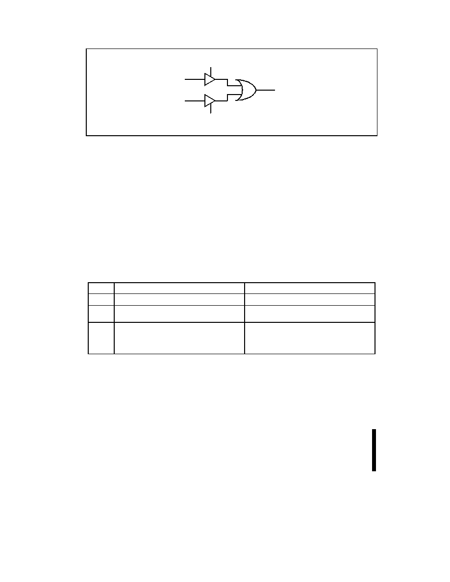
82441FX (PMC) AND 82442FX (DBX)
50
PRELIMINARY
S E F
M E F
E R R C M D [0 ]
E R R C M D [1 ]
SERR#
SERR_GEN
Figure 8. SERR# Generation for Single- or Double-bit Error
When a single or multi-bit error is detected, the offending DRAM row ID is latched in the ERRSTS register in the
PMC. The latched value is held until software explicitly clears the error status flag.
Software Requirements
Initialization. If the ECC feature or parity is enabled, BIOS must take care to properly initialize the memory
before enabling the checking. Software should first ensure PCICMD[SERRE] =0, then enable ECC or parity via
ERRCMD. Next, the entire DRAM array should be written to ensure valid syndrome/parity bits. Finally, the
desired ECC/parity error reporting should be enabled via the ERRCMD and PCICMD registers.
Parity Error Handling. Parity error handling should be via the system's normal NMI routines.
ECC Support Levels. The PMC allows for various levels of ECC support, depending on the specific platform
requirements. The software architecture requirements vary based on the level of support implemented. The
levels and basic software implications are summarized in the table below.
Table 9. ECC Software Levels
Level
Features
Software Requirements
1
- Error Checking/Correction
- Configuration BIOS
2
- Error Checking/Correction.
- Error Scrubbing
- Configuration BIOS.
- SMI Scrubbing Routine
3
- Error Checking/Correction.
- Error Scrubbing.
- System Management (e.g. error logging, error
isolation, memory remapping, etc.)
- Configuration BIOS.
- SMI Scrubbing Routine.
- OS-dependent System management
handler/applet
Level 1
Level 1 defines a minimal support level for ECC handling that would use the system's standard NMI routine.
The configuration BIOS enables SERR# generation only for uncorrectable errors, and disables SERR#
generation for correctable errors. The NMI routine will interpret the uncorrectable error event as a parity
error, and typically reboot the system.

82441FX (PMC) AND 82442FX (DBX)
51
PRELIMINARY
CPU
P M C
P IIX 3
D B X
DBX_ERR#
SERR#
N M I
L1RR_GEN
Figure 9. Level 1 SERR# Generation for ECC and Parity
Level 2
Level 2 adds support for error scrubbing of correctable errors using operating system independent
mechanisms. SMI is the preferred mechanism to implement OS independence. In this case, the SMI
handler would be invoked for both correctable and uncorrectable errors. The DBX_ERR# signal from the
DBX is connected to the PMC as well as the EXT_SMI# input of the PIIX3. Any error signalled via the
DBX_ERR# will trigger a SMI and consequently the SMI handler will be invoked. Note that both
ERRCMD[1:0] bits should be disabled to prevent the generation of SERR# upon receipt of the DBX_ERR#.
For correctable errors, the handler first clears the error flags and then starts a scrub process. The time spent
in an SMI routine should be minimized, since interrupts are disabled and OS services (e.g. real time clocks)
could be adversely affected. To minimize time spent during the SMI handler, the scrub process should be
distributed into small time slices. The handler can setup future SMI events to re-occur based on a hardware
timer (e.g. the "Fast Off" green timer in Intel PCIset standard expansion bridges [PIIX3]) until the memory
scrub has completed.
The following example estimates the worst-case scrub duration for a single correctable error.
Example Assumptions:
∑
128 Mbytes/Row (64Mbit technology) =4M lines at 32 bytes/line
∑
Scrub operation memory bound by linefill + writeback (with medium DRAM timings) = 30 clks/line
∑
SMI scrub time slice budget = 1 msec/SMI
∑
Fast-off SMI interrupt interval = 100 msec/interrupt
With the above assumptions The scrub time is:
∑
the time to scrub one row is 4M lines/row X 30 clks/line X 15ns/clk = 1.8 sec/row.
∑
Thus, spreading the scrub time requires: (1.8 sec/row)/(1msec /SMI) = 1800 SMI events.
∑
The total duration for the scrub SMI events will be 1800 SMI events * 100msec/interrupt = 180 sec.
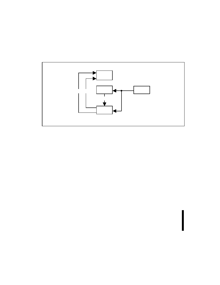
82441FX (PMC) AND 82442FX (DBX)
52
PRELIMINARY
For uncorrectable errors, the SMI handler should first log the error and then pass the error to the system's
normal NMI handler, making it appear as a standard parity error to the software. To pass the NMI event, the
SMI handler will:
∑
Log the MBFRE field and clear the MEF bit
∑
Set ERRCMD[1] to enable SERR# assertion
∑
Write a 1 to MEF bit to cause SERR# assertion
∑
Clear ERRCMD[1] bit to 0 to allow logging of subsequent errors
This will result in a NMI which will be handled after exiting the SMI handler.
CPU
PMC
PIIX3
DBX
DBX_ERR#
SERR#
NMI
SMI
L2RR_GEN
Figure 10. Level 2 SERR# Generation for ECC and Parity
Level 3
Level 3 adds more sophisticated system management functions beyond simple error scrubbing. Typical
functions could include error event logging, error isolation, memory remapping, system diagnostics and user
interface applications. Software to implement Level 3 functions are OS dependent, and beyond the scope of this
document. However, the features used to implement Level 2 functions can also be leveraged in Level 3 systems.
4.3.5.4.
ECC/Parity Test Mode
PMC and DBX provide a software mechanism to test the parity and ECC checking logic. After CRESET# the
DBX ECC/Parity control logic is set in the default mode of operation. To enter the ECC/Parity Test Mode
PMCCFG[EPTE] must be set to 1. This causes the PMC to send a command to the DBX to configure the latter's
ECC/Parity logic for test mode. In the test mode, the DBX signals MDP[7:0] are forced to "0" during writes to
DRAM. During reads, MPD[7:0] are compared against internally generated ECC/Parity Checksum. Errors
generated due to miscompares are reported normally via the DBX_ERR# signal. This mechanism can be used
to test both single-bit and mulitple-bit ECC and parity errors. In case of single-bit errors, a zero pattern can be
written to memory followed by a walking "1" pattern. This should result in the corrected data being returned to
the CPU, (i.e., all 0s). The SEF bit can also be polled to test for single-bit error logging. In case of multiple bit
and parity errors, writing different patterns and reading them back should result in a mulit-bit or parity error which
would be logged in the MEF bit.

82441FX (PMC) AND 82442FX (DBX)
53
PRELIMINARY
4.4.
PCI Bus Arbitration
The PMC's PCI Bus arbiter allows concurrent host and PCI transactions to main memory. The arbiter supports
five PCI masters in addition to the PIIX3 component (Figure 11). REQ[4:0]#/GNT[4:0]# are used by PCI masters.
PHLD#/PHLDA# are the arbitration request/grant signals for the PIIX3 and provide guaranteed access time
capability for ISA masters. The arbiter dynamically allocates to PIIX3 to optimize system latencies for better
Universal Serial Bus (USB) performance.
Multi-Transaction Timer (MTT)
The arbitration mechanism is enhanced with a Multi-Transaction Timer mechanism. The effect of the MTT is to
guarantee a minimum time slice on PCI to an agent that keeps its request asserted. (Note that this mechanism
differs from the MLT operation, that enforces a maximum time slice for an agent.) The MTT algorithm ensures a
fairer bandwidth allocation for PCI devices that generate short burst traffic, or for multi-function devices with
several bus master agents behind one physical PCI interface. This feature improves the PCI bandwidth
allocation to short bursts, an important consideration for example, with typical video capture devices.
Passive Release and Bus Lock
To comply with PCI Specfication, revision 2.1 latency requirements, the PMC supports passive release. The
PMC disables CPU-to-PCI posting during the passive release, except for transactions to the USWC region. The
PMC only supports bus lock mode. The bus lock mode precludes 3rd party locks.
A rbiter
P H L D #
R E Q 0 #
R E Q 1 #
R E Q 2 #
P H L D A #
G N T 0#
G N T 1#
G N T 2#
R E Q 3 #
R E Q 4 #
G N T 3#
G N T 4#
ARBITER
Figure 11. PCI Bus Arbiter
82441FX (PMC) AND 82442FX (DBX)
54
PRELIMINARY
I/O
Bridge
CPU
PCI
Devices
0
1
3
2
4
SYS_ARB
Figure 12. System Arbiter
4.5.
System Clocking and Reset
4.5.1.
HOST FREQUENCY SUPPORT
The Pentium Pro processor uses a clock ratio scheme where the host bus clock frequency is multiplied by a
ratio to produce the processor's core frequency. The PMC supports a host bus frequency ranging up to 66 MHz.
The external synthesizer is responsible for generating the host clock. The Pentium Pro processor samples four
signals LINT[1:0], IGNNE# and A20M# on the active-to-inactive edge of CPURST# to set the ratio.
4.5.2.
CLOCK GENERATION AND DISTRIBUTION
The PMC receives two outputs of a clock synthesizer on the HCLKIN and PCLKIN pins. The DBX also receives
a clock on its HCLKIN pin. The PMC uses the HCLKIN signal to drive the host, memory and private bus and the
PCLKIN bus to drive the PCI interface.
The clock signal requirements for the CPU clock are outlined in the Pentium Pro Bus Input Clock Specification.
The clock skew between two host clock outputs of the synthesizer must be less than 250 ps (at 1.5V). The clock
skew between two PCI clock outputs of the synthesizer must be less than 500 ps (at 1.5V). In addition, the host
clocks should always lead the PCI clocks by a minimum of 1 ns and a maximum of 6 ns. The PMC requires a
45%/55% maximum output duty cycle. A maximum of 200 ps jitter must be maintained on the host clocks going
from cycle to cycle.
4.5.3.
SYSTEM RESET
The PMC contains reset logic for both soft and hard reset. The PMC generates a hard reset at power on. The
PMC can be programmed to generate a hard or a soft reset after power on. The PMC generates a soft reset in
response to a shutdown bus cycle on the CPU bus. External logic is required to combine the PMC soft reset
with the keyboard controller and I/O port 92 soft reset generation. The PMC can also be used to invoke BIST on
the CPU. Figure 13 shows the reset structure for the 440FX PCIset.
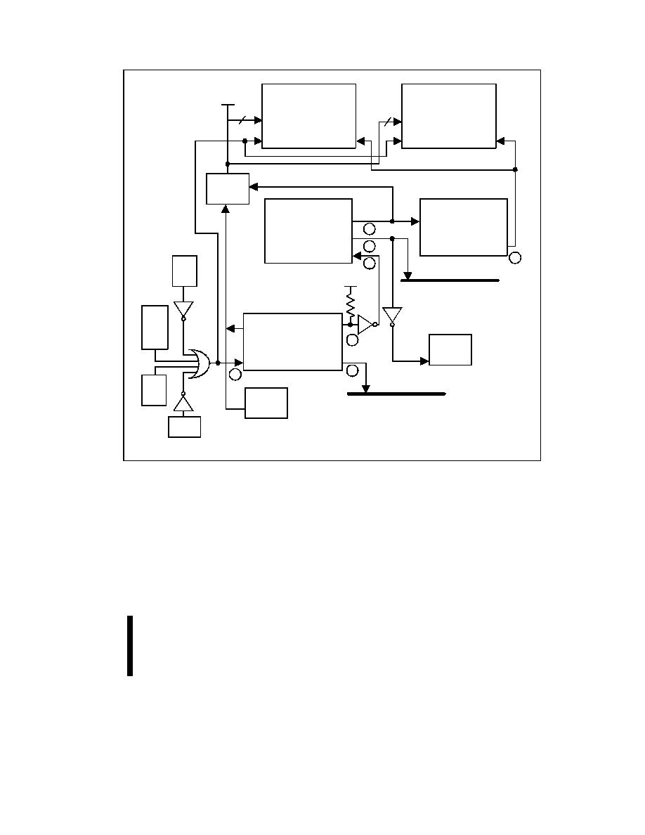
82441FX (PMC) AND 82442FX (DBX)
55
PRELIMINARY
P e n t iu m P ro
P r o ce s s o r
A 2 0 M # , IG N N E # ,
IN TR , N M I#
P W R G D
R E S E T #
P e n tiu m P ro
P ro ce s so r
A 2 0 M # , IG N N E # ,
IN T R , N M I#
P W R G D
R E S E T #
P M C
P W R O K
CR E SE T #
P C IRS T #
DBX
CP U RS T#
CR E S ET #
3.3V
F requ ency
S elec t
Lo gic
PII X3
IG N E E # , IN T R ,
N M I #
PW R O K
C PU RST#
R S TD R V
IO A PIC
R E S E T #
P C I B u s
IS A B u s
4
4
C P U
V C C
82C42
A 2 0 M #
F ro n t
P a n e l
R e s e t
S w itc h
V R M
Power
Supply
ITP
R e se t
1
2
2
2
4
3
3
440FXRES
Figure 13. Reset Structure for 440FX PCIset with PIIX3
4.5.3.1.
Hard Reset
There are two sources of hard reset in the system:
∑
During Power-up, PWROK asserted 1 ms after the system power has stabilized
∑
I/O write to the PMC Turbo/Reset Control Register (configuration offset 93h)
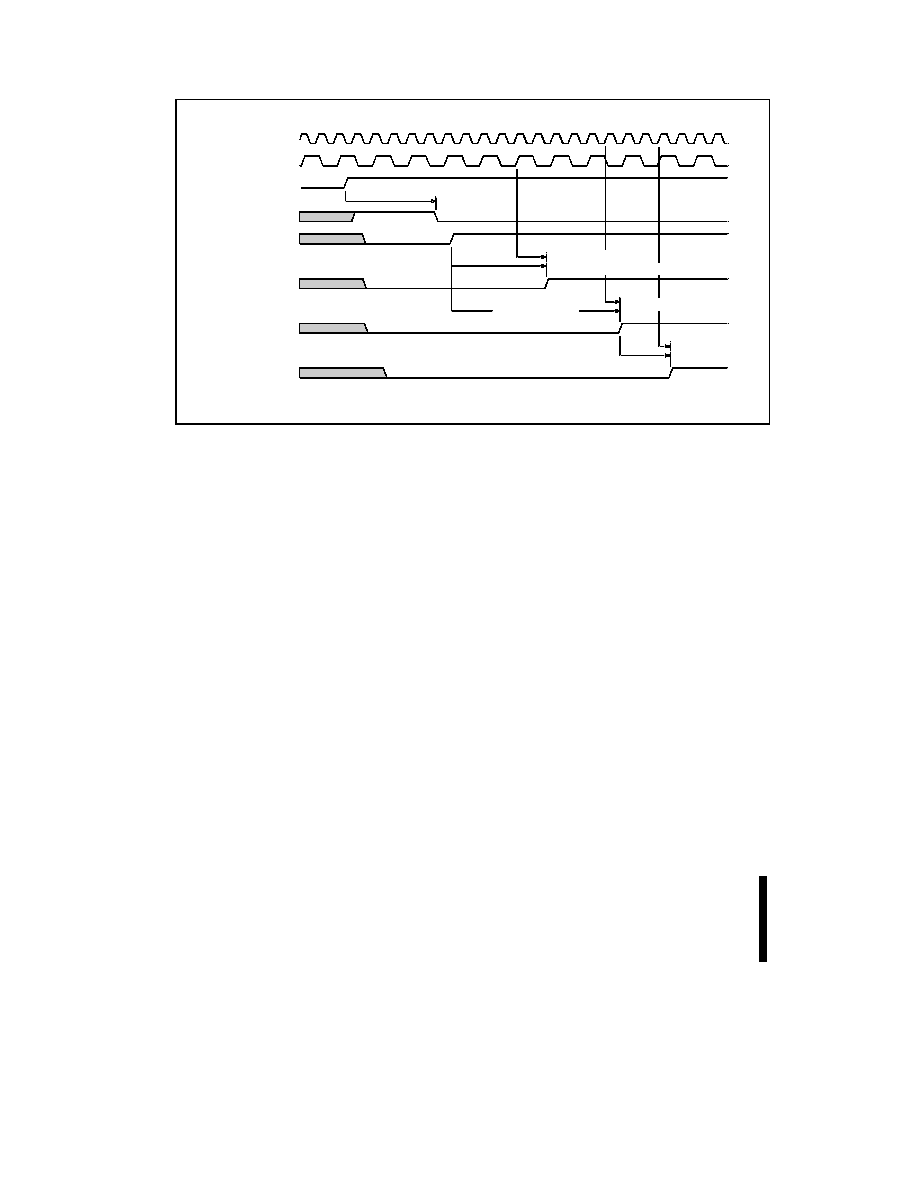
82441FX (PMC) AND 82442FX (DBX)
56
PRELIMINARY
Negation
after 1 msec
tco(PCIRST#)
Negation after 1 msec
Negation after
2 msec
tco(CPURST#)
2 hclks
HCLK
PCLK
PWR_OK (1)
PIIX3 CPURST (2)
PMC PWR_OK (2)
PMC PCIRST# (3)
PMC CRESET# (3)
DBX CPURST# (4)
tco (CRESET#)
RST_DIA
Figure 14. Hard Reset
The PMC generates a hard reset for the system when the PWROK signal is sampled inactive (low). The PMC
generates PCIRST# and CRESET# while the PWROK input is sampled inactive (low). The PMC continues to
assert PCIRST# for 1 msec and CRESET# for 2 msec after sampling PWROK asserted. CRESET# is an input
to the DBX. The DBX drives CPURST# to the CPUs as long as the CRESET# input is sampled active. The DBX
releases CPURST# (external GTL+ pullup will drive it high) 2 host clocks after CRESET# is sampled high by the
DBX. PCIRST# is negated 1 msec after PWROK is asserted and CRESET# is negated 2 msec after PWROK is
negated. CPURST# and CRESET# are released synchronously to the HCLKIN input. PCIRST# is driven
synchronously to the PCLKIN input.
Note that the CPURST# output signal from the PIIX3 should be connected to the PMC's PWROK input signal
through an inverter. This insures that PIIX3 is reset before the first PCI cycle occurs on the PCI bus. Otherwise,
the PWROK signal should be connected to a schmitt trigger buffered version of the power supply
POWER_GOOD signal.
The PMC is the only agent in the system that is allowed to drive PCIRST#. Note that the PCIRST# signal from
the PIIX3 should be left as a no connect.
The PMC can be programmed to generate a hard reset through the Turbo/Reset Control Register (configuration
offset 93h). The PMC asserts CRESET# for a minimum of 2 msec and PCIRST# for 1 msec. The DBX
correspondingly generates the CPURST# to the CPUs. Note that the internal registers of the PMC are also
reset.
NOTE
The PMC should not be used to generate a hard reset in a system designed with PIIX3. Instead use the
PIIX3 to generate the hard reset.
The PMC straps are sampled on the rising edge of PWROK. The DBX receive CRESET# as an input, and reset
the internal DBX state machines. The DBX straps are sampled on the rising edge of CRESET#.
82441FX (PMC) AND 82442FX (DBX)
57
PRELIMINARY
4.5.3.2.
Soft Reset
There are 4 sources of soft reset in the system:
∑
CPU shutdown bus cycle
∑
I/O write to the keyboard controller
∑
I/O write to port 92h
∑
I/O write to the PMC Turbo/Reset Control Register
When the PMC detects a CPU shutdown bus cycle, it terminates the CPU bus cycle with no data response type
as defined in the Pentium Pro processor EBS and then asserts INIT# for a minimum of 4 host clocks. The PMC
can be programmed to generate a soft reset through the Turbo/Reset Control Register (offset 93h). The PMC
asserts INIT# for a minimum of 4 host clocks. The INIT# output of the PMC must be externally gated with the I/O
port 92 (not supported on PIIX3) and keyboard controller soft reset sources as shown in Figure 15.
KBC_RESET#
I/O Port92_RESET#
PMC_INT#
VCC
74F07
CPU_INIT#
RES_SEQ
Figure 15. Reset Sequencing
4.5.3.3.
CPU BIST
The PMC can be programmed to activate BIST mode of the CPU through the Turbo Reset Control register
(offset 93h). The PMC asserts both CRESET# and INIT#. The PMC asserts PCIRST# for 1 msec, CRESET#
for 2 msec and asserts INIT# for 2 msec plus 16 host clocks. The DBX correspondingly asserts CPURST# to
the CPUs. This invokes BIST mode on the CPU.

82441FX (PMC) AND 82442FX (DBX)
58
PRELIMINARY
5.0.
PINOUT AND PACKAGE SPECIFICATIONS
5.1.
PMC Pinout Information
1
2
3
4
5
7
6
8
9
10
1 1
12
1 3
1 4
15
16
1 7
1 8
19
20
2 1
2 2
23
2 4
2 5
26
2 7
2 8
29
30
31
3 2
3 3
34
35
36
3 7
38
39
40
41
42
4 3
44
4 5
46
4 7
48
4 9
50
51
52
G N D
V C C 3
A D 2 9
A D 2 8
A D2 7
A D26
A D 2 5
A D2 4
C / B E 3 #
A D 2 3
A D 2 2
A D21
A D 2 0
A D 1 9
A D 1 8
A D 1 7
A D 1 6
C / B E 2 #
G N D
FRAM E#
I R D Y #
T R D Y #
DE VSEL#
S TO P#
P L O C K
P A R
G N D
VC C3
C / B E 1 #
A D 1 5
A D 1 4
A D 1 3
A D 1 2
A D 1 1
A D 1 0
A D 9
A D 8
C / B E 0 #
A D7
A D 6
A D5
A D 4
A D3
A D 2
A D1
A D0
G N T0#
R E Q 0 -
VC C3
G N D
VC C5
G N D
5
3
5
4
5
5
5
6
5
7
5
8
5
9
6
0
6
1
6
2
6
3
6
4
6
5
6
6
6
7
6
8
6
9
7
0
7
1
7
2
7
3
7
4
7
5
7
6
7
7
7
8
7
9
8
0
8
1
8
2
8
3
8
4
8
5
8
6
8
7
8
8
8
9
9
0
9
1
9
2
9
3
9
4
9
5
9
6
9
7
9
8
9
9
1
0
0
1
0
1
1
0
2
1
0
3
1
0
4
V
C
C
3
G
N
D
G
T
L
_
R
E
F
V
A
D
S
#
R
S
1
#
R
S
2
#
H
I
T
#
B
P
R
I
#
R
S
0
#
G
N
D
D
R
D
Y
#
D
B
S
Y
H
I
T
M
#
H
L
O
C
K
#
H
R
E
Q
3
#
G
N
D
H
R
E
Q
2
#
D
E
F
E
R
#
H
R
E
Q
4
#
H
R
E
Q
1
#
G
N
D
H
R
E
Q
0
#
B
N
R
H
A
6
H
A
4
G
T
L
_
R
E
F
V
H
A
2
3
H
A
9
H
A
5
H
A
8
G
N
D
H
A
1
0
H
A
1
2
H
A
1
4
H
A
1
3
G
N
D
H
A
1
7
H
A
1
6
H
A
1
5
H
A
2
5
H
A
2
1
H
A
2
0
V
C
C
3
V
C
C
3
G
N
D
H
A
1
9
H
T
R
D
Y
#
G
N
D
H
A
3
H
A
7
H
A
1
8
H
A
1
1
105
106
107
108
109
110
111
112
113
114
115
116
117
118
119
120
121
122
12 3
124
125
12 6
127
128
129
130
131
132
133
13 4
135
136
137
138
13 9
140
141
142
143
144
145
146
147
148
149
150
151
152
153
154
155
156
G N D
G N D
H A 2 9
H A 2 8
H A 2 2
H A 2 4
H A 2 7
H A 2 6
H A 3 0
P D9
P D 1 0
P D 1 4
G N D
HC LK IN
FLUS H#
IN IT#
CR ESET#
D D R D Y #
P D 1 5
P D 1 3
P D 1 2
P D 1 1
P D8
V C C 3
P D 7
P C 8
P C 7
P D 6
P D5
P D4
P D3
P D2
P D1
P C6
P C5
P C4
P C3
P D0
P C2
P C 1
P C0
H L A D #
MLAD
MA A0
D B X _ E R R #
G N D
VC C3
G N D
V C C 3
G N D
H A 3 1
MA A1
1
5
7
1
5
8
1
5
9
1
6
0
1
6
1
1
6
2
1
6
3
1
6
4
1
6
5
1
6
6
1
6
7
1
6
8
1
6
9
1
7
0
1
7
1
1
7
2
1
7
3
1
7
4
1
7
5
1
7
6
1
7
7
1
7
8
1
7
9
1
8
0
1
8
1
1
8
2
1
8
3
1
8
4
1
8
5
1
8
6
1
8
7
1
8
8
1
8
9
1
9
0
1
9
1
1
9
2
1
9
3
1
9
4
1
9
5
1
9
6
1
9
7
1
9
8
1
9
9
2
0
0
2
0
1
2
0
2
2
0
3
2
0
4
2
0
5
2
0
6
2
0
7
2
0
8
P M C
C
A
S
1
#
M
A
9
M
A
1
1
G
N
D
M
A
2
M
A
3
M
A
4
M
A
5
M
A
6
M
A
1
0
M
A
7
M
A
8
G
N
D
C
A
S
3
#
C
A
S
7
#
C
A
S
5
#
C
A
S
0
#
C
A
S
4
#
V
C
C
3
C
A
S
2
#
C
A
S
6
#
R
A
S
0
#
R
A
S
1
#
R
A
S
2
#
R
A
S
3
#
R
A
S
4
#
R
A
S
5
#
R
A
S
6
#
\
M
A
B
0
R
A
S
7
#
/
M
A
B
1
W
E
#
G
N
D
P
C
L
K
I
N
P
C
I
R
S
T
#
P
H
L
D
A
#
P
H
O
L
D
#
W
S
C
#
S
E
R
R
#
P
E
R
R
#
R
E
Q
4
#
G
N
T
4
#
R
E
Q
3
#
G
N
T
3
R
E
Q
2
#
G
N
T
2
#
R
E
Q
1
#
G
N
T
1
#
G
N
D
A
D
3
1
A
D
3
0
P
W
R
O
K
G
N
D
V
C
C
3
PMC_PIN
Figure 16. PMC Pinout Diagram

82441FX (PMC) AND 82442FX (DBX)
59
PRELIMINARY
Table 10. PMC Alphabetical
Pin Assignment
Name
Pin#
Type
AD0
46
I/O
AD1
45
I/O
AD2
44
I/O
AD3
43
I/O
AD4
42
I/O
AD5
41
I/O
AD6
40
I/O
AD7
39
I/O
AD8
37
I/O
AD9
36
I/O
AD10
35
I/O
AD11
34
I/O
AD12
33
I/O
AD13
32
I/O
AD14
31
I/O
AD15
30
I/O
AD16
17
I/O
AD17
16
I/O
AD18
15
I/O
AD19
14
I/O
AD20
13
I/O
AD21
12
I/O
AD22
11
I/O
AD23
10
I/O
AD24
8
I/O
AD25
7
I/O
AD26
6
I/O
AD27
5
I/O
AD28
4
I/O
Table 10. PMC Alphabetical
Pin Assignment
Name
Pin#
Type
AD29
3
I/O
AD30
205
I/O
AD31
204
I/O
ADS#
56
I/O
BNR
76
O
BPRI#
75
O
C/BE0#
38
I/O
C/BE1#
29
I/O
C/BE2#
18
I/O
C/BE3#
9
I/O
CAS0#
173
O
CAS1#
171
O
CAS2#
176
O
CAS3#
169
O
CAS4#
174
O
CAS5#
172
O
CAS6#
177
O
CAS7#
170
O
CRESET#
120
O
DBSY
63
I/O
DBX_ERR#
152
I/O
DDRDY#
121
DEFER#
69
O
DEVSEL#
23
I/O
DRDY#
62
I/O
FLUSH#
118
I
FRAME#
20
I/O
GND
1
V
GND
19
V
Table 10. PMC Alphabetical
Pin Assignment
Name
Pin#
Type
GND
27
V
GND
50
V
GND
52
V
GND
54
V
GND
61
V
GND
67
V
GND
73
V
GND
79
V
GND
85
V
GND
91
V
GND
97
V
GND
105
V
GND
106
V
GND
107
V
GND
116
V
GND
153
V
GND
155
V
GND
157
V
GND
168
V
GND
187
V
GND
203
V
GND
207
V
GNT0#
47
O
GNT1#
202
I
GNT2#
200
I
GNT3#
198
I
GNT4#
196
I
GTL_REFV
55
V
GTL_REFV
102
V

82441FX (PMC) AND 82442FX (DBX)
60
PRELIMINARY
Table 10. PMC Alphabetical
Pin Assignment
Name
Pin#
Type
HA3
80
I/O
HA4
78
I/O
HA5
83
I/O
HA6
77
I/O
HA7
82
I/O
HA8
84
I/O
HA9
81
I/O
HA10
86
I/O
HA11
89
I/O
HA12
87
I/O
HA13
90
I/O
HA14
88
I/O
HA15
94
I/O
HA16
93
I/O
HA17
92
I/O
HA18
95
I/O
HA19
98
I/O
HA20
100
I/O
HA21
99
I/O
HA22
109
I/O
HA23
101
I/O
HA24
110
I/O
HA25
96
I/O
HA26
112
I/O
HA27
111
I/O
HA28
108
I/O
HA29
114
I/O
HA30
115
I/O
HA31
113
I/O
Table 10. PMC Alphabetical
Pin Assignment
Name
Pin#
Type
HCLKIN
117
I
HIT#
59
I/O
HITM#
64
I/O
HLAD#
148
O
HLOCK#
65
I
HREQ0#
74
I/O
HREQ1#
72
I/O
HREQ2#
68
I/O
HREQ3#
66
I/O
HREQ4#
71
I/O
HTRDY#
70
I/O
INIT#
119
I
IRDY#
21
I/O
MA2
158
O
MA3
159
O
MA4
160
O
MA5
161
O
MA6
162
O
MA7
164
O
MA8
166
O
MA9
167
O
MA10
163
O
MA11
165
O
MAA0
150
O
MAA1
151
O
MLAD
149
O
PAR
26
I/O
PC0
147
O
PC1
146
O
Table 10. PMC Alphabetical
Pin Assignment
Name
Pin#
Type
PC2
145
O
PC3
144
O
PC4
143
O
PC5
142
O
PC6
141
O
PC7
133
O
PC8
132
O
PCIRST#
189
I
PCLKIN
188
I
PD0
140
O
PD1
139
O
PD2
138
O
PD3
137
O
PD4
136
O
PD5
135
O
PD6
134
O
PD7
131
O
PD8
129
O
PD9
128
O
PD10
127
O
PD11
126
O
PD12
125
O
PD13
124
O
PD14
123
O
PD15
122
O
PERR#
194
I/O
PHLD#
191
I
PHLDA#
190
O
PLOCK
25
I/O

82441FX (PMC) AND 82442FX (DBX)
61
PRELIMINARY
Table 10. PMC Alphabetical
Pin Assignment
Name
Pin#
Type
PWROK
206
I
RAS0#
178
O
RAS1#
179
O
RAS2#
180
O
RAS3#
181
O
RAS4#
182
O
RAS5#
183
O
RAS6#/
MAB0
184
O
RAS7#/
MAB1
185
O
REQ0#
48
I
REQ1#
201
O
REQ2#
199
O
Table 10. PMC Alphabetical
Pin Assignment
Name
Pin#
Type
REQ3#
197
O
REQ4#
195
O
RS0#
60
I/O
RS1#
57
I/O
RS2#
58
I/O
SERR#
193
O
STOP#
24
I/O
TRDY#
22
I/O
VCC3
2
V
VCC3
28
V
VCC3
49
V
VCC3
53
V
VCC3
103
V
Table 10. PMC Alphabetical
Pin Assignment
Name
Pin#
Type
VCC3
104
V
VCC3
130
V
VCC3
154
V
VCC3
156
V
VCC3
175
V
VCC3
208
V
VCC5
51
V
WE#
186
O
WSC#
192
O
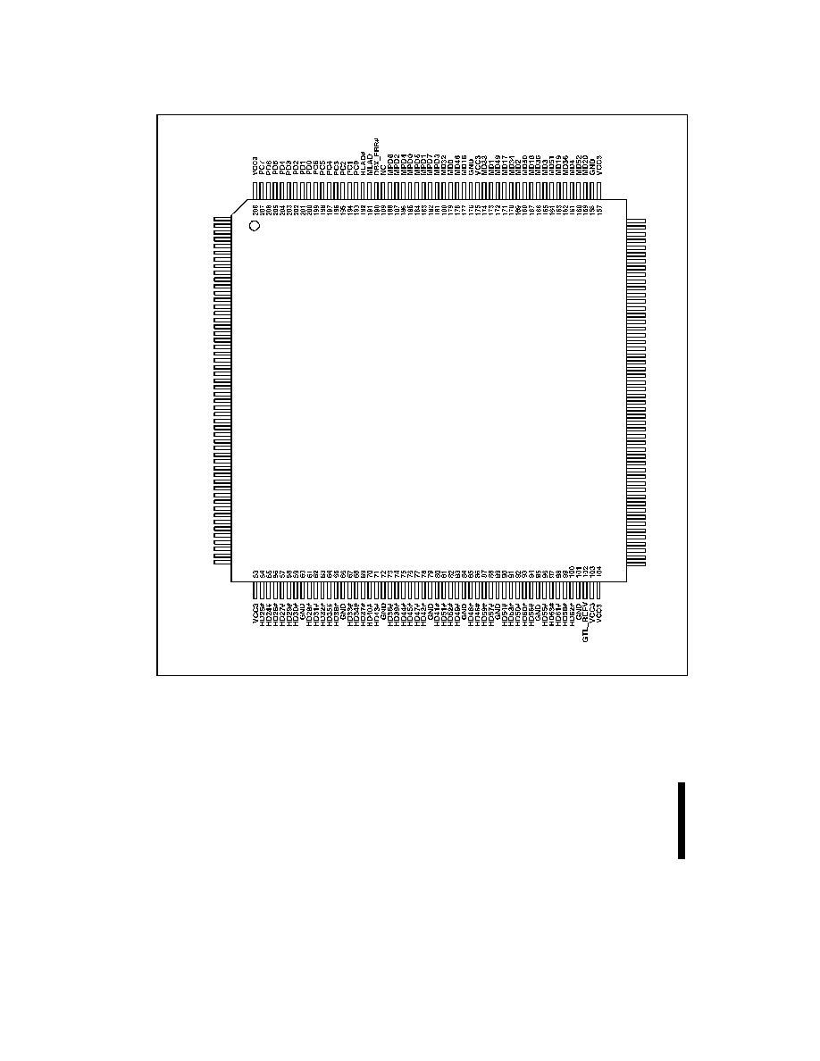
82441FX (PMC) AND 82442FX (DBX)
62
PRELIMINARY
5.2.
DBX Pinout Information
1
2
3
4
5
7
6
8
9
10
11
12
13
14
15
16
17
18
19
20
21
22
23
24
25
26
27
28
29
30
31
32
33
34
35
36
37
38
39
40
41
42
43
44
45
46
47
48
49
50
51
52
GND
VCC3
GND
PC8
PD7
PD8
PD9
PD10
PD11
PD12
PD13
PD14
PD15
DDRDY#
CRESET#
GND
HCLKIN
CPURST#
BREQ0#
GND
HD0#
HD 1#
HD2#
HD3#
HD4#
GND
HD5#
HD6#
HD8#
HD7#
HD9#
GND
HD12#
HD14#
HD15#
HD10#
HD17#
GND
HD11#
HD20#
HD13#
HD18#
HD16#
GND
HD19#
HD21#
HD22#
HD23#
GTL_REFV
GND
GND
GND
105
106
107
108
109
110
111
112
113
114
115
116
117
118
119
120
121
122
123
124
125
126
127
128
129
130
131
132
133
134
135
136
137
138
139
140
141
142
143
144
145
146
147
148
149
150
151
152
153
154
155
156
GND
GND
MD30
MD15
MD47
MD31
MD63
MD14
MD62
MD26
MD43
MD44
MD13
MD45
MD29
MD 61
MD28
MD60
MD12
MD27
MD 59
MD11
MD58
MD10
GND
VCC3
MD 42
MD25
MD57
MD9
MD41
MD24
MD56
MD40
MD23
MD55
MD7
MD8
MD39
MD 22
MD54
MD6
MD38
MD21
MD5
MD37
VCC5
GND
VCC3
GND
MD46
MD53
DBX
DBX_PIN
Figure 17. DBX Pinout Diagram

82441FX (PMC) AND 82442FX (DBX)
63
PRELIMINARY
Table 11. DBX Alphabetical
Pin Assignment
Name
Pin#
Type
BREQ0#
19
O
CPURST#
18
O
CRESET#
15
I
DBX_ERR#
190
I/O
DDRDY#
14
I
GLT_REFV
102
V
GND
1
V
GND
3
V
GND
16
V
GND
20
V
GND
26
V
GND
32
V
GND
38
V
GND
44
V
GND
50
V
GND
51
V
GND
52
V
GND
60
V
GND
66
V
GND
72
V
GND
79
V
GND
84
V
GND
89
V
GND
95
V
GND
101
V
GND
105
V
GND
106
V
GND
107
V
GND
131
V
Table 11. DBX Alphabetical
Pin Assignment
Name
Pin#
Type
GND
155
V
GND
158
V
GND
176
V
GTL_REFV
49
V
HCLKIN
17
I
HD0#
21
I/O
HD1#
22
I/O
HD2#
23
I/O
HD3#
24
I/O
HD4#
25
I/O
HD5#
27
I/O
HD6#
28
I/O
HD7#
30
I/O
HD8#
29
I/O
HD9#
31
I/O
HD10#
36
I/O
HD11#
39
I/O
HD12#
33
I/O
HD13#
41
I/O
HD14#
34
I/O
HD15#
35
I/O
HD16#
43
I/O
HD17#
37
I/O
HD18#
42
I/O
HD19#
45
I/O
HD20#
40
I/O
HD21#
46
I/O
HD22#
47
I/O
HD23#
48
I/O
Table 11. DBX Alphabetical
Pin Assignment
Name
Pin#
Type
HD24#
55
I/O
HD25#
54
I/O
HD26#
56
I/O
HD27#
57
I/O
HD28#
61
I/O
HD29#
58
I/O
HD30#
59
I/O
HD31#
62
I/O
HD32#
63
I/O
HD33#
67
I/O
HD34#
68
I/O
HD35#
64
I/O
HD36#
73
I/O
HD37#
69
I/O
HD38#
65
I/O
HD39#
74
I/O
HD40#
70
I/O
HD41#
80
I/O
HD42#
78
I/O
HD43#
71
I/O
HD44#
75
I/O
HD45#
76
I/O
HD46#
86
I/O
HD47#
77
I/O
HD48#
85
I/O
HD49#
83
I/O
HD50#
92
I/O
HD51#
81
I/O
HD52#
82
I/O

82441FX (PMC) AND 82442FX (DBX)
64
PRELIMINARY
Table 11. DBX Alphabetical
Pin Assignment
Name
Pin#
Type
HD53#
91
I/O
HD54#
90
I/O
HD55#
96
I/O
HD56#
94
I/O
HD57#
88
I/O
HD58#
99
I/O
HD59#
87
I/O
HD60#
93
I/O
HD61#
98
I/O
HD62#
100
I/O
HD63#
97
I/O
HLAD#
192
I
MD0
179
I/O
MD1
173
I/O
MD2
169
I/O
MD3
165
I/O
MD4
161
I/O
MD5
152
I/O
MD6
148
I/O
MD7
144
I/O
MD8
140
I/O
MD9
136
I/O
MD10
130
I/O
MD11
126
I/O
MD12
122
I/O
MD13
116
I/O
MD14
112
I/O
MD15
108
I/O
MD16
177
I/O
Table 11. DBX Alphabetical
Pin Assignment
Name
Pin#
Type
MD17
171
I/O
MD18
167
I/O
MD19
163
I/O
MD20
159
I/O
MD21
150
I/O
MD22
146
I/O
MD23
142
I/O
MD24
138
I/O
MD25
134
I/O
MD26
128
I/O
MD27
124
I/O
MD28
120
I/O
MD29
118
I/O
MD30
114
I/O
MD31
110
I/O
MD32
180
I/O
MD33
174
I/O
MD34
170
I/O
MD35
166
I/O
MD36
162
I/O
MD37
153
I/O
MD38
149
I/O
MD39
145
I/O
MD40
141
I/O
MD41
137
I/O
MD42
133
I/O
MD43
127
I/O
MD44
123
I/O
MD45
117
I/O
Table 11. DBX Alphabetical
Pin Assignment
Name
Pin#
Type
MD46
113
I/O
MD47
109
I/O
MD48
178
I/O
MD49
172
I/O
MD50
168
I/O
MD51
164
I/O
MD52
160
I/O
MD53
151
I/O
MD54
147
I/O
MD55
143
I/O
MD56
139
I/O
MD57
135
I/O
MD58
129
I/O
MD59
125
I/O
MD60
121
I/O
MD61
119
I/O
MD62
115
I/O
MD63
111
I/O
MLAD
191
I
MPD0
185
I/O
MPD1
183
I/O
MPD2
187
I/O
MPD3
181
I/O
MPD4
186
I/O
MPD5
184
I/O
MPD6
188
I/O
MPD7
182
I/O
NC
189
PC0
193
I

82441FX (PMC) AND 82442FX (DBX)
65
PRELIMINARY
Table 11. DBX Alphabetical
Pin Assignment
Name
Pin#
Type
PC1
194
I
PC2
195
I
PC3
196
I
PC4
197
I
PC5
198
I
PC6
199
I
PC7
207
I
PC8
4
I
PD0
200
I
PD1
201
I
PD2
202
I
PD3
203
I
Table 11. DBX Alphabetical
Pin Assignment
Name
Pin#
Type
PD4
204
I
PD5
205
I
PD6
206
I
PD7
5
I
PD8
6
I
PD9
7
I
PD10
8
I
PD11
9
I
PD12
10
I
PD13
11
I
PD14
12
I
PD15
13
I
Table 11. DBX Alphabetical
Pin Assignment
Name
Pin#
Type
VCC3
2
V
VCC3
53
V
VCC3
103
V
VCC3
104
V
VCC3
132
V
VCC3
156
V
VCC3
157
V
VCC3
175
V
VCC3
208
V
VCC5
154
V

82441FX (PMC) AND 82442FX (DBX)
66
PRELIMINARY
5.3.
PMC & DBX Package Specifications
Both PMC and DBX use a 208 pin PQFP package (Figure 18).
A
D
D1
L1
b
Units: mm
1
52
53
104
105
156
157
208
T
A1
Y
* Note* Height Measurements same
as Width Measurements
e1
C
PKG_PIX3
Figure 18. 208 Pin Quad Flat Pack (QFP) Dimensions
Table 12. 208 Pin Quad Flat Pack (QFP) Dimensions
Symbol
Description
Value (mm)
A
Seating Height
4.25 (max)
A1
Stand-off
0.05 (min); 0.40 (max)
b
Lead Width
0.2
±
0.10
C
Lead Thickness
0.15 +0.1/-0.05
D
Package Length and Width, including pins
30.6
±
0.4
D1
Package Length and Width, excluding pins
28
±
0.2
e1
Linear Lead Pitch
0.5
±
0.1
Y
Lead Coplanarity
0.08 (max)
L1
Foot Length
0.5
±
0.2
T
Lead Angle
0o - 10o

82441FX (PMC) AND 82442FX (DBX)
67
PRELIMINARY
6.0.
TESTABILITY
The test modes described below are provided in the 82441FX and 82442FX for Automated Test Equipment
(ATE) board level testing.
PWROK
CRESET#
PMC TEST MODES
PD[15:12]
DBX TEST MODES
PD[5:2]
HRESET
Figure 19. Hard Reset
6.1.
82441FX (PMC) Test Modes
The test mode of the 82441FX is latched at the rising edge of PWROK. The PMC uses PD[15:12] as test mode
inputs. The PMC test modes are selected as shown in Table 13.
Table 13. PMC Test Mode Select
PD15
PD14
PD13
PD12
Mode Selected
0
0
0
0
Normal (Default)
0
0
1
0
NAND Tree
0
0
1
1
All 1s
0
1
0
0
All 0s
1
0
0
1
Tristate
Normal Mode - This is the functional mode of PMC. It is enabled as default via weak 50 K
pulldown devices.
NAND Tree Mode - This allows ATE to test the connectivity of the PMC signal pins. PD[9:8] are outputs of the
NAND tree, PD9 is the end of the NAND tree and PD8 is the midpoint. The procedure for enabling this mode is
as follows:
∑
Initiate HCLK and PCLK. Set PD[15:12]=0011 which is latched on the low to high edge of PWROK. Stop all
clocks.
∑
Put DBX, PIIX3, and IOAPIC in tristate mode.
∑
All inputs are forced high, starting from PD7 (input furthest from PD9), and following the pinout until it ends
with PD10.

82441FX (PMC) AND 82442FX (DBX)
68
PRELIMINARY
∑
Inputs are pulsed low, one at a time starting with PD7. This toggles PD9 each time an input is changed.
The last input in the chain is PD10. NAND Tree order follows the pinout. PWROK, CRESET#, PD9 and
PD8 are not a part of the NAND tree.
131
127
P D [7 ] - N A N D T re e S ta rt In pu t
P D [8 ] - N A N D T re e M i d po int O utp ut
P D [9 ] - N A N D T re e E n d O u tp ut
P D [1 0] - N A N D T re e E nd Inp ut
NAND
Tree
Order
P M C
PMC_NAND
Figure 20. PMC NAND Tree
All 1s Mode - This mode allows all the outputs to be set high (set to 1). Setting PD[15:12]=0011 enables this
mode on the low to high transition of PWROK.
All 0s Mode - This mode allows all the outputs to be set low (set to 0). Setting PD[15:12]=0100 enables this
mode on the low to high transition of PWROK.
Tristate Mode - This mode allows all the outputs to be tristated "High-Z". Setting PD[15:12]=1001 enables this
mode on the low to high transition of PWROK. All GTL+ inputs are turned off.
6.2.
DBX Test Mode
The test mode of the 82442FX is latched at the rising edge of CRESET#. The DBX uses PD[5:2] as test mode
inputs. The DBX test modes are selected as shown in Table 14.
Table 14. DBX Test Mode Select
PD5
PD4
PD3
PD2
Mode Selected
0
0
0
0
Normal (Default)
0
0
1
0
NAND Tree
0
0
1
1
All 1s
0
1
0
0
All 0s
1
0
0
1
Tristate
Normal Mode - This is the functional mode of DBX. It is enabled as default via weak 50 K
pulldown devices.
NAND Tree Mode - This allows ATE to test the connectivity of the DBX signal pins. PD[9:8] are outputs of the
NAND tree; PD9 is the end of the NAND tree and PD8 is the midpoint. The procedure for enabling this mode is
as follows:

82441FX (PMC) AND 82442FX (DBX)
69
PRELIMINARY
∑
Initiate HCLK and PCLK. Set PD[5:2]=0011 which is latched on the low to high edge of CRESET#. Stop all
clocks.
∑
Put PMC, PIIX3, and IOAPIC in tristate mode.
∑
All inputs are forced high, starting from PD7 (input furthest from PD9), and following the pinout until it ends
with PD10.
∑
Inputs are pulsed low, one at a time starting with PD7. This toggles PD9 each time an input is changed. The
last input in the chain is PD10. NAND Tree order follows the pinout. CRESET#, PD9, and PD8 are not a part
of the NAND tree.
N A N D T re e S ta rt In p u t - P D [7 ]
N A N D T re e M i dp o in t O u tp u t - P D [8 ]
N A N D T re e E n d O u tp u t - P D [9 ]
N A N D T re e E n d In p u t - P D [1 0]
NAND
Tree
Order
DBX
DBX_NAND
Figure 21. DBX NAND Tree
All 1s Mode - This mode allows all the outputs to be set high (set to 1). Setting PD[5:2]=0011 enables this mode
on the low to high transition of CRESET#.
All 0s Mode - This mode allows all the outputs to be set low (set to 0). Setting PD[5:2]=0100 enables this mode
on the low to high transition of CRESET#.
Tristate Mode - This mode allows all the outputs to be tristated "High-Z". Setting PD[5:2]=1001 enables this
mode on the low to high transition of CRESET#. All GTL+ inputs are turned off.