 | –≠–ª–µ–∫—Ç—Ä–æ–Ω–Ω—ã–π –∫–æ–º–ø–æ–Ω–µ–Ω—Ç: 440GXAGP | –°–∫–∞—á–∞—Ç—å:  PDF PDF  ZIP ZIP |
Document Outline
- Intel Æ 440GX AGPset Datasheet:
- Intel 82443GX Features
- Contents
- Architectural Overview
- Signal Description
- 2.1 Host Interface Signals
- 2.2 DRAM Interface
- 2.3 PCI Interface (Primary)
- 2.4 Primary PCI Sideband Interface
- 2.5 AGP Interface Signals
- 2.6 Clocks, Reset, and Miscellaneous
- 2.7 Power-Up/Reset Strap Options
- Register Description 3
- 3.1 I/O Mapped Registers
- 3.2 PCI Configuration Space Access
- 3.3 Host-to-PCI Bridge Registers (Device 0)
- 3.4 PCI-to-PCI Bridge Registers (Device 1)
- Functional Description 4
- 4.1 System Address Map
- 4.2 Host Interface
- 4.3 DRAM Interface
- 4.4 PCI Interface
- 4.5 AGP Interface
- 4.6 Data Integrity Support
- 4.7 System Clocking
- 4.8 Power Management
- Pinout and Package Information 5
- 5.1 82443GX Pinout
- 5.2 Package Dimensions
- Testability 6
- 6.1 Test Mode Activation
- 6.2 Tester Powerup Sequence
- 6.3 Test Mode Details
- Intel around the world locations

Intel
Æ
440GX AGPset:
82443GX Host Bridge/Controller
Datasheet
June 1998
Order Number: 290638-001

82443GX Host Bridge
Datasheet
Information in this document is provided in connection with Intel products. No license, express or implied, by estoppel or otherwise, to any intellectual
property rights is granted by this document. Except as provided in Intel's Terms and Conditions of Sale for such products, Intel assumes no liability
whatsoever, and Intel disclaims any express or implied warranty, relating to sale and/or use of Intel products including liability or warranties relating to
fitness for a particular purpose, merchantability, or infringement of any patent, copyright or other intellectual property right. Intel products are not
intended for use in medical, life saving, or life sustaining applications.
Intel may make changes to specifications and product descriptions at any time, without notice.
Contact your local Intel sales office or your distributor to obtain the latest specifications and before placing your product order.
The 82443GX chipset may contain design defects or errors known as errata which may cause the product to deviate from published specifications.
Current characterized errata are available upon request.
I
2
C is a two-wire communications bus/protocol developed by Philips. SMBus is a subset of the I
2
C bus/protocol and was developed by Intel.
Implementations of the I
2
C bus/protocol or the SMBus bus/protocol may require licenses from various entities, including Philips Electronics N.V. and
North American Philips Corporation.
Copies of documents which have an ordering number and are referenced in this document, or other Intel literature may be obtained by:
calling 1-800-548-4725 or
by visiting Intel's website at http://www.intel.com.
Copyright © Intel Corporation, 1997-1998
*Third-party brands and names are the property of their respective owners.

82443GX Host Bridge
Datasheet
iii
Intel 82443GX Features
The Intel
Æ
440GX AGPset is intended for the Pentium
Æ
II processor and Pentium
Æ
II XeonTM
processor platforms. The 82443GX Host Bridge provides a Host-to-PCI bridge, optimized
DRAM controller and data path, and an Accelerated Graphic Port (AGP) interface. AGP is a
high performance, component level interconnect targeted at 3D graphics applications and is
based on a set of performance enhancements to PCI.
The I/O subsystem portion of the Intel
Æ
440GX AGPset platform is based on the 82371EB
(PIIX4E), a highly integrated version of the Intel's PCI-ISA bridge family.
∑
Processor/System bus support
-- Optimized for Pentium
Æ
II and
Pentium
Æ
II XeonTM processors at
100 MHz system bus frequency
-- Supports full symmetric
Multiprocessor (SMP) Protocol for
up to two processors; I/O APIC
related buffer management support
(WSC# signal)
-- In-order transaction and dynamic
deferred transaction support
-- Supports GTL+ and AGTL+ bus
driver technology (gated GTL+
receivers for reduced power)
∑
Integrated DRAM controller
-- 16 MB to 2 GB
-- Supports up to 4 double-sided
DIMMs (8 rows memory)
-- 64-bit data interface with ECC
support (SDRAM only)
-- Unbuffered and Registered
SDRAM (Synchronous) Support
(x-1-1-1 access @ 100 MHz)
-- Enhanced SDRAM Open Page
Architecture Support for 16-, 64-,
128-, and 256-Mbit* DRAM devices
with 2k, 4k and 8k page sizes
∑
PCI bus interface
-- PCI Rev. 2.1, 3.3V and 5V, 33MHz
interface compliant
-- PCI Parity Generation Support
-- Data streaming support from PCI to
DRAM
-- Delayed Transaction support for
PCI-DRAM Reads
-- Supports concurrent CPU, AGP and
PCI transactions to main memory
∑
AGP interface
-- Supports single AGP compliant
device (AGP-66/133 3.3V device)
-- AGP Specification Rev 1.0 compliant
-- AGP-data/transaction flow optimized
arbitration mechanism
-- AGP side-band interface for efficient
request pipelining without
interfering with the data streams
-- AGP-specific data buffering
-- Supports concurrent CPU, AGP and
PCI transactions to main memory
-- AGP high-priority transactions
("expedite") support
∑
Power management functions
-- Stop Clock Grant and Halt special
cycle translation (host to PCI Bus)
-- "Deep Green" Desktop support for
system suspend/resume (i.e., DRAM
and power-on suspend)
-- SDRAM self-refresh power down
support in suspend mode
-- Independent, internal dynamic clock
gating reduces average power
dissipation
-- Static STOP CLOCK support
-- Power-on Suspend mode
-- Suspend to DRAM
-- ACPI compliant power management
∑
Packaging/Voltage
-- 492 Pin BGA
-- 3.3V core & mixed 3.3V & GTL I/O
∑
Supporting I/O Bridge
-- System Management Bus (SMB)
with support for DIMM Serial
Presence Detect (SPD)
-- PCI-ISA Bridge (PIIX4E)
-- Power Management Support
-- 3.3V core and mixed 5V, 3.3V I/O
and interface to the 2.5V CPU signals
via open-drain output buffers
The Intel 82443GX may contain design defects or errors known as errata which may cause the products to deviate from
published specifications. Current characterized errata are available on request.
* Proper operation of the 82443GX AGPset with 256-Mbit SDRAM devices has not yet been verified. Intel's current plans are
to validate this feature in the second half of 1998 when 256-Mbit SDRAM devices are available.
iv
82443GX Host Bridge
Datasheet
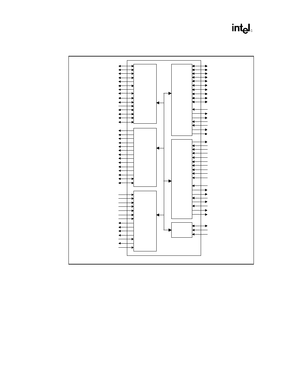
Intel 82443GX Simplified Block Diagram
GX_BLK.VSD
Host
Interface
A[31:3]#
ADS#
BPRI#
BNR#
CPURST#
DBSY#
DEFER#
HD[63:0]#
HIT#
HITM#
HLOCK#
HREQ[4:0]#
HTRDY#
DRDY#
RS[2:0]#
DRAM
Interface
CSA[7:0]#
CSB[7:0]#
DQMA[7:0]
DQMB[5,1]
GCKE
SRAS[B,A]#
FENA
SCAS[B,A]#
MAA[14:0]
MAB[14,13,12#,11#,10,9#:0
#]
WEA#
WEB#
MD[63:0]
MECC[7:0]
HCLKIN
PCLKIN
GTLREF[B:A]
AGPREF
VTT[B:A]
REF5V
PCIRST#
CRESET#
BREQ0#
TESTIN#
GCLKO
GCLKIN
DCLKO
DCLKWR
AD[31:0]
C/BE[3:0]#
FRAME#
TRDY#
IRDY#
DEVSEL#
PAR
SERR#
PLOCK#
STOP#
PHOLD#
PHLDA#
WSC#
PREQ0#
PREQ[4:1]#
PGNT0#
PGNT[4:1]#
GAD[31:0]
GC/BE[3:0]#
GFRAME#
GIRDY#
GTRDY#
GSTOP#
GDEVSEL#
GREQ#
GGNT#
GPAR
PIPE#
SBA[7:0]
RBF#
STOP#
ST[2:0]
ADSTB_A
ADSTB_B
SBSTB
CLKRUN#
SUSTAT#
GXPWROK
PCI Bus
Interface
(PCI #0)
AGP
Interface
Power
Mgnt
Clocks,
Reset,
Test,
and
Misc.

82443GX Host Bridge
Datasheet
v
Contents
1
Architectural Overview ...............................................................................................1-1
2
Signal Description ......................................................................................................2-1
2.1
Host Interface Signals...................................................................................2-1
2.2
DRAM Interface ............................................................................................2-3
2.3
PCI Interface (Primary) .................................................................................2-4
2.4
Primary PCI Sideband Interface ...................................................................2-6
2.5
AGP Interface Signals...................................................................................2-6
2.6
Clocks, Reset, and Miscellaneous ................................................................2-8
2.7
Power-Up/Reset Strap Options.....................................................................2-9
3
Register Description...................................................................................................3-1
3.1
I/O Mapped Registers ...................................................................................3-2
3.1.1
CONFADD--Configuration Address Register..................................3-2
3.1.2
CONFDATA--Configuration Data Register .....................................3-3
3.1.3
PM2_CTL--ACPI Power Control 2 Control Register .......................3-4
3.2
PCI Configuration Space Access..................................................................3-4
3.2.1
Configuration Space Mechanism Overview .....................................3-5
3.2.2
Routing the Configuration Accesses to PCI or AGP ........................3-5
3.2.3
PCI Bus Configuration Mechanism Overview ..................................3-6
3.2.3.1 Type 0 Access ....................................................................3-6
3.2.3.2 Type 1 Access ....................................................................3-6
3.2.4
AGP Bus Configuration Mechanism Overview ................................3-6
3.2.5
Mapping of Configuration Cycles on AGP .......................................3-7
3.3
Host-to-PCI Bridge Registers (Device 0) ......................................................3-8
3.3.1
VID--Vendor Identification Register (Device 0).............................3-10
3.3.2
DID--Device Identification Register (Device 0) .............................3-10
3.3.3
PCICMD--PCI Command Register (Device 0) ..............................3-11
3.3.4
PCISTS--PCI Status Register (Device 0) .....................................3-12
3.3.5
RID--Revision Identification Register (Device 0) ..........................3-13
3.3.6
SUBC--Sub-Class Code Register (Device 0) ...............................3-13
3.3.7
BCC--Base Class Code Register (Device 0) ................................3-13
3.3.8
MLT--Master Latency Timer Register (Device 0)..........................3-14
3.3.9
HDR--Header Type Register (Device 0) .......................................3-14
3.3.10 APBASE--Aperture Base Configuration Register (Device 0)........3-14
3.3.11 SVID--Subsystem Vendor Identification Register (Device 0)........3-15
3.3.12 SID--Subsystem Identification Register (Device 0).......................3-16
3.3.13 CAPPTR--Capabilities Pointer Register (Device 0) ......................3-16
3.3.14 NBXCFG--NBX Configuration Register (Device 0) .......................3-16
3.3.15 DRAMC--DRAM Control Register (Device 0) ...............................3-19
3.3.16 PAM[6:0]--Programmable Attribute Map Registers
(Device 0).......................................................................................3-20
3.3.17 DRB[0:7]--DRAM Row Boundary Registers (Device 0) ................3-22
3.3.18 FDHC--Fixed DRAM Hole Control Register (Device 0) ................3-24
3.3.19 MBSC--Memory Buffer Strength Control Register
(Device 0).......................................................................................3-24
3.3.20 SMRAM--System Management RAM Control Register
(Device 0).......................................................................................3-28

vi
82443GX Host Bridge
Datasheet
3.3.21 ESMRAMC--Extended System Management RAM Control Register
(Device 0) ......................................................................................3-29
3.3.22 RPS--SDRAM Row Page Size Register (Device 0)......................3-30
3.3.23 SDRAMC--SDRAM Control Register (Device 0) ..........................3-30
3.3.24 PGPOL--Paging Policy Register (Device 0) .................................3-32
3.3.25 PMCR--Power Management Control Register (Device 0) ............3-33
3.3.26 SCRR--Suspend CBR Refresh Rate Register (Device 0) ............3-34
3.3.27 EAP--Error Address Pointer Register (Device 0)..........................3-34
3.3.28 ERRCMD--Error Command Register (Device 0) ..........................3-35
3.3.29 ERRSTS--Error Status Register (Device 0)..................................3-36
3.3.30 ACAPID--AGP Capability Identifier Register (Device 0) ...............3-37
3.3.31 AGPSTAT--AGP Status Register (Device 0) ................................3-37
3.3.32 AGPCMD--AGP Command Register (Device 0)...........................3-38
3.3.33 AGPCTRL--AGP Control Register (Device 0) ..............................3-39
3.3.34 APSIZE--Aperture Size Register (Device 0) .................................3-40
3.3.35 ATTBASE--Aperture Translation Table Base Register
(Device 0) ......................................................................................3-40
3.3.36 MBFS--Memory Buffer Frequency Select Register
(Device 0) ......................................................................................3-41
3.3.37 BSPAD--BIOS Scratch Pad Register (Device 0) ..........................3-43
3.3.38 DWTC--DRAM Write Thermal Throttling Control Register
(Device 0) ......................................................................................3-43
3.3.39 DRTC--DRAM Read Thermal Throttling Control Register
(Device 0) ......................................................................................3-44
3.3.40 BUFFC--Buffer Control Register (Device 0) .................................3-45
3.4
PCI-to-PCI Bridge Registers (Device 1) .....................................................3-46
3.4.1
VID1--Vendor Identification Register (Device 1)...........................3-47
3.4.2
DID1--Device Identification Register (Device 1) ...........................3-47
3.4.3
PCICMD1--PCI-to-PCI Command Register (Device 1) ................3-48
3.4.4
PCISTS1--PCI-to-PCI Status Register (Device 1) ........................3-49
3.4.5
RID1--Revision Identification Register (Device 1) ........................3-49
3.4.6
SUBC1--Sub-Class Code Register (Device 1) .............................3-50
3.4.7
BCC1--Base Class Code Register (Device 1) ..............................3-50
3.4.8
MLT1--Master Latency Timer Register (Device 1)........................3-50
3.4.9
HDR1--Header Type Register (Device 1) .....................................3-51
3.4.10 PBUSN--Primary Bus Number Register (Device 1)......................3-51
3.4.11 SBUSN--Secondary Bus Number Register (Device 1) .................3-51
3.4.12 SUBUSN--Subordinate Bus Number Register (Device 1) ............3-52
3.4.13 SMLT--Secondary Master Latency Timer Register
(Device 1) ......................................................................................3-52
3.4.14 IOBASE--I/O Base Address Register (Device 1) ..........................3-52
3.4.15 IOLIMIT--I/O Limit Address Register (Device 1) ...........................3-52
3.4.16 SSTS--Secondary PCI-to-PCI Status Register (Device 1) ...........3-53
3.4.17 MBASE--Memory Base Address Register (Device 1)...................3-54
3.4.18 MLIMIT--Memory Limit Address Register (Device 1)....................3-54
3.4.19 PMBASE--Prefetchable Memory Base Address Register
(Device 1) ......................................................................................3-55
3.4.20 PMLIMIT--Prefetchable Memory Limit Address Register
(Device 1) ......................................................................................3-55
3.4.21 BCTRL--PCI-to-PCI Bridge Control Register (Device 1) ..............3-56

82443GX Host Bridge
Datasheet
vii
4
Functional Description ...............................................................................................4-1
4.1
System Address Map....................................................................................4-1
4.1.1
Memory Address Ranges ................................................................4-2
4.1.1.1 Compatibility Area ...............................................................4-3
4.1.1.2 Extended Memory Area ......................................................4-4
4.1.1.3 AGP Memory Address Range.............................................4-6
4.1.1.4 AGP DRAM Graphics Aperture...........................................4-6
4.1.1.5 System Management Mode (SMM) Memory Range...........4-6
4.1.2
Memory Shadowing .........................................................................4-8
4.1.3
I/O Address Space...........................................................................4-8
4.1.4
AGP I/O Address Mapping...............................................................4-8
4.1.5
Decode Rules and Cross-Bridge Address Mapping ........................4-9
4.1.5.1 PCI Interface Decode Rules ...............................................4-9
4.1.5.2 AGP Interface Decode Rules ..............................................4-9
4.1.5.3 Legacy VGA Ranges ........................................................4-10
4.2
Host Interface..............................................................................................4-10
4.2.1
Host Bus Device Support ...............................................................4-10
4.2.2
Symmetric Multiprocessor (SMP) Protocol Support.......................4-13
4.2.3
In-Order Queue Pipelining .............................................................4-13
4.2.4
Frame Buffer Memory Support (USWC) ........................................4-13
4.3
DRAM Interface ..........................................................................................4-14
4.3.1
DRAM Organization and Configuration..........................................4-14
4.3.1.1 Configuration Mechanism For DIMMS ..............................4-16
4.3.2
DRAM Address Translation and Decoding ....................................4-17
4.3.3
SDRAMC Register Programming ..................................................4-19
4.3.4
SDRAM Paging Policy ...................................................................4-19
4.4
PCI Interface ...............................................................................................4-19
4.5
AGP Interface .............................................................................................4-20
4.6
Data Integrity Support .................................................................................4-20
4.6.1
Data Integrity Mode Selection ........................................................4-20
4.6.1.1 Non-ECC (Default Mode of Operation) .............................4-20
4.6.1.2 EC Mode ...........................................................................4-20
4.6.1.3 ECC Mode ........................................................................4-21
4.6.1.4 ECC Generation and Error Detection/Correction and
Reporting ..........................................................................4-21
4.6.1.5 Optimum ECC Coverage ..................................................4-22
4.6.2
DRAM ECC Error Signaling Mechanism........................................4-22
4.6.3
CPU Bus Integrity ..........................................................................4-22
4.6.4
PCI Bus Integrity ............................................................................4-22
4.7
System Clocking .........................................................................................4-23
4.8
Power Management....................................................................................4-23
4.8.1
Overview ........................................................................................4-23
4.8.2
82443GX Reset .............................................................................4-26
4.8.2.1 CPU Reset ........................................................................4-27
4.8.2.2 CPU Clock Ratio Straps....................................................4-27
4.8.2.3 82443GX Straps ...............................................................4-28
4.8.3
Suspend Resume ..........................................................................4-28
4.8.3.1 Suspend Resume protocols ..............................................4-28
4.8.3.2 Suspend Refresh ..............................................................4-29
4.8.4
Clock Control Functions .................................................................4-29
4.8.5
SMRAM..........................................................................................4-30

viii
82443GX Host Bridge
Datasheet
5
Pinout and Package Information................................................................................5-1
5.1
82443GX Pinout ...........................................................................................5-1
5.2
Package Dimensions ....................................................................................5-8
Figures
1-1
Intel
Æ
440GX AGPset System Block Diagram .............................................1-2
3-1
82443GX PCI Bus Hierarchy ........................................................................3-5
3-2
SDRAM DIMMs and Corresponding DRB Registers ..................................3-23
4-1
Memory System Address Space ..................................................................4-2
4-2
Four-DIMM Configuration with FET switches .............................................4-15
4-3
Typical Intel
Æ
440GX AGPset System Clocking .........................................4-23
4-4
Reset CPURST# in a Desktop System When PCIRST# Asserted .............4-27
4-5
External Glue Logic Drives CPU Clock Ratio Straps ..................................4-28
5-1
82443GX Pinout (Top View≠left side)...........................................................5-2
5-2
82443GX Pinout (Top View≠right side) ........................................................5-3
5-3
82443GX BGA Package Dimensions--Top and Side Views........................5-8
5-4
82443GX BGA Package Dimensions--Bottom Views..................................5-9

82443GX Host Bridge
Datasheet
ix
Tables
2-1
Host Interface Signals...................................................................................2-1
2-2
Host Signals Not supported by the 82443GX ...............................................2-3
2-3
DRAM Interface Signals................................................................................2-3
2-4
Primary PCI Interface Signals.......................................................................2-4
2-5
Primary PCI Sideband Interface Signals.......................................................2-6
2-6
AGP Interface Signals...................................................................................2-6
2-7
Clocks, Reset, and Miscellaneous ................................................................2-8
2-8
Power Management Interface.......................................................................2-9
2-9
Reference Pins .............................................................................................2-9
2-10
Strapping Options .......................................................................................2-10
3-1
82443GX Register Map -- Device 0.............................................................3-8
3-2
Attribute Bit Assignment..............................................................................3-20
3-3
PAM Registers and Associated Memory Segments ...................................3-21
3-4
82443GX Configuration Space--Device 1..................................................3-46
4-1
Memory Segments and their Attributes.........................................................4-3
4-2
SMRAM Decoding ........................................................................................4-7
4-3
SMRAM Range Decode................................................................................4-7
4-4
SMRAM Decode Control...............................................................................4-7
4-5
Host Bus Transactions Supported By 82443GX.........................................4-11
4-6
Host Responses supported by the 82443GX..............................................4-12
4-7
Host Special Cycles with 82443GX ............................................................4-12
4-8
Data Bytes on DIMM Used for Programming DRAM Registers ..................4-16
4-9
Supported Memory Configurations .............................................................4-18
4-10
MA Muxing vs. DRAM Address Split...........................................................4-18
4-11
Programmable SDRAM Timing Parameters ...............................................4-19
4-12
Low Power Mode ........................................................................................4-25
4-13
AGPset Reset .............................................................................................4-26
4-14
Reset Signals..............................................................................................4-26
4-15
Suspend / Resume Events and Activities ...................................................4-28
5-1
82443GX Alphabetical BGA Pin List.............................................................5-4
5-2
82443GX Package Dimensions (492 BGA) ..................................................5-9


82443GX Host Bridge Datasheet
1-1
Architectural Overview
1
The Intel
Æ
440GX AGPset includes the 82443GX Host Bridge and the 82371EB PIIX4E for the
I/O subsystem. The 82443GX functions and capabilities include:
∑
Support for single and dual Pentium
Æ
II processor and Pentium
Æ
II XeonTM processor
configurations
∑
64-bit GTL+ and AGTL+ based System (Host) Bus Interface
∑
32-bit Host address Support
∑
64-bit Main Memory Interface with optimized support for SDRAM at 100 MHz
∑
32-bit Primary PCI Bus Interface (PCI) with integrated PCI arbiter
∑
AGP Interface (AGP) with 133 MHz data transfer capability configurable as a Secondary PCI
Bus
∑
Extensive Data Buffering between all interfaces for high throughput and concurrent operations
∑
"Deep Green" Desktop power management support
Figure 1-1 shows a block diagram of a typical platform based on the Intel
Æ
440GX AGPset. The
82443GX host bus interface supports up to two Pentium II processors or two Pentium II XeonTM
processors at 100 MHz bus frequency. The physical interface design is based on the GTL+
specification optimized for the desktop. The 82443GX provides an optimized 64-bit DRAM
interface. This interface is implemented as a 3.3V-only interface that supports only 3V DRAM
technology. Two copies of the MA, and CS# signals drive a maximum of two DIMMs each;
providing unbuffered high performance at 100 MHz. The 82443GX provides interface to PCI
operating at 33 MHz. This interface implementation is compliant with PCI Rev 2.1 Specification.
The 82443GX AGP interface implementation is based on Rev 1.0 of the AGP Specification. The
AGP interface supports 133 MHz data transfer rates.
The 82443GX is designed to support the PIIX4E I/O bridge. PIIX4E is a highly integrated
multifunctional component supporting the following functions and capabilities:
∑
PCI Rev 2.1 compliant PCI-ISA Bridge with support for both 3.3V and 5V 33 MHz PCI
operations
∑
Deep Green Desktop Power Management Support
∑
Enhanced DMA controller and Interrupt Controller and Timer functions
∑
Integrated IDE controller with Ultra DMA/33 support
∑
USB host interface with support for 2 USB ports
∑
System Management Bus (SMB) with support for DIMM Serial PD
∑
Support for an external I/O APIC component

Architectural Overview
1-2
82443GX Host Bridge Datasheet
Host Interface
The Pentium
Æ
II processor and Pentium
Æ
II XeonTM processor support a second level cache via a
cache bus interface. All control for the L2 cache is handled by the processor. The 82443GX
provides bus control signals and address paths for transfers between the processors system bus
(host bus), PCI bus, AGP and main memory. The 82443GX supports a 4-deep in-order queue (i.e.,
supports pipelining of up to 4 outstanding transaction requests on the host bus). Due to the system
concurrency requirements, along with support for pipelining of address requests from the host bus,
the 82443GX supports request queuing for all three interfaces (Host, AGP and PCI).
Host-initiated I/O cycles are decoded to PCI, AGP or PCI configuration space. Host-initiated
memory cycles are decoded to PCI, AGP (prefetchable or non-prefetchable memory space) or
DRAM (including AGP aperture memory). For memory cycles (host, PCI or AGP initiated) that
target the AGP aperture space in DRAM, the 82443GX translates the address using the AGP
address translation table. Other host cycles forwarded to AGP are defined by the AGP address map.
PCI and AGP initiated cycles that target the AGP graphics aperture are also translated using the
AGP aperture translation table. AGP-initiated cycles that target the AGP graphics aperture mapped
in main memory do not require a snoop cycle on the host bus, since the coherency of data for that
particular memory range will be maintained by the software.
Figure 1-1. Intel
Æ
440GX AGPset System Block Diagram
sys_blk.vsd
TV
Video BIOS
System Bus
82443GX
Host Bridge
Main
Memory
Pentium
Æ
II or
Pentium
Æ
II
XeonTM Processor
3.3V SDRAM
Support
2X AGP Bus
Graphics
Device
Display
ISA Bus
ISA Slots
System BIOS
System MGMT (SM) Bus
2 IDE Ports
(Ultra DMA/33)
2 USB
Ports
USB
USB
IO
APIC
82371EB
(PIIX4E)
(PCI-to-ISA
Bridge)
Primary PCI Bus
(PCI Bus #0)
PCI Slots
Encoder
Graphics
Local Memory
Video
- DVD
- Camera
- VCR
- VMI
- Video Capture
100 MHz
Pentium
Æ
II or
Pentium
Æ
II
XeonTM Processor

82443GX Host Bridge Datasheet
1-3
Architectural Overview
DRAM Interface
The 82443GX integrates a DRAM controller that supports a 64-bit main memory interface. The
DRAM controller supports the following features:
∑
DRAM type: Synchronous DRAM (SDRAM) controller optimized for dual/quad-bank
SDRAM organization on a row by row basis
∑
Memory Size: 16 MB to 2 GB with eight memory rows
∑
Addressing Type: Asymmetrical addressing
∑
Memory Modules supported: Single and double-sided 3.3V DIMMs
∑
DRAM device technology: 16 Mbit, 64 Mbit, 128 Mbit, and 256 Mbit
1
∑
DRAM Speed: 100 MHz synchronous memory (SDRAM).
The Intel
Æ
440GX AGPset also provides DIMM plug-and-play support via Serial Presence Detect
(SPD) mechanism using the SMBus interface. The 82443GX provides optional data integrity
features including ECC in the memory array. During reads from DRAM, the 82443GX provides
error checking and correction of the data. The 82443GX supports multiple-bit error detection and
single-bit error correction when ECC mode is enabled and single/multi-bit error detection when
correction is disabled. During writes to the DRAM, the 82443GX generates ECC for the data on a
QWord basis. Partial QWord writes require a read-modify-write cycle when ECC is enabled.
AGP Interface
The 82443GX AGP implementation is compatible with the following:
∑
The Accelerated Graphics Port Specification, Rev 1.0
∑
Accelerated Graphics Port Memory Performance Specification, Rev 1.0 (4/12/96)
The 82443GX supports only a synchronous AGP interface coupling to the 82443GX core
frequency. The AGP interface can reach a theoretical ~500 MByte/sec transfer rate (i.e., using
133 MHz AGP compliant devices).
PCI Interface
The 82443GX PCI interface is 3.3V (5V tolerant), 33 MHz Rev. 2.1 compliant and supports up to
five external PCI bus masters in addition to the I/O bridge (PIIX4/PIIX4E). The PCI-to-DRAM
interface can reach over 100 MByte/sec transfer rate for streaming reads and over 120 MBytes/sec
for streaming writes.
System Clocking
The 82443GX operates the host interface, SDRAM, and core at 100 MHz only; PCI at
33 MHz; and AGP at 66/133 MHz.
I/O APIC
I/O APIC is used to support dual processors as well as enhanced interrupt processing in the single
processor environment. The 82443GX supports an external status output signal that can be used to
control synchronization of interrupts in configurations that use PIIX4E with stand-alone I/O APIC
component.
1.
Proper operation of the 82443GX AGPset with 256-Mbit SDRAM devices has not yet been verified. Intel's current plans are to validate this feature
in the second half of 1998 when 256-Mbit SDRAM devices are available.

82443GX Host Bridge Datasheet
2-1
Signal Description
S i g n a l D e s c r i p t i o n
2
This chapter provides a detailed description of 82443GX signals. The signals are arranged in
functional groups according to their associated interface.
The "#" symbol at the end of a signal name indicates that the active, or asserted state occurs when
the signal is at a low voltage level. When "#" is not present after the signal name the signal is
asserted when at the high voltage level.
The following notations are used to describe the signal type:
I
Input pin
O
Output pin
OD
Open Drain Output pin. This pin requires a pullup to the VCC of the processor core
I/OD
Input / Open Drain Output pin. This pin requires a pullup to the VCC of the processor
core
I/O
Bi-directional Input/Output pin
The signal description also includes the type of buffer used for the particular signal:
GTL+ Open Drain GTL+ interface signal. Refer to the GTL+ I/O Specification for complete
details
PCI
PCI bus interface signals. These signals are compliant with the PCI 3.3V and 5.0V
Signaling Environment DC and AC Specifications
AGP
AGP interface signals. These signals are compatible with AGP 3.3V Signaling
Environment DC and AC Specifications
CMOS The CMOS buffers are Low Voltage TTL compatible signals. These are 3.3V only.
2.1
Host Interface Signals
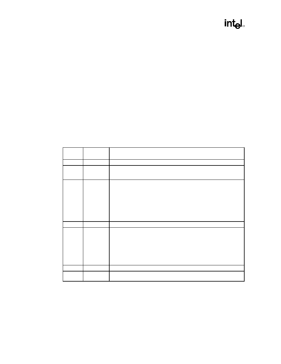
Table 2-1. Host Interface Signals (Sheet 1 of 2)
Name
Type
Description
CPURST#
O
GTL+
CPU Reset. The CPURST# pin is an output from the 82443GX. The 82443GX
generates this signal based on the PCIRST# input (from PIIX4E) and also the
SUSTAT# pin in mobile mode. The CPURST# allows the CPUs to begin execution in
a known state.
A[31:3]#
I/O
GTL+
Address Bus: A[31:3]# connect to the CPU address bus. During CPU cycles, the
A[31:3]# are inputs.
HD[63:0]#
I/O
GTL+
Host Data: These signals are connected to the CPU data bus. Note that the data
signals are inverted on the CPU bus.
Signal Description
2-2
82443GX Host Bridge Datasheet
NOTE:
1. All of the signals in the host interface are described in the CPU External Bus Specification. The preceding
table highlights 82443GX specific uses of these signals.
ADS#
I/O
GTL+
Address Strobe: The CPU bus owner asserts ADS# to indicate the first of two
cycles of a request phase.
BNR#
I/O
GTL+
Block Next Request: Used to block the current request bus owner from issuing a
new request. This signal is used to dynamically control the CPU bus pipeline depth.
BPRI#
O
GTL+
Priority Agent Bus Request: The 82443GX is the only Priority Agent on the CPU
bus. It asserts this signal to obtain the ownership of the address bus. This signal has
priority over symmetric bus requests and will cause the current symmetric owner to
stop issuing new transactions unless the HLOCK# signal was asserted.
BREQ0#
O
GTL+
Symmetric Agent Bus Request: Asserted by the 82443GX when CPURST# is
asserted to configure the symmetric bus agents. BREQ0# is negated 2 host clocks
after CPURST# is negated.
DBSY#
I/O
GTL+
Data Bus Busy: Used by the data bus owner to hold the data bus for transfers
requiring more than one cycle.
DEFER#
O
GTL+
Defer: The 82443GX generates a deferred response as defined by the rules of the
82443GX's dynamic defer policy. The 82443GX also uses the DEFER# signal to
indicate a CPU retry response.
DRDY#
I/O
GTL+
Data Ready: Asserted for each cycle that data is transferred.
HIT#
I/O
GTL+
Hit: Indicates that a caching agent holds an unmodified version of the requested line.
Also driven in conjunction with HITM# by the target to extend the snoop window.
HITM#
I/O
GTL+
Hit Modified: Indicates that a caching agent holds a modified version of the
requested line and that this agent assumes responsibility for providing the line. Also
driven in conjunction with HIT# to extend the snoop window.
HLOCK#
I
GTL+
Host Lock: All CPU bus cycles sampled with the assertion of HLOCK# and ADS#,
until the negation of HLOCK# must be atomic, i.e. no PCI or AGP snoopable access
to DRAM is allowed when HLOCK# is asserted by the CPU.
HREQ[4:0]#
I/O
GTL+
Request Command: Asserted during both clocks of request phase. In the first clock,
the signals define the transaction type to a level of detail that is sufficient to begin a
snoop request. In the second clock, the signals carry additional information to define
the complete transaction type. The transactions supported by the 82443GX Host
Bridge are defined in the Host Interface section of this document.
HTRDY#
I/O
GTL+
Host Target Ready: Indicates that the target of the CPU transaction is able to enter
the data transfer phase.
RS[2:0]#
I/O
GTL+
Response Signals: Indicates type of response according to the following the table:
RS[2:0]
Response type
000
Idle state
001
Retry response
010 Deferred
response
011
Reserved (not driven by 82443GX)
100
Hard Failure (not driven by 82443GX)
101
No data response
110
Implicit Writeback
111
Normal data response
Table 2-1. Host Interface Signals (Sheet 2 of 2)
Name
Type
Description

82443GX Host Bridge Datasheet
2-3
Signal Description
Table 2-2 lists the CPU bus interface signals which are NOT supported by the Intel
Æ
440GX
AGPset.
2.2
DRAM Interface
Table 2-2. Host Signals Not supported by the 82443GX
Signal
Function
Not Supported By 82443GX
A[35:32]#
Address
Extended addressing (over 4 GB)
AERR#
Address Parity Error
Parity protection on address bus
AP[1:0]#
Address Parity
Parity protection on address bus
BINIT#
Bus Initialization
Checking for bus protocol violation and protocol recovery mechanism
DEP[7:0]#
Data Bus ECC/Parity
Enhanced data bus integrity
IERR#
Internal Error
Direct internal error observation via IERR# pin
INIT#
Soft Reset
Implemented by PIIX4E, BIST supported by external logic.
BERR#
Bus Error
Unrecoverable error without a bus protocol violation
RP#
Request Parity
Parity protection on ADS# and PREQ[4:0]#
RSP#
Response Parity
Signal
Parity protection on RS[2:0]#
BP[3:2]#
BreakPoint
Breakpoint status
BPM[1:0]#
BreakPoint Monitor
Breakpoint and performance monitor
Table 2-3. DRAM Interface Signals (Sheet 1 of 2)
Name
Type
Description
CSA[7:0]#
/CSB[7:0]#
O
CMOS
Chip Select (SDRAM): These pins perform the function of selecting the
particular SDRAM components during the active state.
Note that there are 2 copies of CS# per physical memory row to improve the
loading.
DQMA[7:0]
O
CMOS
Input/Output Data Mask A-side: These pins control A half of the memory array
and act as synchronized output enables during read cycles and as a byte enables
during write cycles.
DQMB[1,5]
O
CMOS
Input/Output Data Mask B-side (SDRAM): The same function as the
corresponding signals for the A side (DQMAx). These signals are used to reduce
the loading in an ECC configuration.
GCKE
O
CMOS
Global CKE: Global CKE is used in a 4 DIMM configuration requiring power
down mode for the SDRAM. External logic must be used to implement this
function.
SRAS[B,A]#
O
CMOS
SDRAM Row Address Strobe: The SRAS[B,A]# signals are multiple copies of
the same logical SRASx signal (for loading purposes) used to generate SDRAM
command encoded on SRASx/SCASx/WE signals.
FENA
O
CMOS
FET Enable (FENA): FENA is used to select the proper MD path through the
FET switches in a 4 DIMM configuration.
SCAS[B,A]#
O
CMOS
SDRAM Column Address Strobe: The SCAS[B,A]# signals are multiple copies
of the same logical SCASx signal (for loading purposes) used to generate
SDRAM command encoded on SRASx/SCASx/WE signals.
Signal Description
2-4
82443GX Host Bridge Datasheet
2.3
PCI Interface (Primary)
MAA[14:0]
MAB[12:11]#
MAB[14,13,10]
MAB[9:0]#
O
CMOS
Memory Address(SDRAM): MAA[14:0] and MAB[14,13,12#,11#,10,9#:0#] are
used to provide the multiplexed row and column address to DRAM. There are two
sets of MA signals which drive a max. of 2 DIMMs each. MAB[12:11,9:0]# are
inverted copies of MAA[12:11,9:0]. MAA[14,13,10] and MAB[14,13,10] are
identical copies. Each MAA/MAB[14:0] line has a programmable buffer strength to
optimize for different signal loading conditions.
WEA#
WEB#
O
CMOS
Write Enable Signa: WE# is asserted during writes to DRAM. The WE# lines
have a programmable buffer strength to optimize for different signal loading
conditions.
MD[63:0]
I/O
CMOS
Memory Data: These signals are used to interface to the DRAM data bus.
MECC[7:0]
I/O
CMOS
Memory ECC Data: These signals carry Memory ECC data during access to
DRAM.
Table 2-4. Primary PCI Interface Signals (Sheet 1 of 2)
Name
Type
Description
AD[31:0]
I/O
PCI
PCI Address/Data: These signals are connected to the PCI address/data bus.
Address is driven by the 82443GX with FRAME# assertion, data is driven or received
in the following clocks. When the 82443GX acts as a target on the PCI Bus, the
AD[31:0] signals are inputs and contain the address during the first clock of FRAME#
assertion and input data (writes) or output data (reads) on subsequent clocks.
DEVSEL#
I/O
PCI
Device Select: Device select, when asserted, indicates that a PCI target device has
decoded its address as the target of the current access. The 82443GX asserts
DEVSEL# based on the DRAM address range or
AGP address range
being accessed
by a PCI initiator. As an input it indicates whether any device on the bus has been
selected.
FRAME#
I/O
PCI
Frame: FRAME# is an output when the 82443GX acts as an initiator on the PCI Bus.
FRAME# is asserted by the 82443GX to indicate the beginning and duration of an
access. The 82443GX asserts FRAME# to indicate a bus transaction is beginning.
While FRAME# is asserted, data transfers continue. When FRAME# is negated, the
transaction is in the final data phase. FRAME# is an input when the 82443GX acts as
a PCI target. As a PCI target, the 82443GX latches the C/BE[3:0]# and the AD[31:0]
signals on the first clock edge on which it samples FRAME# active.
IRDY#
I/O
PCI
Initiator Ready: IRDY# is an output when 82443GX acts as a PCI initiator and an
input when the 82443GX acts as a PCI target. The assertion of IRDY# indicates the
current PCI Bus initiator's ability to complete the current data phase of the
transaction.
Table 2-3. DRAM Interface Signals (Sheet 2 of 2)
Name
Type
Description

82443GX Host Bridge Datasheet
2-5
Signal Description
NOTE:
1. All PCI interface signals conform to the PCI Rev 2.1 specification.
C/BE[3:0]#
I/O
PCI
Command/Byte Enable: PCI Bus Command and Byte Enable signals are
multiplexed on the same pins. During the address phase of a transaction, C/BE[3:0]#
define the bus command. During the data phase C/BE[3:0]# are used as byte
enables. The byte enables determine which byte lanes carry meaningful data. PCI
Bus command encoding and types are listed below.
C/BE[3:0]#
Command Type
0000
Interrupt Acknowledge
0001
Special Cycle
0010
I/O Read
0011
I/O Write
0100
Reserved
0101
Reserved
0110
Memory Read
0111
Memory Write
1000
Reserved
1001
Reserved
1010
Configuration Read
1011
Configuration Write
1100
Memory Read Multiple
1101
Reserved (Dual Address Cycle)
1110
Memory Read Line
1111
Memory Write and Invalidate
PAR
I/O
PCI
Parity: PAR is driven by the 82443GX when it acts as a PCI initiator during address
and data phases for a write cycle, and during the address phase for a read cycle. PAR
is driven by the 82443GX when it acts as a PCI target during each data phase of a
PCI memory read cycle. Even parity is generated across AD[31:0] and C/BE[3:0]#.
PLOCK#
I/O
PCI
Lock: PLOCK# indicates an exclusive bus operation and may require multiple
transactions to complete. When PLOCK# is asserted, non-exclusive transactions may
proceed. The 82443GX supports lock for CPU initiated cycles only. PCI initiated
locked cycles are not supported.
TRDY#
I/O
PCI
Target Ready: TRDY# is an input when the 82443GX acts as a PCI initiator and an
output when the 82443GX acts as a PCI target. The assertion of TRDY# indicates the
target agent's ability to complete the current data phase of the transaction.
SERR#
I/O
PCI
System Error: The 82443GX asserts this signal to indicate an error condition. The
SERR# assertion by the 82443GX is enabled globally via SERRE bit of the PCICMD
register. SERR# is asserted under the following conditions:
In an ECC configuration, the 82443GX asserts SERR#, for single bit (correctable)
ECC errors or multiple bit (non-correctable) ECC errors if SERR# signaling is enabled
via the ERRCMD control register. Any ECC errors received during initialization should
be ignored.
∑
The 82443GX asserts SERR# for one clock when it detects a target abort during
82443GX initiated PCI cycle.
∑
The 82443GX can also assert SERR# when a PCI parity error occurs during the
address or data phase.
∑
The 82443GX can assert SERR# when it detects a PCI address or data parity
error on AGP.
∑
The 82443GX can assert SERR# upon detection of access to an invalid entry in
the Graphics Aperture Translation Table.
∑
The 82443GX can assert SERR# upon detecting an invalid AGP master access
outside of AGP aperture and outside of main DRAM range (i.e. in the 640k - 1M
range or above TOM).
∑
The 82443GX can assert SERR# upon detecting an invalid AGP master access
outside of AGP aperture.
∑
The 82443GX asserts SERR# for one clock when it detects a target abort during
82443GX initiated AGP cycle.
STOP#
I/O
PCI
Stop: STOP# is an input when the 82443GX acts as a PCI initiator and an output
when the 82443GX acts as a PCI target. STOP# is used for disconnect, retry, and
abort sequences on the PCI Bus.
Table 2-4. Primary PCI Interface Signals (Sheet 2 of 2)
Name
Type
Description
Signal Description
2-6
82443GX Host Bridge Datasheet
2.4
Primary PCI Sideband Interface
2.5
AGP Interface Signals
There are 17 new signals added to the normal PCI group of signals that together constitute the AGP
interface. The sections below describe their operation and use, and are organized in five groups:
∑
AGP Addressing Signals
∑
AGP Flow Control Signals
∑
AGP Status Signals
∑
AGP Clocking Signals - Strobes
∑
PCI Signals
Table 2-5. Primary PCI Sideband Interface Signals
Name
Type
Description
PHOLD#
I
PCI
PCI Hold: This signal comes from the PIIX4E. It is the PIIX4E request for PCI bus
ownership. The 82443GX will flush and disable the CPU-to-PCI write buffers before
granting the PIIX4E the PCI bus via PHLDA#. This prevents bus deadlock between
PCI and ISA.
PHLDA#
O
PCI
PCI Hold Acknowledge: This signal is driven by the 82443GX to grant PCI bus
ownership to the PIIX4E after CPU-PCI post buffers have been flushed and disabled.
WSC#
O
CMOS
Write Snoop Complete. This signal is asserted active to indicate that all that the
snoop activity on the CPU bus on the behalf of the last PCI-DRAM write transaction is
complete and that is safe to send the APIC interrupt message.
PREQ[4:0]#
I
PCI
PCI Bus Request: PREQ[4:0]# are the PCI bus request signals used as inputs by the
internal PCI arbiter.
PGNT[4:0]#
O
PCI
PCI Grant: PGNT[4:0]# are the PCI bus grant output signals generated by the internal
PCI arbiter.
Table 2-6. AGP Interface Signals (Sheet 1 of 3)
Name
Type
Description
AGP Sideband Addressing Signals
1
PIPE#
I
AGP
Pipelined Read:
This signal is asserted by the current master to indicate a full width
address is to be queued by the target. The master queues one request each rising
clock edge while PIPE# is asserted. When PIPE# is deasserted no new requests are
queued across the AD bus. PIPE# is a sustained tri-state signal from
masters
(graphics controller)
and is an input to the 82443GX. Note that initial AGP designs
may not use PIPE#.
SBA[7:0]
I
AGP
Sideband Address: This bus
provides an additional bus to pass address and
command to the 82443GX from the AGP master. Note that, when sideband
addressing is disabled, these signals are isolated (no external/internal pull-ups are
required).
AGP Flow Control Signals
RBF#
I
AGP
Read Buffer Full.
This signal indicates if the master is ready to accept previously
requested low priority read data. When RBF# is asserted the 82443GX is not allowed
to return low priority read data to the AGP master on the first block. RBF# is only
sampled at the beginning of a cycle.
If the AGP master is always ready to accept return read data then it is not required to
implement this signal.
82443GX Host Bridge Datasheet
2-7
Signal Description
AGP Status Signals
ST[2:0]
O
AGP
Status
Bus: This bus provides information from the arbiter to a AGP Master on what
it may do. ST[2:0] only have meaning to the master when its GGNT# is asserted.
When GGNT# is deasserted these signals have no meaning and must be ignored.
000 Indicates that previously requested low priority read data is being returned to
the master.
001 Indicates that previously requested high priority read data is being returned to
the master.
010 Indicates that the master is to provide low priority write data for a previously
queued write command.
011 Indicates that the master is to provide high priority write data for a previously
queued write command.
100 Reserved
101 Reserved
110 Reserved
111 Indicates that the master has been given permission to start a bus transaction.
The master may queue AGP requests by asserting PIPE# or start a PCI
transaction by asserting FRAME#. ST[2:0] are always an output from the
82443GX and an input to the master.
AGP Clocking Signals - Strobes
ADSTB_A
I/O
AGP
AD Bus Strobe A: This signal provides timing for double clocked data on the AD bus.
The agent that is providing data drives this signal. This signal requires an 8.2K ohm
external pull-up resistor.
ADSTB_B
I/O
AGP
AD Bus Strobe B: This signal is an additional copy of the AD_STBA signal. This
signal requires an 8.2K ohm external pull-up resistor.
SBSTB
I
AGP
Sideband Strobe: THis signal provides timing for a side-band bus. This signal
requires an 8.2K ohm external pull-up resistor.
AGP FRAME# Protocol SIgnals (similar to PCI)
2
GFRAME#
I/O
AGP
Graphics Frame: Same as PCI. Not used by AGP. GFRAME# remains deasserted
by its own pull up resistor.
GIRDY#
I/O
AGP
Graphics Initiator Ready: New meaning. GIRDY# indicates the AGP compliant
master is ready to provide
all
write data for the current transaction. Once IRDY# is
asserted for a write operation, the master is not allowed to insert wait states. The
assertion of IRDY# for reads indicates that the master is ready to transfer to a
subsequent block (32 bytes) of read data. The master is
never
allowed to insert wait
states during the initial data transfer (32 bytes) of a read transaction. However, it may
insert wait states after each 32 byte block is transferred.
(There is no GFRAME# -- GIRDY# relationship for AGP transactions.)
GTRDY#
I/O
AGP
Graphics Target Ready: New meaning. GTRDY# indicates the AGP compliant
target is ready to provide read data for the entire transaction (when the transfer size is
less than or equal to 32 bytes) or is ready to transfer the initial or subsequent block
(32 bytes) of data when the transfer size is greater than 32 bytes. The target is
allowed to insert wait states after each block (32 bytes) is transferred on both read
and write transactions.
GSTOP#
I/O
AGP
Graphics Stop: Same as PCI. Not used by AGP.
GDEVSEL#
I/O
AGP
Graphics Device Select: Same as PCI. Not used by AGP.
GREQ#
I
AGP
Graphics Request: Same as PCI. (Used to request access to the bus to initiate a
PCI or AGP request.)
Table 2-6. AGP Interface Signals (Sheet 2 of 3)
Name
Type
Description
Signal Description
2-8
82443GX Host Bridge Datasheet
NOTE:
1.
AGP Sideband Addressing Signals.
The above table contains two mechanisms to queue requests by
the AGP master. Note that the master can only use one mechanism. When PIPE# is used to queue
addresses the master is not allowed to queue addresses using the SBA bus. For example, during
configuration time, if the master indicates that it can use either mechanism, the configuration software will
indicate which mechanism the master will use. Once this choice has been made, the master will continue to
use the mechanism selected until the master is reset (and reprogrammed) to use the other mode. This
change of modes is not a dynamic mechanism but rather a static decision when the device is first being
configured after reset.
2. PCI signals are redefined when used in AGP transactions carried using AGP protocol extension. For
transactions on the AGP interface carried using PCI protocol these signals completely preserve PCI
semantics. The exact role of all PCI signals during AGP transactions is in Table 2-6.
3. The LOCK# signal is not supported on the AGP interface (even for PCI operations).
4. PCI signals described in Table 2-4 behave according to PCI 2.1 specifications when used to perform PCI
transactions on the AGP Interface.
2.6
Clocks, Reset, and Miscellaneous
GGNT#
O
AGP
Graphics Grant: Same meaning as PCI but additional information is provided on
ST[2:0]. The additional information indicates that the selected master is the recipient
of previously requested read data (high or normal priority), it is to provide write data
(high or normal priority), for a previously queued write command or has been given
permission to start a bus transaction (AGP or PCI).
GAD[31:0]
I/O
AGP
Graphics Address/Data: Same as PCI.
GC/BE[3:0]#
I/O
AGP
Graphics Command/Byte Enables: Slightly different meaning. Provides command
information (different commands than PCI) when requests are being queued when
using PIPE#. Provide valid byte information during AGP write transactions and are
not used during the return of read data.
GPAR
I/O
AGP
Graphics Parity: Same as PCI. Not used on AGP transactions, but used during PCI
transactions as defined by the PCI specification.
Table 2-6. AGP Interface Signals (Sheet 3 of 3)
Name
Type
Description
Table 2-7. Clocks, Reset, and Miscellaneous (Sheet 1 of 2)
Name
Type
Description
HCLKIN
I
CMOS
Host Clock In: This pin receives a buffered host clock. This clock is used by all of the
82443GX logic that is in the Host clock domain.
When SUSTAT# is active, there is an internal 100K ohm pull down on this signal.
PCLKIN
I
CMOS
PCI Clock In: This is a buffered PCI clock reference that is synchronously derived by
an external clock synthesizer component from the host clock. This clock is used by all
of the 82443GX logic that is in the PCI clock domain.
When SUSTAT# is active, there is an internal 100K ohm pull down on this signal.
DCLKO
O
CMOS
SDRAM Clock Out: 100 MHz SDRAM clock reference. It feeds an external buffer
clock device that produces multiple copies for the DIMMs.
DCLKWR
I
CMOS
SDRAM Write Clock: Feedback reference from the external SDRAM clock buffer.
PCIRST#
I
CMOS
PCI Reset: When asserted, this signal will reset the 82443GX logic. All PCI output
and bi-directional signals will also tri-state compliant to PCI Rev 2.0 and 2.1
specifications.
When SUSTAT# is active, there is an internal 100K ohm pull down on this signal.
GCLKIN
I
CMOS
AGP Clock In: The GCLKIN input is a feedback reference from the GCLKOUT signal.
82443GX Host Bridge Datasheet
2-9
Signal Description
2.7
Power-Up/Reset Strap Options
Table 2-10 is the list of all power-up options that are loaded into the 82443GX during cold reset.
The 82443GX is required to float all the signals connected to straps during cold reset and keep
them floated for a minimum of 4 host clocks after the end of cold reset sequence. Cold reset
sequence is performed when the 82443GX power is applied.
Note:
All signals used to select power-up strap options are connected to either internal pull-down or pull-
up resistors of minimum 50K ohms (maximum is 150K). That selects a default mode on the signal
during reset. To enable different modes, external pull ups or pull downs (the opposite of the internal
GCLKO
O
CMOS
AGP Clock Out: The frequency is 66 MHz. The GCLKOUT output is used to feed
both the reference input pin on the 82443GX and the AGP compliant device.
CRESET#
O
CMOS
Delayed CPU Reset: CRESET# is a delayed copy of CPURST#. This signal is used
to control the multiplexer for the CPU strap signals. CRESET# is delayed from
CPURST# by two host clocks.
Note: This pin requires an external pull-up resistor. If not used, no pull up is required.
TESTIN#
I
CMOS
Test Input: This pin is used for manufacturing, and board level test purposes.
Note: This pin has an internal 50K ohm pull-up.
Table 2-8. Power Management Interface
Name
Type
Description
CLKRUN#
I/OD
CMOS
Primary PCI Clock Run: The 82443GX requests the central resource (PIIX4E) to
start or maintain the PCI clock by the assertion of CLKRUN#. The 82443GX tristates
CLKRUN# upon deassertion of PCIRST# (since CLK is running upon deassertion of
reset). If connected to PIIX4E an external 2.7K Ohm pull-up is required for Desktop,
Mobile requires (8.2k≠10K) pull-up. Otherwise, a 100 Ohm pull down is required.
SUSTAT#
I
CMOS
Suspend Status (from PIIX): SUSTAT# signals the system suspend state transition
from the PIIX4E. It is used to isolate the suspend voltage well and enter/exit DRAM
self-refresh mode. During POS/STR SUSTAT# is active.
GXPWROK
I
CMOS
GX Power OK: GXPWROK input must be connected to the PWROK signal that
indicates valid power is applied to the 82443GX.
Table 2-9. Reference Pins
Name
Description
GTLREF[B:A]
GTL Buffer voltage reference input
VTT[B:A]
GTL Threshold voltage for early clamps
VCC
Power pin @ 3.3V
VSS
Ground
REF5V
PCI 5V reference voltage (for 5V tolerant buffers)
AGPREF
External Input Reference
Table 2-7. Clocks, Reset, and Miscellaneous (Sheet 2 of 2)
Name
Type
Description
Signal Description
2-10
82443GX Host Bridge Datasheet
resistor) of approximately 10K ohm can be connected to particular signals. These pull up or pull
down resistors should be connected to the 3.3V power supply.
During normal operation of the 82443GX, including while it is in suspend mode, the paths from
GND or Vcc to internal strapping resistors are disabled to effectively disable the resistors. In these
cases, the MAB# lines are driven by the 82443GX to a valid voltage levels.
Note:
Note that when resuming from suspend, even while PCIRST# is active, the MAB# lines remain
driven by the 82443GX and the strapping latches maintain the value stored during the cold reset.
This first column in Table 2-10 lists the signal that is sampled to obtain the strapping option. The
second column shows which register the strapping option is loaded into. The third column is a
description of what functionality the strapping selects.
The GTL+ signals are connected to the VTT through the normal pull-ups. CPU bus straps
controlled by the 82443GX (e.g. A7# and A15#), are driven active at least six clocks prior to the
active-to-inactive edge of CPURST# and driven inactive four clocks after the active-to-inactive
edge of the CPURST#.
NOTE:
1. Proper strapping must be used to define logical values for these signals. Default value "0", or "1" provided by
the internal pull-up or pull-down resistor can be overridden by the external pull-up, or pull-down resistor.
Table 2-10. Strapping Options
Signal
Register
Name[bit]
Description
MAB13#
Reserved.
MAB12#
NBXCFG[13]
MAB12# is strapped to 1 for a host bus frequency of 100 MHz. Strapping
MAB12# to 0 is a reserved condition. An internal pull-down provides a default
setting of 0.
MAB11#
NBXCFG[2]
In-Order Queue Depth Enable: If MAB11# is strapped to 0 during the rising
edge of PCIRST#, then the 82442GX will drive A7# low during the CPURST#
deassertion. This forces the CPU bus to be configured for non-pipelined
operation.
If MAB11 is strapped to 1 (default), then the 82443GX does not drive the A7# low
during reset, and A7# is sampled in default non-driven state (i.e. pulled-up as far
as GTL+ termination is concerned) then the maximum allowable queue depth by
the CPU bus protocol is selected (i.e., 8).
Note that internal pull-up is used to provide pipelined bus mode as a default.
MAB10
--
Reserved.
MAB9#
PMCR[1]
AGP Disable: When strapped to a 1, the AGP interface is disabled, all AGP
signals are tri-stated and isolated. When strapped to a 0 (default), the AGP
interface is enabled.
When MMCONFIG is strapped active, we require that AGP_DISABLE is also
strapped active. When MMCONFIG is strapped inactive, AGP_DISABLE can be
strapped active or inactive but IDSEL_REDIRECT (bit 16 in NBXCFG register)
must never be activated.
This signal has an internal pull-down resistor.
MAB[8:6]
--
Reserved.
A[7]#
none
In-order Queue Depth Status: The value on A[7]# sampled at the rising edge of
CPURST# reflects if the IOQD is set to 1 or maximum allowable by the CPU bus.

82443GX Host Bridge Datasheet
3-1
Register Description
R e g i s t e r D e s c r i p t i o n
3
The 82443GX contains two sets of software accessible registers, accessed via the Host CPU I/O
address space:
1. Control registers that are I/O mapped into the CPU I/O space. These registers control access to
PCI and AGP configuration space.
2. Internal configuration registers residing within the 82443GX, partitioned into two logical
device register sets ("logical" since they reside within a single physical device). The first
register set is dedicated to Host-to-PCI Bridge functionality. This set (device 0) controls PCI
interface operations, DRAM configuration, and other chip-set operating parameters and
optional features. The second register set (device 1) is dedicated to Host-to-AGP Bridge
functions (controls AGP interface configurations and operating parameters).
The following nomenclature is used for register access attributes.
The 82443GX supports PCI configuration space access using the mechanism denoted as
Configuration Mechanism #1 in the PCI specification.
The 82443GX internal registers (both I/O Mapped and Configuration registers) are accessible by
the Host CPU. The registers can be accessed as Byte, Word (16-bit), or DWord (32-bit) quantities,
with the exception of CONFADD which can only be accessed as a Dword. All multi-byte numeric
fields use "little-endian" ordering (i.e., lower addresses contain the least significant parts of the
field).
Some of the 82443GX registers described in this section contain reserved bits. These bits are
labeled "Reserved". Software must deal correctly with fields that are reserved. On reads, software
must use appropriate masks to extract the defined bits and not rely on reserved bits being any
particular value. On writes, software must ensure that the values of reserved bit positions are
preserved. That is, the values of reserved bit positions must first be read, merged with the new
values for other bit positions and then written back.
Note:
Software does not need to perform read, merge, write operation for the configuration address
register.
In addition to reserved bits within a register, the 82443GX contains address locations in the
configuration space of the Host-to-PCI Bridge entity that are marked either "Reserved" or "Intel
Reserved". The 82443GX responds to accesses to "Reserved" address locations by completing the
host cycle. When a "Reserved" register location is read, a zero value is returned. ("Reserved"
registers can be 8-, 16-, or 32-bit in size). Writes to "Reserved" registers have no effect on the
RO
Read Only. If a register is read only, writes to this register have no effect.
R/W
Read/Write. A register with this attribute can be read and written
R/WC
Read/Write Clear. A register bit with this attribute can be read and written.
However, a write of a 1 clears (sets to 0) the corresponding bit and a write of a 0 has
no effect.
R/WO
Read/Write Once. A register bit with this attribute can be written to only once after
power up. After the first write, the bit becomes read only.
R/WL
Read/Write/Lock. This register includes a lock bit. Once the lock bit has been set to
1, the register becomes read only.

Register Description
3-2
82443GX Host Bridge Datasheet
82443GX. Registers that are marked as "Intel Reserved" must not be modified by system software.
Writes to "Intel Reserved" registers may cause system failure. Reads to "Intel Reserved" registers
may return a non-zero value. Software should not write to reserved configuration locations in the
device-specific region (above address offset 3Fh)
Upon reset, the 82443GX sets its internal configuration registers to predetermined default states.
However, there are a few exceptions to this rule.
1. When a reset occurs during the POS/STR state, several configuration bits are not reset to their
default state. These bits are noted in the following register description.
2. Some register values at reset are determined by external strapping options.
The default state represents the minimum functionality feature set required to successfully bring up
the system. Hence, it does not represent the optimal system configuration. It is the responsibility of
the system initialization software (usually BIOS) to properly determine the DRAM configurations,
operating parameters and optional system features that are applicable, and to program the
82443GX registers accordingly.
3.1
I/O Mapped Registers
The 82443GX contains three registers that reside in the CPU I/O address space - the Configuration
Address (CONFADD) Register, the Configuration Data (CONFDATA) Register, and the Power
Management Control Register. The Configuration Address Register enables/disables the
configuration space and determines what portion of configuration space is visible through the
Configuration Data window.
3.1.1
CONFADD--Configuration Address Register
I/O Address:
0CF8h Accessed as a Dword
Default Value:
00000000h
Access:
Read/Write
Size:
32 bits
CONFADD is a 32 bit register accessed only when referenced as a Dword. A Byte or Word
reference will "pass through" the Configuration Address Register onto the PCI bus as an I/O cycle.
The CONFADD register contains the Bus Number, Device Number, Function Number, and
Register Number for which a subsequent configuration access is intended.

82443GX Host Bridge Datasheet
3-3
Register Description
3.1.2
CONFDATA--Configuration Data Register
I/O Address:
0CFCh
Default Value:
00000000h
Access:
Read/Write
Size:
32 bits
CONFDATA is a 32 bit read/write window into configuration space. The portion of configuration
space that is referenced by CONFDATA is determined by the contents of CONFADD.
Bit
Descriptions
31
Configuration Enable (CFGE). When this bit is set to 1 accesses to PCI configuration space are
enabled. If this bit is reset to 0 accesses to PCI configuration space are disabled.
30:24
Reserved.
23:16
Bus Number. When the Bus Number is programmed to 00h the target of the Configuration Cycle
is either the 82443GX or the PCI Bus that is directly connected to the 82443GX, depending on the
Device Number field. A type 0 Configuration Cycle is generated on PCI if the Bus Number is
programmed to 00h and the 82443GX is not the target. If the Bus Number is non-zero a type 1
configuration cycle is generated on PCI or AGP with the Bus Number mapped to AD[23:16] during
the address phase.
15:11
Device Number. This field selects one agent on the PCI bus selected by the Bus Number. During
a Type 1 Configuration cycle this field is mapped to AD[15:11]. During a Type 0 Configuration
Cycle this field is decoded and one bit among AD[31:11] is driven to a 1. The 82443GX is always
Device Number 0 for the Host-to-PCI bridge entity and Device Number 1 for the Host- AGP entity.
Therefore, the 82443GX internally references the AD11 and AD12 pins as corresponding IDSELs
for the respective devices during PCI configuration cycles. NOTE: The AD11 and AD12 must not
be connected to any other PCI bus device as IDSEL signals.
10:8
Function Number. This field is mapped to AD[10:8] during PCIx configuration cycles. This allows
the configuration registers of a particular function in a multi-function device to be accessed. The
82443GX only responds to configuration cycles with a function number of 000b; all other function
number values attempting access to the 82443GX (Device Number = 0 and 1, Bus Number = 0)
will generate a master abort.
7:2
Register Number. This field selects one register within a particular Bus, Device, and Function as
specified by the other fields in the Configuration Address Register. This field is mapped to AD[7:2]
during PCI configuration cycles.
1:0
Reserved.
Bit
Descriptions
31:0
Configuration Data Window (CDW). If bit 31 of CONFADD is 1 any I/O reference that falls in the
CONFDATA I/O space will be mapped to configuration space using the contents of CONFADD.

Register Description
3-4
82443GX Host Bridge Datasheet
3.1.3
PM2_CTL--ACPI Power Control 2 Control Register
I/O Address:
0022h
Default Value:
00h
Access:
Read/Write
Size:
8 bits
This register is used to disable both the PCI and AGP arbiters in the 82443GX to prevent any
external bus masters from acquiring the PCI or AGP bus. Any currently running PCI cycles will
terminate properly.
Accesses to this register are controlled by the Power Management Control Register (Offset 7Ah).
When bit 6 of the PMCR is set to `1', the ACPI Register at I/O location 0022h is enabled. When bit
6 is set to `0', I/O accesses to location 0022h are forwarded to PCI or AGP (if within programmable
IO range).
3.2
PCI Configuration Space Access
The 82443GX implementation manifests two PCI devices within a single physical component
body:
∑
Device 0 = Host-to-PCI Bridge = PCI bus #0 interface, Main Memory Controller, Graphics
Aperture controller, 82443GX specific AGP control registers.
∑
Device 1 = Host-to-AGP interface = "Virtual" PCI-to-PCI Bridge, including AGP address
space mapping, normal PCI interface, and associated AGP sideband signal control.
Corresponding configuration registers for both devices are mapped as devices residing on PCI (bus
0). Configuration register layout and functionality for the Device #0 should be inspected carefully,
as new features added to the 82443GX initiated a reasonable level of change relative to other
proliferation's of the Pentium
Æ
Pro processor AGPsets (i.e. 440FX, 440LX). Configuration
registers of the 82443GX Device #1 are based on the normal configuration space template of a
PCI-to-PCI Bridge as described in the PCI to PCI Bridge Architecture Specification.
Figure 3-1 shows the PCI bus hierarchy for the 82443GX. In the PCI bus hierarchy, the primary
PCI bus is the highest level bus in the hierarchy and is PCI bus #0. The PCI-to-PCI bridge function
provides access to the AGP/PCI bus 0. This bus is below the primary bus in the PCI bus hierarchy
and is represented as PCI Bus #1.
Bit
Description
7:1
Reserved
0
Primary PCI and AGP Arbiter Request Disable (ARB_DIS). When this bit is set to 1, the
82443GX will not respond to any PCI REQ# signals, AGP requests, or PHOLD# from PIIX4E going
active until this bit is set back to 0. Only External AGP and PCI requests are masked from the
arbiters. If the PIIX is in passive release mode, masking will not occur until an active release is seen
via PHLDA# assertion. This prevents possible deadlock.
ARB_DIS has no effect on AGP side band signals or AGP data transfer requests.
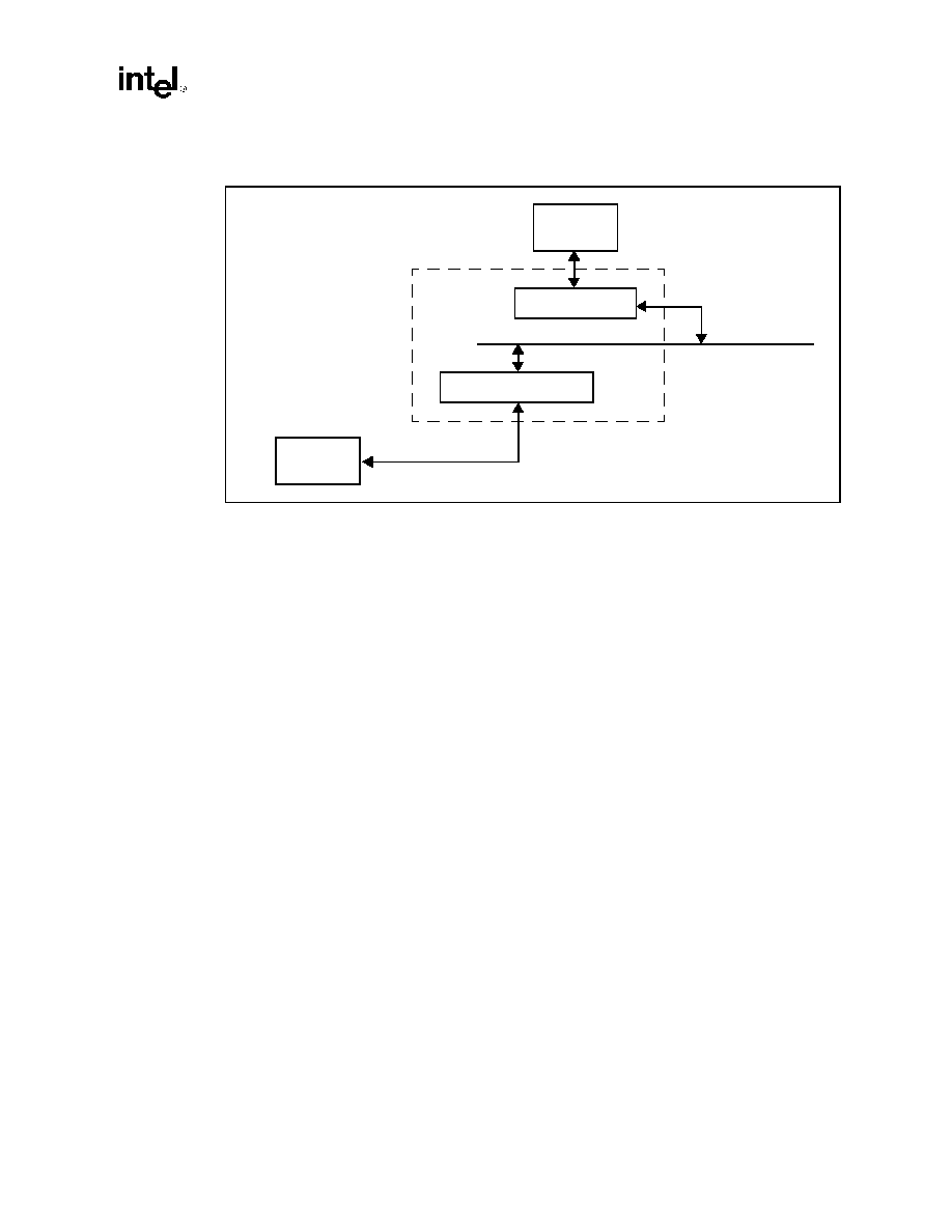
82443GX Host Bridge Datasheet
3-5
Register Description
3.2.1
Configuration Space Mechanism Overview
The 82443GX supports two bus interfaces: PCI (referenced as Primary PCI) and AGP (referenced
as AGP). The AGP interface is treated as a second PCI bus from the configuration point of view.
The following sections describe the configuration space mapping mechanism associated with both
buses.
Note:
The configuration space for device #1 is controlled by the AGP_DIS bit in the PMCR register.
When the AGP_DIS bit (PMCR[1]) is set to 0, the configuration space for device #1 is enabled, and
the registers for device #1 are accessible through the configuration mechanism defined below.
When the AGP_DIS bit (PMCR[1]) is set to 1, the configuration space for device #1 is disabled.
All configuration cycles (reads and writes) to device #1 of bus 0 will cause the master abort status
bit for device #0/ bus 0 to be set. Configuration read cycles will return data of all 1's. Configuration
write cycles will have no effect on the registers.
3.2.2
Routing the Configuration Accesses to PCI or AGP
Routing of configuration accesses to AGP is controlled via PCI-to-PCI bridge normal mechanism
using information contained within the PRIMARY BUS NUMBER, the SECONDARY BUS
NUMBER, and the SUBORDINATE BUS NUMBER registers of the Host-to-AGP internal
"virtual" PCI-to-PCI bridge device. Detailed description of the mechanism for translating CPU I/O
bus cycles to configuration cycles on one of the two buses is described below.
To distinguish between PCI configuration cycles targeting the two logical device register sets
supported in the 82443GX, this document refers to the Host-to-PCI bridge PCI interface as PCI and
the Host- AGP PCI interface as AGP.
Figure 3-1. 82443GX PCI Bus Hierarchy
CPU
Host-to-PCI Bridge
Virtual Host-to-PCI Bridge
AGP Device
PCI Bus #0
82443GX
Host Bridge
PCI Bus #1 ≠ AGP

Register Description
3-6
82443GX Host Bridge Datasheet
3.2.3
PCI Bus Configuration Mechanism Overview
The PCI Bus defines a slot based "configuration space" that allows each device to contain up to 8
functions with each function containing up to 256 8-bit configuration registers. The PCI
specification defines two bus cycles to access the PCI configuration space: Configuration Read
and Configuration Write. Memory and I/O spaces are supported directly by the CPU.
Configuration space is supported by a mapping mechanism implemented within the chip-set. The
PCI specification defines two mechanisms to access configuration space, Mechanism #1 and
Mechanism #2. The 82443GX supports only Mechanism #1.
The configuration access mechanism makes use of the CONFADD Register and CONFDATA
Register. To reference a configuration register a Dword I/O write cycle is used to place a value into
CONFADD that specifies the PCI bus, the device on that bus, the function within the device, and a
specific configuration register of the device function being accessed. CONFADD[31] must be 1 to
enable a configuration cycle. CONFDATA then becomes a window into the four bytes of
configuration space specified by the contents of CONFADD. Any read or write to CONFDATA will
result in the Host Bridge translating CONFADD into a PCI configuration cycle.
3.2.3.1
Type 0 Access
If the Bus Number field of CONFADD is 0, a Type 0 Configuration cycle is performed on PCI (i.e.
bus #0). CONFADD[10:2] is mapped directly to AD[10:2]. The Device Number field of
CONFADD is decoded onto AD[31:11]. The Host-to-PCI Bridge entity within the 82443GX is
accessed as Device #0 on the PCI bus segment. The Host- /AGP Bridge entity within the 82443GX
is accessed as Device #1 on the PCI bus segment. To access Device #2, the 82443GX will assert
AD13, for Device #3 will assert AD14, and so forth up to Device #20 for which will assert AD31.
Only one AD line is asserted at a time. All device numbers higher than 20 cause a type 0
configuration access with no IDSEL asserted, which will result in a Master Abort.
3.2.3.2
Type 1 Access
If the Bus Number field of CONFADD is non-zero, then a Type 1 Configuration cycle is performed
on PCI bus (i.e. bus #0). CONFADD[23:2] is mapped directly to AD[23:2]. AD[1:0] are driven to
01 to indicate a Type 1 Configuration cycle. All other lines are driven to 0.
3.2.4
AGP Bus Configuration Mechanism Overview
This mechanism is compatible with PCI mechanism #1 supported for the PCI bus as defined above.
The configuration mechanism is the same for both accessing AGP or PCI-only devices attached to
the AGP interface.

82443GX Host Bridge Datasheet
3-7
Register Description
3.2.5
Mapping of Configuration Cycles on AGP
From the AGPset configuration perspective, AGP is seen as another PCI bus interface residing on a
Secondary Bus side of the "virtual" PCI-to-PCI bridge referred to as the 82443GX Host- AGP
bridge. On the Primary bus side, the "virtual" PCI-to-PCI bridge is attached to the BUS #0 referred
to in this document as the PCI interface. The "virtual" PCI-to-PCI bridge entity is used to map
Type #1 PCI Bus Configuration cycles on PCI onto Type #0 or Type #1 configuration cycles on the
AGP interface.
Type 1 configuration cycles on PCI that have a BUS-NUMBER that matches the SECONDARY-
BUS-NUMBER of the "virtual" PCI to PCI bridge will be translated into Type 0 configuration
cycles on the AGP interface. Type 1 configuration cycles on PCI that have a BUS-NUMBER that is
behind the "virtual" P2P bridge will be translated into Type 1 configuration cycles on the AGP
interface.
Note:
The PCI bus supports a total of 21 devices by mapping bits 15:11 of the CONFADD to the IDSEL
lines on AD[31:11]. For secondary PCI busses (including the AGP bus), only 16 devices are
supported by mapping bits 15:11 of the CONFADD to the IDSEL lines (AD[31:16]).
To prepare for mapping of the configuration cycles on AGP the initialization software will go
through the following sequence:
1. Scan all devices residing on the PCI bus (i.e., Bus #0) using Type 0 configuration accesses.
2. For every device residing at bus #0 which implements PCI-to-PCI bridge functionality, it will
configure the secondary bus of the bridge with the appropriate number and scan further down
the hierarchy. This process will include the configuration of the "virtual" PCI-to-PCI Bridge
within the 82443GX used to map the AGP address space in a software specific manner.

Register Description
3-8
82443GX Host Bridge Datasheet
3.3
Host-to-PCI Bridge Registers (Device 0)
Table 3-1 shows the 82443GX configuration space for device #0.
Table 3-1. 82443GX Register Map -- Device 0 (Sheet 1 of 2)
Address
Offset
Register
Symbol
Register Name
Default Value
Access
00≠01h
VID
Vendor Identification
8086h
RO
02≠03h
DID
Device Identification
71A0h/71A2h
RO
04≠05h
PCICMD
PCI Command Register
0006h
R/W
06≠07h
PCISTS
PCI Status Register
0210h/0200h
RO, R/WC
08
RID
Revision Identification
00h
RO
09
--
Reserved
00h
--
0Ah
SUBC
Sub-Class Code
00h
RO
0Bh
BCC
Base Class Code
06h
RO
0Ch
--
Reserved
00h
--
0Dh
MLT
Master Latency Timer
00h
R/W
0Eh
HDR
Header Type
00h
RO
10≠13h
APBASE
Aperture Base Address
00000008h
R/W,RO
14≠2Bh
--
Reserved
00h
--
2C≠2Dh
SVID
Subsystem Vendor Identification
00h
R/WO
2E≠2Fh
SID
Subsystem Identification
00h
R/WO
30≠33h
--
Reserved
00h
--
34h
CAPPTR
Capabilities Pointer
A0h/00h
RO
35≠4Fh --
Reserved
00h
--
50≠53h
NBXCFG
440GX Configuration
[0000h]:[00S0_00
00_000S_0S00b]
R/W
54≠56h
--
Reserved
00h
--
57h
DRAMC
DRAM Control
00S0_0000b
R/W
58h
--
Intel Reserved
03h
--
59≠5Fh
PAM[6:0]
Programmable Attribute Map (7 registers)
00h
R/W
60≠67h
DRB[7:0]
DRAM Row Boundary (8 registers)
01h
R/W
68h
FDHC
Fixed DRAM Hole Control
00h
R/W
69≠6Eh
MBSC
Memory Buffer Strength Control
0000-0000-0000h
R/W
6F≠70h
--
Reserved
00h
--
71h
--
Intel Reserved
1Fh
--
72h
SMRAM
System Management RAM Control
02h
R/W
73h
ESMRAMC
Extended System Management RAM Control.
38h
R/W
74≠75h
RPS
SDRAM Row Page Size
0000h
R/W
76≠77h
SDRAMC
SDRAM Control Register
0000h
R/W
78≠79h
PGPOL
Paging Policy Register
00h
R/W
7Ah
PMCR
Power Management Control Register
0000_S0S0b
R/W
7B≠7Ch
SCRR
Suspend CBR Refresh Rate Register
0038h
R/W
7D≠7Fh
--
Reserved
00h
--

82443GX Host Bridge Datasheet
3-9
Register Description
NOTES:
1. The `S' symbol represents the strapping option.
2. Write operations must not be attempted to the Intel Reserved registers.
80≠83h
EAP
Error Address Pointer Register
00000000h
RO, R/WC
84≠8Fh
--
Reserved
00h
--
90h
ERRCMD
Error Command Register
80h
R/W
91≠92h
ERRSTS
Error Status Register
0000h
R/WC, RO
93h
--
Reserved
00h
R/W
94≠97h
--
Intel Reserved
00006104h
--
98≠99h
--
Intel Reserved
0500h
--
9Ah
--
Intel Reserved
00h
--
9B≠9Fh
--
Reserved
--
--
A0≠A3h
ACAPID
AGP Capability Identifier
00100002h
00000000h
RO
A4≠A7h
AGPSTAT
AGP Status Register
1F000203h
RO
A8≠ABh
AGPCMD
AGP Command Register
00000000h
RW
AC≠AFh
--
Reserved
00h
--
B0≠B3h
AGPCTRL
AGP Control Register)
00000000h
R/W
B4h
APSIZE
Aperture Size Control Register
00h
R/W
B5≠B7h
--
Reserved
00h
--
B8≠BBh
ATTBASE
Aperture Translation Table
00000000h
R/W
BCh
--
Reserved
--
--
BDh
--
Reserved
--
--
BE≠BFh
--
Reserved
00h
--
C0≠C3h
--
Intel Reserved
00000000h
--
C4≠C7h
--
Intel Reserved
00000000h
--
C8h
--
Intel Reserved
18h
--
C9h
--
Intel Reserved
0Ch
--
CA≠CCh
MBFS
Memory Buffer Frequency Select
000000h
R/W
CD≠CFh
--
Reserved
00h
--
D0≠D7h
BSPAD
BIOS Scratch Pad
00...00h
R/W
D8≠DFh
Intel Reserved
000....000h
--
E0≠E7h
DWTC
DRAM Write Thermal Throttling Control
000....000h
R/W/L
E8≠EFh
DRTC
DRAM Read Thermal Throttling Control
000....000h
R/W/L
F0≠F1h
BUFFC
Buffer Control Register
0000h
R/W/L
F2≠F7h
--
Intel Reserved
0000F800h
--
F8≠FBh
--
Intel Reserved
00000F20h
--
FC≠FFh
--
Intel Reserved
00000000h
--
Table 3-1. 82443GX Register Map -- Device 0 (Sheet 2 of 2)
Address
Offset
Register
Symbol
Register Name
Default Value
Access
Register Description
3-10
82443GX Host Bridge Datasheet
3.3.1
VID--Vendor Identification Register (Device 0)
Address Offset:
00≠01h
Default Value:
8086h
Attribute:
Read Only
Size:
16 bits
The VID Register contains the vendor identification number. This 16-bit register combined with
the Device Identification Register uniquely identify any PCI device. Writes to this register have no
effect.
3.3.2
DID--Device Identification Register (Device 0)
Address Offset:
02≠03h
Default Value:
71A0h/71A2h
Attribute:
Read Only
Size:
16 bits
This 16-bit register combined with the Vendor Identification register uniquely identifies any PCI
device. Writes to this register have no effect.
Bit
Description
15:0
Vendor Identification Number. This is a 16-bit value assigned to Intel. Intel VID = 8086h.
Bit
Description
15:0
Device Identification Number. This is a 16 bit value assigned to the 82443GX Host-to-PCI
Bridge Function #0.
71A0h = When the AGP_DIS bit (PMCR[1]) is set to 0, the DID =71A0h.
71A2h = When the AGP_DIS bit is set to 1, the DID = 71A2h.

82443GX Host Bridge Datasheet
3-11
Register Description
3.3.3
PCICMD--PCI Command Register (Device 0)
Address Offset:
04≠05h
Default:
0006h
Access:
Read/Write
Size
16 bits
This 16-bit register provides basic control over the 82443GX PCI interface ability to respond to
PCI cycles. The PCICMD Register enables and disables the SERR# signal, 82443GX response to
PCI special cycles, and enables and disables PCI bus master accesses to main memory.
Bit
Descriptions
15:10
Reserved.
9
Fast Back-to-Back. Fast back-to-back cycles to different PCI targets are not implemented by the
82443GX.
0 = Hardwired to 0.
8
SERR# Enable (SERRE). Note that this bit only controls SERR# for the PCI bus. Device #1 has
its own SERRE bit to control error reporting for the bus conditions occurred on the AGP bus. Two
control bits are used in a logical OR manner to control SERR# pin driver.
1 = If this bit is set to a 1, the 82443GX's SERR# signal driver is enabled and SERR# is asserted
when an error condition occurs, and the corresponding bit is enabled in the ERRCMD
register. The error status is reported in the ERRSTS and PCISTS registers. Also, if this bit is
set and the 82443GX's PCI parity error reporting is enabled by the PERRE bit located in this
register, then the 82443GX will report address and data parity errors (when it is potential
target).
0 = SERR# is never driven by the 82443GX.
7
Address/Data Stepping. Not implemented (hardwired to 0).
6
Parity Error Enable (PERRE). Note that the PERR# signal is not implemented by the 82443GX.
1 = Enable. Address and data parity errors are reported via SERR# mechanism (if enabled via
SERRE bit).
0 = Disable. Address and data parity errors are not reported via the 82443GX SERR# signal.
(NOTE: Other types of error conditions can be still signaled via SERR# mechanism.)
NOTE: The 82443GX PCI bus interface is still required to generate parity even if parity error
reporting is disabled via this bit.
5
Reserved.
4
Memory Write and Invalidate Enable. The 82443GX never uses this command.
0 = Hardwired to 0.
3
Special Cycle Enable. The 82443GX ignores all special cycles generated on the PCI.
0 = Hardwired to 0.
2
Bus Master Enable (BME). The 82443GX does not support disabling of its bus master
capability on the PCI Bus.
1 = Hardwired to 1, permitting the 82443GX to function as a PCI Bus master.
1
Memory Access Enable (MAE). This bit enables/disables PCI master access to main memory
(DRAM). The 82443GX always allows PCI master access to main memory.
1 = Hardwired to 1.
0
I/O Access Enable (IOAE). The 82443GX does not respond to PCI bus I/O cycles.
0 = Hardwired to 0.

Register Description
3-12
82443GX Host Bridge Datasheet
3.3.4
PCISTS--PCI Status Register (Device 0)
Address Offset:
06≠07h
Default Value:
0210h/0200h
Access:
Read Only, Read/Write Clear
Size:
16 bits
PCISTS is a 16-bit status register that reports the occurrence of a PCI master abort and PCI target
abort on the PCI bus. PCISTS also indicates the DEVSEL# timing that has been set by the
82443GX hardware for target responses on the PCI bus. Bits [15:12] and bit 8 are read/write clear
and bits [10:9] are read only.
Bit
Descriptions
15
Detected Parity Error (DPE). Note that the function of this bit is not affected by the PERRE bit.
PERR# is not implemented in the 82443GX.
1 = Indicates 82443GX's detection of a parity error in the address or data phase of PCI bus
transactions.
0 = Software sets DPE to 0 by writing a 1 to this bit.
14
Signaled System Error (SSE).
1 = This bit is set to 1 when the 82443GX asserts SERR# for any enabled error condition under
device 0.
0 = Software sets SSE to 0 by writing a 1 to this bit.
13
Received Master Abort Status (RMAS). Note that Master abort is the normal and expected
termination of PCI special cycles.
1 = When the 82443GX terminates a PCI bus transaction (82443GX is a PCI master) with an
unexpected master abort, this bit is set to 1.
0 = Software resets this bit to 0 by writing a 1 to it.
12
Received Target Abort Status (RTAS).
1 = When a 82443GX-initiated PCI transaction is terminated with a target abort, RTAS is set to 1.
The 82443GX also asserts SERR# if enabled in the ERRCMD register.
0 = Software resets RTAS to 0 by writing a 1 to it.
11
Signaled Target Abort Status (STAS). The 82443GX does not generate target abort.
0 = Hardwired to a 0
10:9
DEVSEL# Timing (DEVT). This 2-bit field indicates the timing of the DEVSEL# signal when the
82443GX responds as a target on PCI, and indicates the time when a valid DEVSEL# can be
sampled by the initiator of the PCI cycle.
01 = Medium (hardwired to 01)
8
Data Parity Detected (DPD). 82443GX does not implement the PERR# pin. However, data
parity errors are still detected and reported on SERR# (if enabled by SERRE and PERRE).
0 = Hardwired to 0
7
Fast Back-to-Back (FB2B). The 82443GX as a target does not support fast back-to-back
transactions on the PCI bus.
0 = Hardwired to 0
6:5
Reserved.
4
Capability List (CLIST).
1 = When the AGP DIS bit (PMCR[1]) is set to 0, this bit is set to 1.
0 = When the AGP DIS bit (PMCR[1]) is set to 1, this bit is set 0.
3:0
Reserved.

82443GX Host Bridge Datasheet
3-13
Register Description
3.3.5
RID--Revision Identification Register (Device 0)
Address Offset:
08h
Default Value:
00h
Access:
Read Only
Size:
8 bits
This register contains the revision number of the 82443GX Function #0. These bits are read only
and writes to this register have no effect.
3.3.6
SUBC--Sub-Class Code Register (Device 0)
Address Offset:
0Ah
Default Value:
00h
Access:
Read Only
Size:
8 bits
This register contains the Sub-Class Code for the 82443GX Function #0. This code is 00h
indicating a Host Bridge device. The register is read only.
3.3.7
BCC--Base Class Code Register (Device 0)
Address Offset:
0Bh
Default Value:
06h
Access:
Read Only
Size:
8 bits
This register contains the Base Class Code of the 82443GX Function #0. This code is 06h
indicating a Bridge device. This register is read only.
Bit
Description
7:0
Revision Identification Number. This is an 8-bit value that indicates the revision identification
number for the 82443GX Function #0.
A-0 = 00h
Bit
Description
7:0
Sub-Class Code (SUBC). This is an 8-bit value that indicates the category of Bridge into which
the 82443GX falls. The code is 00h indicating a Host Bridge.
Bit
Description
7:0
Base Class Code (BASEC). This is an 8-bit value that indicates the Base Class Code for the
82443GX. This code has the value 06h, indicating a Bridge device.
Register Description
3-14
82443GX Host Bridge Datasheet
3.3.8
MLT--Master Latency Timer Register (Device 0)
Address Offset:
0Dh
Default Value:
00h
Access:
Read/Write
Size:
8 bits
This register controls the amount of time that 82443GX can burst data on the PCI Bus as a PCI
master. The MLT[2:0] bits are reserved and assumed to be 0 when determining the Count Value.
3.3.9
HDR--Header Type Register (Device 0)
Offset:
0Eh
Default:
00h
Access:
Read Only
Size:
8 bits
This register identifies the header layout of the configuration space.
3.3.10
APBASE--Aperture Base Configuration Register (Device 0)
Offset:
10≠13h
Default:
00000008h
Access:
Read/Write, Read Only
Size:
32 bits
The APBASE is a normal PCI Base Address register that is used to request the base of the Graphics
Aperture. The normal PCI Configuration mechanism defines the base address configuration
register such that only a fixed amount of space can be requested (dependent on which bits are
hardwired to "0" or behave as hardwired to "0"). To allow for flexibility (of the aperture) an
additional register called APSIZE is used as a "back-end" register to control which bits of the
APBASE will behave as hardwired to "0". This register will be programmed by the 82443GX
specific BIOS code that will run before any of the generic configuration software is run.
Note:
Bit 9 of the NBXCFG register is used to prevent accesses to the aperture range before this register
is initialized by the configuration software and appropriate translation table structure has been
established in the main memory.
Bit
Description
7:3
Master Latency Timer Count Value for PCI Bus Access. MLT is an 8-bit register that controls
the amount of time the 82443GX, as a PCI bus master, can burst data on the PCI Bus. The
default value of MLT is 00h and disables this function. For example, if the MLT is programmed to
18h, then the value is 24 PCI clocks.
2:0
Reserved.
Bit
Descriptions
7:0
Header Type (HEADT). This read only field always returns 0 when read. Writes have no affect
on this field.
82443GX Host Bridge Datasheet
3-15
Register Description
3.3.11
SVID--Subsystem Vendor Identification Register (Device 0)
Offset:
2C≠2Dh
Default:
0000h
Access:
Read/Write Once
Size:
16 bits
Bit
Description
31:28
Upper Programmable Base Address bits (R/W). These bits are used to locate the range size
selected via lower bits 27:4.
Default = 0000b
27:22
Lower "Hardwired"/Programmable Base Address bits. These bits behave as a "hardwired" or
as a programmable depending on the contents of the APSIZE register as defined below:
27
26
25
24
23
22
Aperture Size
r/w
r/w
r/w
r/w
r/w
r/w
4 MB
r/w
r/w
r/w
r/w
r/w
0
8 MB
r/w
r/w
r/w
r/w
0
0
16 MB
r/w
r/w
r/w
0
0
0
32 MB
r/w
r/w
0 0 0 0 64
MB
r/w
0 0 0 0 0 128
MB
0
0 0 0 0 0 256
MB
Bits 27:22 are controlled by the bits 5:0 of the APSIZE register in the following manner:
If bit APSIZE[5]=0 then APBASE[27]=0 and if APSIZE[5]=1 then APBASE[27]=r/w (read/write).
The same applies correspondingly to other bits.
Default for APSIZE[5:0]=000000b forces default APBASE[27:22] =000000b (i.e., all bits respond
as "hardwired" to 0). This provides a default to the maximum aperture size of 256 MB. The
82443GX specific BIOS is responsible for selecting smaller size (if required) before PCI
configuration software runs and establishes the system address map.
21:4
Hardwired to "0". This forces minimum aperture size selected by this register to be 4MB.
3
Prefetchable (RO). This bit is hardwired to "1" to identify the Graphics Aperture range as a
prefetchable ( i.e., the device returns all bytes on reads regardless of the byte enables), and the
82443GX may merge processor writes into this range without causing errors.
2:1
Type (RO). These bits determine addressing type and they are hardwired to "00" to indicate that
address range defined by the upper bits of this register can be located anywhere in the 32-bit
address space.
0
Memory Space Indicator (RO). Hardwired to "0" to identify aperture range as a memory range.
Bit
Description
15:0
Subsystem Vendor ID (R/WO). This value is used to identify the vendor of the subsystem. The
default value is 00h. This field should be programmed during boot-up. After this field is written
once, it becomes read only.

Register Description
3-16
82443GX Host Bridge Datasheet
3.3.12
SID--Subsystem Identification Register (Device 0)
Offset:
2E≠2Fh
Default:
0000h
Access:
Read/Write Once
Size:
16 bits
3.3.13
CAPPTR--Capabilities Pointer Register (Device 0)
Offset:
34h
Default:
A0h/00h
Access:
Read Only
Size:
8 bits
The CAPPTR provides the offset that is the pointer to the location where the AGP normal registers
are located.
3.3.14
NBXCFG--NBX Configuration Register (Device 0)
Offset:
50≠53h
Default:
bits 31≠16: 0000h
bits 15≠0: 00S0-0000-000S-0S00b
Access:
Read/Write, Read Only for strapping options
Size:
32 bits
Bit
Description
15:0
Subsystem ID (R/WO). This value is used to identify a particular subsystem. The default value is
00h. This field should be programmed during boot-up. After this field is written once, it becomes
read only.
Bit
Description
7:0
Pointer to the start of AGP normal register block.
A0h = When the AGP_DIS bit (PMCR[1]) is set to 0, the value in this field is A0h.
00h = When the AGP_DIS bit (PMCR[1]) is set to 1, this field is set to 00h.
Bit
Description
31:24
SDRAM Row Without ECC. Bit[n] of this 8 bit array corresponds to row[n] of the SDRAM array.
When reading a SDRAM row (DIMM) which is none-ECC, the 82443GX drives the ECC data lines
during the first data transfer in a burst read.
0 = ECC components are populated in this row. The 82443GX will not drive the ECC signals.
1 = ECC components are not populated in this row. The 82443GX will drive the ECC lines in the
first read data transferred when this row is addressed.
23:19
Reserved.
18
Host Bus Fast Data Ready Enable (HBFDRE).
0 = Assertion of DRAM data on host bus occurs one clock after sampling snoop results. (default)
1 = Assertion of DRAM data on host bus occurs on the same clock the snoop result is being
sampled. This mode is faster by one clock cycle.
17
Intel Reserved

82443GX Host Bridge Datasheet
3-17
Register Description
16
IDSEL_REDIRECT. This is a programmable option to make the 82443GX compatible with 430TX
base design. For CPU initiated configuration cycles to PCI, Device 1 which are targeted to the
82443GX's host to AGP bridge:
0 = When set to `0' (default), IDSEL1 (or AD12) is allocated to this bridge. The external AD12 is
never activated. CPU initiated configuration cycles to BUS0, DEVICE7 are targeted a PCI bus
device that its IDSEL input is connected to IDSEL7 (AD18).
1 = When set to `1', IDSEL7 (or AD18) is allocated to this bridge. Since it is internal in the
82443GX, the external AD18 is never activated. CPU initiated configuration cycles to BUS0,
DEVICE7 are targeted a PCI bus device that its IDSEL input is connected to IDSEL1 (AD12).
In some 430TX based systems, this is connected to PIIX4E.
Note that CPU initiated configuration cycles to other PCI buses or other devices are normally
mapped and are not affected.
15
WSC# Handshake Disable. In the Uni-Processor mode, this bit should be set to `1'. In the Dual-
Processor mode where external IOAPIC is used, this bit should be set to `0' (default). Setting this
bit to `0', enables the WSC# handshake mechanism.
14
Intel Reserved.
13:12
Host/DRAM Frequency. These bits are used to determine the host and DRAM frequency. Bit 13
is set by an external strapping option at reset.
00 = 100 MHz
01 = Reserved
10 = Reserved
11 = Reserved
11
AGP to PCI Access Enable. When PHLDA# is active or there is an outstanding passive release
transaction pending: 1) this bit is set to 1 and the 82443GX allows AGP to PCI traffic, or 2) this bit
is set to 0 (default) and the 82443GX blocks AGP to PCI traffic. The AGP to PCI traffic must not
target the ISA bus.
1 = Enable
0 =Disable
10
PCI Agent to Aperture Access Disable. This bit is used to prevent access to the aperture from
the PCI side.
1 = Disable
0 = Enable (default). If this bit is "0" (default) and bit 9 = 1, accesses to the aperture are enabled
for the PCI side.
Note: This bit is don't care if bit 9 of this register = 0.
9
Aperture Access Global Enable. This bit is used to prevent access to the aperture from any port
(CPU, PCI or AGP) before aperture range is established by the configuration software and
appropriate translation table in the main DRAM has been initialized. Default is "0". It must be set
after system is fully configured for aperture accesses.
1 = Enable. Note that this bit globally controls accesses to the aperture. Once enabled, bit 10
provides the next level of control for accesses originated from the PCI side.
0 = Disable
8:7
DRAM Data Integrity Mode (DDIM) (R/W). These bits select one of 4 DRAM data integrity
modes.
00 = Non-ECC (Byte-Wise Writes supported) (Default)
01 = EC-only - Error Checking with No correction
10 = ECC Mode (Error Checking/Correction)
11 = ECC Mode with hardware scrubbing enabled
6
ECC Diagnostic Mode Enable (EDME) (R/W).
1 = Enable. When this bit is set to 1, the 82443GX will enter ECC Diagnostic test mode and the
82443GX forces the MECC[7:0] lines to 00h for all writes to memory. During reads, the read
MECC[7:0] lines are compared against internally generated ECC. Recognized errors are
indicated via the ERRSTS register as in normal ECC operation.
0 = Normal operation mode (default).
Bit
Description

Register Description
3-18
82443GX Host Bridge Datasheet
5
MDA Present (MDAP).
This bit is used to indicate the presence of a secondary monochrome adapter on the PCI bus,
while the primary graphics controller is on the AGP bus. This bit works in conjunction with the
VGA_EN bit (Register 3E, bit 3 of device 1) as follows:
VGA_EN
MDAP
Description
0
X
All VGA cycles are sent to PCI. PCI master cycles to the VGA range
are not claimed by the 82443GX.
1
0
All VGA cycles are sent to AGP. PCI master writes to VGA range are
claimed by the 82443GX and forwarded to the AGP bus.
1
1
All VGA cycles are sent to AGP, except for cycles in the MDA range
(or the aliased ranges defined below). PCI master writes in the VGA
range (outside of the MDA range) are claimed by the 82443GX and
forwarded to AGP. PCI and AGP master read/writes to the MDA range
are ignored by the 82443GX.
The MDA ranges are a subset of the VGA ranges as follows:
Memory: 0B0000h≠0B7FFFh I/O: 3B4h, 3B5h, 3B8h, 3B9h, 3BAh, 3BFh
4
Reserved.
3
USWC Write Post During I/O Bridge Access Enable (UWPIO) (R/W).
1 = Enable. Host USWC writes to PCI memory are posted.
0 = Disable. Posting of USWC is not allowed.
2
In-Order Queue Depth (IOQD) (RO). This bit reflects the value sampled on A7# on the
deassertion of the CPURST#. It indicates the depth of the Pentium
Æ
Pro processor bus in-order
queue (i.e., level of Pentium Pro processor bus pipelining).
1 = In-order queue = maximum. If A7# is sampled "1" (i.e,. undriven on the Pentium Pro
processor bus), the depth of the Pentium Pro processor bus in-order queue is configured to
the maximum allowed by the Pentium Pro processor protocol (i.e., 8). However, the actual
maximum supported by the 82443GX is 4, and it is controlled by the 82443GX's Pentium Pro
processor interface logic using the BNR# signaling mechanism.
0 = A7# is sampled asserted (i.e., "0"). The depth of the Pentium Pro processor bus in-order
queue is set to 1 (i.e., no pipelining support on the Pentium Pro processor bus).
NOTE: During reset, A7# can be driven either by the 82443GX or by an external source as
defined by the strapping option on the MAB11# pin.
1:0
Reserved.
Bit
Description

82443GX Host Bridge Datasheet
3-19
Register Description
3.3.15
DRAMC--DRAM Control Register (Device 0)
Address Offset:
57h
Default Value:
0000_0000b
Access:
Read/Write
Size:
8 bits
Bit
Description
7:6
Reserved.
5
Intel Reserved
4:3
DRAM Type (DT). This field indicates the DRAM type used to populate the entire array. When
set to 01, SDRAM timings are used for all cycles to memory. When set to 10, timings for
memory cycles accommodate Registered SDRAMs. For registered SDRAM timings, all address
and control lines to the SDRAMs are assumed to be registered, while memory data and ECC
bits are not registered. SDRAM and Registered SDRAM cannot be mixed within a system.
00 = Reserved
01 = SDRAM
10 = Registered SDRAM
11 = Reserved
NOTE: When PCIRST# assertion occurs during POS/STR, this bit is not reset to `0'.
2:0
DRAM Refresh Rate (DRR). The DRAM refresh rate is adjusted according to the frequency
selected by this field. Disabling the refresh cycle (000) results in the eventual loss of DRAM
data. Changing DRR value will reset the refresh request timer. This field is used in conjunction
with the SDRAM frequency bits in the NBXCFG register to determine the correct load value for
the refresh timer.
000 = Refresh Disabled
001 = 15.6 us
010 = 31.2 us
011 = 62.4 us
100 = 124.8 us
101 = 7.8 us
110 = Reserved
111 = Reserved
NOTE: When PCIRST# assertion occurs during POS/STR, this bit is not reset to `0'.
Register Description
3-20
82443GX Host Bridge Datasheet
3.3.16
PAM[6:0]--Programmable Attribute Map Registers
(Device 0)
Address Offset:
59h (PAM0) ≠ 5Fh (PAM6)
Default Value:
00h
Attribute:
Read/Write
The 82443GX allows programmable memory attributes on 13 Legacy memory segments of various
sizes in the 640 KB to 1 MB address range. Seven Programmable Attribute Map (PAM) Registers
are used to support these features. Cacheability of these areas is controlled via the MTRR registers
in the Pentium Pro processor. Two bits are used to specify memory attributes for each memory
segment. These bits apply to both host accesses and PCI initiator accesses to the PAM areas. These
attributes are:
RE
Read Enable. When RE = 1, the host read accesses to the corresponding memory segment
are claimed by the 82443GX and directed to main memory. Conversely, when RE = 0, the
host read accesses are directed to PCI.
WE
Write Enable. When WE = 1, the host write accesses to the corresponding memory
segment are claimed by the 82443GX and directed to main memory. Conversely, when
WE = 0, the host write accesses are directed to PCI.
The RE and WE attributes permit a memory segment to be Read Only, Write Only, Read/Write, or
disabled. For example, if a memory segment has RE = 1 and WE = 0, the segment is Read Only.
Each PAM Register controls two regions, typically 16 KB in size. Each of these regions has a 4-bit
field. The four bits that control each region have the same encoding and are defined in Table 3-2.
As an example, consider a BIOS that is implemented on the expansion bus. During the
initialization process, the BIOS can be shadowed in main memory to increase the system
performance. When BIOS is shadowed in main memory, it should be copied to the same address
location. To shadow the BIOS, the attributes for that address range should be set to write only. The
BIOS is shadowed by first doing a read of that address. This read is forwarded to the expansion bus.
Table 3-2. Attribute Bit Assignment
Bits [7, 3]
Reserved
Bits [6, 2]
Reserved
Bits [5, 1]
WE
Bits [4, 0]
RE
Description
x
x
0
0
Disabled. DRAM is disabled and all accesses are
directed to PCI. The 82443GX does not respond as a
PCI target for any read or write access to this area.
x
x
0
1
Read Only. Reads are forwarded to DRAM and writes
are forwarded to PCI for termination. This write protects
the corresponding memory segment. The 82443GX will
respond as a PCI target for read accesses but not for
any write accesses.
x
x
1
0
Write Only. Writes are forwarded to DRAM and reads
are forwarded to the PCI for termination. The 82443GX
will respond as a PCI target for write accesses but not
for any read accesses.
x
x
1
1
Read/Write. This is the normal operating mode of main
memory. Both read and write cycles from the host are
claimed by the 82443GX and forwarded to DRAM. The
82443GX will respond as a PCI target for both read and
write accesses.

82443GX Host Bridge Datasheet
3-21
Register Description
The host then does a write of the same address, which is directed to main memory. After the BIOS
is shadowed, the attributes for that memory area are set to read only so that all writes are forwarded
to the expansion bus. Table 3-3 shows the PAM registers and the associated attribute bits:
NOTE:
1. The C0000h to CFFFFh segment can be used for SMM space if enabled by the SMRAM register
DOS Application Area (00000h≠9FFFh)
The DOS area is 640 KB and it is further divided into two parts. The 512 KB area at 0 to 7FFFFh is
always mapped to the main memory controlled by the 82443GX, while the 128 KB address range
from 080000 to 09FFFFh can be mapped to PCI or to main DRAM. By default this range is
mapped to main memory and can be declared as a main memory hole (accesses forwarded to PCI)
via 82443GX's FDHC configuration register.
Video Buffer Area (A0000h≠BFFFFh)
This 128 KB area is not controlled by attribute bits. The host-initiated cycles in this region are
always forwarded to either PCI or AGP unless this range is accessed in SMM mode. Routing of
accesses is controlled by the Legacy VGA control mechanism of the "virtual" PCI-to-PCI bridge
device embedded within the 82443GX.
This area can be programmed as SMM area via the SMRAM register. When used as a SMM space
this range can not be accessed from PCI or AGP.
Expansion Area (C0000h≠DFFFFh)
This 128 KB area is divided into eight 16 KB segments which can be assigned with different
attributes via PAM control register as defined by Table 3-3.
Extended System BIOS Area (E0000h≠EFFFFh)
This 64 KB area is divided into four 16 KB segments which can be assigned with different
attributes via PAM control register as defined by the Table 3-3.
System BIOS Area (F0000h≠FFFFFh)
This area is a single 64 KB segment which can be assigned with different attributes via PAM
control register as defined by the Table 3-3.
Table 3-3. PAM Registers and Associated Memory Segments
PAM Reg
Attribute Bits
Memory Segment
Comments
Offset
PAM0[3:0]
Reserved
59h
PAM0[7:4]
R
R
WE
RE
0F0000h ≠ 0FFFFFh
BIOS Area
59h
PAM1[3:0]
R
R
WE
RE
0C0000h ≠ 0C3FFFh
ISA Add-on BIOSπ
5Ah
PAM1[7:4]
R
R
WE
RE
0C4000h ≠ 0C7FFFh
ISA Add-on BIOSπ
5Ah
PAM2[3:0]
R
R
WE
RE
0C8000h ≠ 0CBFFFh
ISA Add-on BIOSπ
5Bh
PAM2[7:4]
R
R
WE
RE
0CC000h ≠ 0CFFFFh
ISA Add-on BIOSπ
5Bh
PAM3[3:0]
R
R
WE
RE
0D0000h ≠ 0D3FFFh
ISA Add-on BIOS
5Ch
PAM3[7:4]
R
R
WE
RE
0D4000h ≠ 0D7FFFh
ISA Add-on BIOS
5Ch
PAM4[3:0]
R
R
WE
RE
0D8000h ≠ 0DBFFFh
ISA Add-on BIOS
5Dh
PAM4[7:4]
R
R
WE
RE
0DC000h ≠ 0DFFFFh
ISA Add-on BIOS
5Dh
PAM5[3:0]
R
R
WE
RE
0E0000h ≠ 0E3FFFh
BIOS Extension
5Eh
PAM5[7:4]
R
R
WE
RE
0E4000h ≠ 0E7FFFh
BIOS Extension
5Eh
PAM6[3:0]
R
R
WE
RE
0E8000h ≠ 0EBFFFh
BIOS Extension
5Fh
PAM6[7:4]
R
R
WE
RE
0EC000h ≠ 0EFFFFh
BIOS Extension
5Fh
Register Description
3-22
82443GX Host Bridge Datasheet
3.3.17
DRB[0:7]--DRAM Row Boundary Registers (Device 0)
Address Offset:
60h (DRB0) ≠ 67h (DRB7)
Default Value:
01h
Access:
Read/Write
Size:
8 bits/register
The 82443GX supports 8 physical rows of DRAM. The width of a row is 64 bits. The DRAM Row
Boundary Registers define upper and lower addresses for each DRAM row. Contents of these 8-bit
registers represent the boundary addresses in 8 MB granularity. For example, a value of 01h
indicates 8 MB.
60h
DRB0 = Total memory in row0 (in 8 MB)
61h
DRB1 = Total memory in row0 + row1 (in 8 MB)
62h
DRB2 = Total memory in row0 + row1 + row2 (in 8 MB)
63h
DRB3 = Total memory in row0 + row1 + row2 + row3 (in 8 MB)
64h
DRB4 = Total memory in row0 + row1 + row2 + row3 + row4 (in 8 MB)
65h
DRB5 = Total memory in row0 + row1 + row2 + row3 + row4 + row5 (in 8 MB)
66h
DRB6 = Total memory in row0 + row1 + row2 + row3 + row4 + row5 + row6 (in 8 MB)
67h
DRB7 = Total memory in row0 + row1 + row2 + row3 + row4 + row5 + row6 + row7
(in 8 MB)
The DRAM array can be configured with single or double-sided DIMMs using parts listed in
Table 4-9. The array also supports x4 width DRAM components on registered DIMMs. Each
register defines an address range that will cause a particular CS# line to be asserted (e.g., if the first
DRAM row is minus 8 MB, then accesses within the 0 to 8 MByte range will cause CSx0#/
RASx0# to be asserted). The DRAM Row Boundary (DRB) Registers are programmed with an 8-
bit upper address limit value. This upper address limit is compared to bits [30:23] of the requested
address, for each row, to determine if DRAM is being targeted.
To specify a memory size of 2 GB, the DRB7 must be set to 00h. When this value is set, the
82443GX internally detects this value and sets the internal "2 GB system memory size" signal. It is
cleared otherwise.
Note:
DRBx and 2GB Decoding. The ability to detect a total system memory of 2 GB is possible for
DRB7 only. It is possible, however, to achieve 2 GB of memory in lower DRAM rows when some
or all the populated rows are 512 MB each. If the total memory size at DRBx, where x<7, is 2 GB,
then BIOS must set DBRx to 0FFh and the total memory available is 2 GB minus 8 MB. For the
following rows (from x+1 to 7), the DRB is set to 0FFh.
Note:
DRAM is selected only if address[31:30] are zero.
Bit
Description
7:0
Row Boundary Address. This 8-bit value is compared against address lines A[30:23] to
determine the upper address limit of a particular row (i.e., DRB minus previous DRB = row size).
NOTE: When PCIRST# assertion occurs during POS/STR, these bits are not reset to 01h.

82443GX Host Bridge Datasheet
3-23
Register Description
Row Boundary Address
These 8 bit values represent the upper address limits of the eight rows (i.e., this row minus previous
row = row size). Unpopulated rows have a value equal to the previous row (row size = 0). DRB7
reflects the maximum amount of DRAM in the system. The top of memory is determined by the
value written into DRB7.
Note:
The 82443GX supports a maximum of 2 GB of DRAM.
As an example of a general purpose configuration where eight physical rows are configured for
either single-sided or double-sided DIMMs, the memory array would be configured like the one
shown in Figure 3-2. In this configuration, the 82443GX drives eight CS# signals directly to the
DIMM rows. If single-sided DIMMs are populated, the even CS# signals are used and the odd
CS#s are not connected. If double-sided DIMMs are used, all four CS# signals are used per DIMM.
The following 2 examples describe how the DRB Registers are programmed for cases of single-
sided and double-sided DIMMs on a motherboard.
Example #1 Single-sided DIMMs
Assume a total of 32 MB of DRAM are required using single-sided 2 MB x 64 DIMMs. In this
configuration, two DIMMs are required.
DRB0 = 02h
populated (1 DIMM, 16 Mbyte this row)
DRB1 = 02h
empty row
DRB2 = 04h
populated (1 DIMM, 16 Mbyte this row)
DRB3 = 04h
empty row
DRB4 = 04h
empty row
DRB5 = 04h
empty row
DRB6 = 04h
empty row
DRB7 = 04h
empty row
Figure 3-2. SDRAM DIMMs and Corresponding DRB Registers
CSA7#/CSB7#
DIMM3 ≠ Back
DIMM3 ≠ Front
DIMM2 ≠ Back
DIMM2 ≠ Front
DIMM1 ≠ Back
DIMM1 ≠ Front
DIMM0 ≠ Back
DIMM0 ≠ Front
CSA6#/CSB6#
CSA5#/CSB5#
CSA4#/CSB4#
CSA3#/CSB3#
CSA2#/CSB2#
CSA1#/CSB1#
CSA0#/CSB0#
DRB7
DRB6
DRB5
DRB4
DRB3
DRB2
DRB1
DRB0

Register Description
3-24
82443GX Host Bridge Datasheet
Example #2 Mixed Single-/Double-sided DIMMs
As another example, consider a system that is initially shipped with 16 MB of memory using a
2M x 64 DIMM and that rest of the memory array should be upgradable up to a maximum
supported memory of 208 MB. This can be handled by further populating the array with one
16M x 64 single-sided DIMM (one row) and one 8M x 64 double-sided DIMM (two rows),
yielding a total of 208 MB of DRAM. The DRB Registers are programmed as follows:
DRB0 = 02h
populated with 8MB, 2 MB x 64 single-sided DIMM
DRB1 = 02h
empty row
DRB2 = 06h
populated with 32 MB, 1/2 of 8M x 64 DIMM
DRB3 = 10h
populated with 32 MB, the other 1/2 of 8M x 64 DIMM
DRB4 = 20h
populated with 128 MB, 16M x 64 single-sided DIMM
DRB5 = 20h
empty row
DRB6 = 20h
empty row
DRB7 = 20h
empty row
3.3.18
FDHC--Fixed DRAM Hole Control Register (Device 0)
Address Offset:
68h
Default Value:
00h
Access:
Read/Write
Size:
8 bits
This 8-bit register controls 2 fixed DRAM holes: 512 KB ≠ 640 KB and 15 MB ≠16 MB.
3.3.19
MBSC--Memory Buffer Strength Control Register
(Device 0)
Address Offset:
69≠6Eh
Default Value:
000000000000h
Access:
Read/Write
Size:
48 bits
This register programs the various DRAM interface signal buffer strengths, based on non-mixed
memory configurations of DRAM type (SDRAM or Registered SDRAM), DRAM density (x4, x8
or x16), DRAM technology (16Mbit, 64Mbit, 128Mbit, or 256Mbit
1
), and rows populated. Note
that x4 DRAM are only supported when used on registered DIMMs.
1.
Proper operation of the 82443GX AGPset with 256-Mbit SDRAM devices has not yet been verified. Intel's current plans are to validate this feature
in the second half of 1998 when 256-Mbit SDRAM devices are available.
Bit
Description
7:6
Hole Enable (HEN). This field enables a memory hole in DRAM space. Host cycles matching an
enabled hole are passed on to PCI. PCI cycles matching an enabled hole will be ignored by the
82443GX (no DEVSEL#). NOTE: A selected hole is not remapped.
00 = None
01 = 512 KB≠640 KB (128 KB bytes)
10 = 15 MB ≠ 16 MB (1 MB byte)
11 = Reserved
5:0
Reserved.

82443GX Host Bridge Datasheet
3-25
Register Description
Bit
Description
47:40
Reserved
39:38
MAA[14:0], WEA#, SRASA#, SCASA# Buffer Strengths. This field sets the buffer strength for
the MAA[14:0], WEA#, SRASA#, SCASA# pins.
00 = 1x
01 = Reserved (Invalid setting)
10 = 2x
11 = 3x
37:36
MAB[12:11, 9:0]# & MAB[14,13,10], WEB#, SRASB#, SCASB# Buffer Strengths. This field
sets the buffer strength for MAB[12:11, 9:0]# & MAB[14,13,10], WEB#, SRASB#, SCASB# pins.
Note that the address's MAB# are inverted copies of MAA, with the exception of MAB[14,13,10].
00 = 1x
01 = Reserved (Invalid setting)
10 = 2x
11 = 3x
35:34
MD [63:0] Buffer Strength Control 2.
4 DIMM FET Configuration: This field sets the buffer strength for the MD[63:0] path that is
connected to DIMM2 and DIMM3. The buffer strength is programmable based on the SDRAM
load detected in DIMM slots 2 & 3. This path is enabled when FENA is asserted (High) by the
82443GX.
4 DIMM non-FET Configuration: This field should be programmed to the same value as
MD[63:0] Buffer Strength Control 1. This buffer strength is programmable based upon the
SDRAM load detected in all DIMM connectors.
00 = 1x
01 = Reserved (Invalid setting)
10 = 2x
11 = 3x
33:32
MD [63:0] Buffer Strength Control 1.
4 DIMM FET Configuration: This field sets the buffer strength for the MD[63:0] path that is
connected to DIMM0 and DIMM1. The buffer strength is programmable based upon the
SDRAM load detected in DIMM slots 0 & 1. This path is enabled when FENA is asserted (Low)
by the 82443GX.
4 DIMM non-FET Configurations: The buffer strength is programmable based upon the
SDRAM load detected in all DIMM connectors.
00 = 1x
01 = Reserved (Invalid setting)
10 = 2x
11 = 3x
31:30
MECC [7:0] Buffer Strength Control 2.
4 DIMM FET Configuration: This field sets the buffer strength for the MECC[7:0] path that is
connected to DIMM2 and DIMM3 The buffer strength is programmable based upon the SDRAM
ECC load detected in DIMM slots 2 & 3. This path is enabled when FENA is deasserted (High)
by the 82443GX.
4 DIMM non-FET Configurations: This field should be programmed to the same value as
MECC[7:0] Buffer Strength Control 1. This buffer strength is programmable based upon the
SDRAM load detected in all DIMM connectors.
00 = 1x
01 = Reserved (Invalid setting)
10 = 2x
11 = 3x
Register Description
3-26
82443GX Host Bridge Datasheet
29:28
MECC [7:0] Buffer Strength Control 1.
4 DIMM FET Configuration: This field sets the buffer strength for the MECC[7:0] path that is
connected to DIMM0 and DIMM1. The buffer strength is programmable based upon the
SDRAM ECC load detected in DIMM slots 0 & 1. This path is enabled when FENA is
deasserted (High) by the 82443GX.
4 DIMM non-FET Configuration: The buffer strength is programmable based upon the
SDRAM ECC load detected in all DIMM slots.
00 = 1x
01 = Reserved (Invalid setting)
10 = 2x
11 = 3x
27:26
CSB7# Buffer Strength. This field sets the buffer strength for CSB7# pins.
00 = 1x
01 = Reserved (Invalid setting)
10 = 2x
11 = 3x
25:24
CSA7# Buffer Strength. This field sets the buffer strength for CSA7# pins.
00 = 1x
01 = Reserved (Invalid setting)
10 = 2x
11 = 3x
23:22
CSB6# Buffer Strength. This field sets the buffer strength for CSB6# pins.
00 = 1x
01 = Reserved (Invalid setting)
10 = 2x
11 = 3x
21:20
CSA6# Buffer Strength. This field sets the buffer strength for CSA6#pins.
00 = 1x
01 = Reserved (Invalid setting)
10 = 2x
11 = 3x
19
CSA5#/, CSB5# Buffer Strength. This field sets the buffer strength for the CSA5#, CSB5#
pins.
0 = 1x
1 = 2x
18
CSA4#, CSB4# Buffer Strength. This field sets the buffer strength for the CSA4#, CSB4# pins.
0 = 1x
1 = 2x
17
CSA3#, CSB3# Buffer Strength. This field sets the buffer strength for the CSA3#, CSB3# pins.
0 = 1x
1 = 2x
16
CSA2#, CSB2# Buffer Strength. This field sets the buffer strength for the CSA2#, CSB2# pins.
0 = 1x
1 = 2x
15
CSA1#, CSB1# Buffer Strength. This field sets the buffer strength for the CSA1#, CSB1# pins.
0 = 1x
1 = 2x
14
CSA0#, CSB0# Buffer Strength. This field sets the buffer strength for the CSA0#, CSB0# pins.
0 = 1x
1 = 2x
Bit
Description

82443GX Host Bridge Datasheet
3-27
Register Description
13:12
DQMA5 Buffer Strength. This field sets the buffer strength for the DQMA5 pins.
00 = 1x
01 = Reserved (Invalid setting)
10 = 2x
11 = Reserved (Invalid setting)
11:10
DQMA1 Buffer Strength. This field sets the buffer strength for the DQMA1 pin.
00 = 1x
01 = Reserved (Invalid setting)
10 = 2x
11 = 3x
9:8
DQMB5 Buffer Strength. This field sets the buffer strength for the DQMB5 pin.
00 = 1x
01 = Reserved (Invalid setting)
10 = 2x
11 = Reserved (Invalid setting)
7:6
DQMB1 Buffer Strength. This field sets the buffer strength for the DQMB1 pin.
00 = 1x
01 = Reserved (Invalid setting)
10 = 2x
11 = Reserved (Invalid setting)
5:4
DQMA[7:6,4:2,0] Buffer Strength. This field sets the buffer strength for the DQMA[7:6,4:2,0]
pins.
00 = 1x
01 = Reserved (Invalid setting)
10 = 2x
11 = 3x
3:2
GCKE Buffer Strength. This field sets the buffer strength for the GCKE pin.
00 = 1x
01 = Reserved (Invalid setting)
10 = Reserved (Invalid setting)
11 = Reserved (Invalid setting)
1:0
FENA Buffer Strength. This field sets the buffer strength for the FENA pin.
00 = 1x
01 = Reserved (Invalid setting)
10 = Reserved (Invalid setting)
11 = 3x
Bit
Description

Register Description
3-28
82443GX Host Bridge Datasheet
3.3.20
SMRAM--System Management RAM Control Register
(Device 0)
Address Offset:
72h
Default Value:
02h
Access:
Read/Write
Size:
8 bits
The SMRAMC register controls how accesses to Compatible and Extended SMRAM spaces are
treated. The Open, Close, and Lock bits function only when G_SMRAME bit is set to a 1. Also, the
OPEN bit must be reset before the LOCK bit is set.
Bit
Description
7
Reserved
6
SMM Space Open (D_OPEN). When D_OPEN=1 and D_LCK=0, the SMM space DRAM is made
visible even when SMM decode is not active. This is intended to help BIOS initialize SMM space.
Software should ensure that D_OPEN=1 and D_CLS=1 are not set at the same time. When
D_LCK is set to a 1, D_OPEN is reset to 0 and becomes read only.
5
SMM Space Closed (D_CLS). When D_CLS = 1 SMM space DRAM is not accessible to data
references, even if SMM decode is active. Code references may still access SMM space DRAM.
This will allow SMM software to reference "through" SMM space to update the display even when
SMM is mapped over the VGA range. Software should ensure that D_OPEN=1 and D_CLS=1 are
not set at the same time.
4
SMM Space Locked (D_LCK). When D_LCK is set to 1 then D_OPEN is reset to 0 and D_LCK,
D_OPEN, H_SMRAM_EN, TSEG_SZ, TSEG_EN and DRB7 become read only. D_LCK can be
set to 1 via a normal configuration space write but can only be cleared by a power-on reset. The
combination of D_LCK and D_OPEN provide convenience with security. The BIOS can use the
D_OPEN function to initialize SMM space and then use D_LCK to "lock down" SMM space in the
future so that no application software (or BIOS itself) can violate the integrity of SMM space, even
if the program has knowledge of the D_OPEN function.
3
Global SMRAM Enable (G_SMRAME). If G_SMRAME is set to a 1 and H_SMRAM_EN is set to
0, then Compatible SMRAM functions are enabled, providing 128 KB of DRAM accessible at the
A0000h address while in SMM (ADS# with SMM decode). To enable Extended SMRAM function
this bit has be set to 1. Refer to the section on SMM for more details.
Once D_LCK is set, this bit becomes read only.
2:0
Compatible SMM Space Base Segment (C_BASE_SEG) (RO). This field programs the location
of SMM space. "SMM DRAM" is not remapped. It is simply "made visible" if the conditions are
right to access SMM space, otherwise the access is forwarded to PCI.
010 = Hardwired to 010 to indicate that the 82443GX supports the SMM space at
A0000h≠BFFFFh.
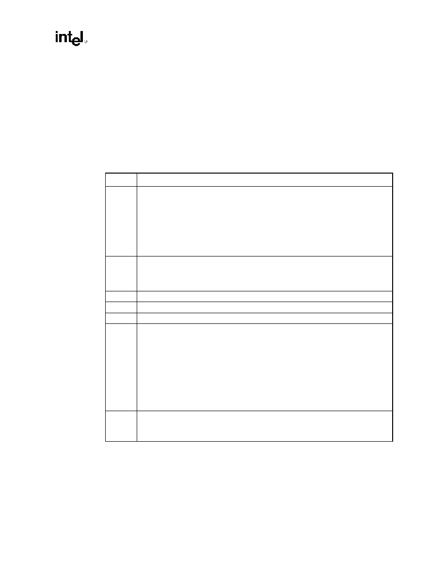
82443GX Host Bridge Datasheet
3-29
Register Description
3.3.21
ESMRAMC--Extended System Management RAM Control
Register (Device 0)
Address Offset:
73h
Default Value:
38h
Access:
Read/Write
Size:
8 bits
The Extended SMRAM register controls the configuration of Extended SMRAM space. The
Extended SMRAM (E_SMRAM) memory provides a write-back cacheable SMRAM memory
space that is above 1 Mbyte.
Bit
Description
7
H_SMRAM_EN (H_SMRAME). Controls the SMM memory space location (i.e above 1 Mbyte or
below 1 Mbyte).
1 = When G_SMRAME is 1 and H SMRAME is set to 1, the High SMRAM memory space is
enabled, the Compatible SMRAM memory is disabled, and accesses in the 0A0000h to
0FFFFFh range are forwarded to PCI, while SMRAM accesses from 100A0000h to
100FFFFFh are remapped to DRAM address A0000h to FFFFFh
0 = When G SMRAME is set to a 1 and H SMRAM EN is set to 0, then the Compatible SMRAM
space is enabled.
Once D_LCK is set, this bit becomes read only.
6
E_SMRAM_ERR (E_SMERR).
1 = This bit is set when CPU accesses the defined memory ranges in Extended SMRAM (High
Memory and T-segment) while not in SMM space and with the D-OPEN bit = 0.
0 = It is software's responsibility to clear this bit. The software must write a 1 to this bit to clear it.
5
SMRAM_Cache (SM_CACHE). This bit is forced to `1' by 82443GX.
4
SMRAM_L1_EN (SM_L1). This bit is forced to `1' by 82443GX.
3
SMRAM_L2_EN (SM_L2). This bit is forced to `1' by 82443GX.
2:1
TSEG_SZ[1:0] (T_SZ). Selects the size of the TSEG memory block, if enabled. This memory is
taken from the top of DRAM space (i.e., TOM - TSEG_SZ), which is no longer claimed by the
memory controller (all accesses to this space are sent to the PCI bus if TSEG_EN is set). The
physical address for the extended SMRAM memory appears is from (256M + TOM - TSEG_SZ) to
(256M + TOM). This address is remapped to DRAM address (TOM - TSEG_SZ) to TOM. This field
decodes as follows:
00 = (TOM≠128KB) to TOM
01 = (TOM≠256KB) to TOM
10 = (TOM≠512KB) to TOM
11 = (TOM≠1MB) to TOM
Once D_LCK is set, this bit becomes read only.
0
TSEG_EN (T_EN). Enabling of SMRAM memory (TSEG, 128 KB, 256 KB, 512 KB or 1 MB of
additional SMRAM memory) for Extended SMRAM space only. When
G_SMRAME =1 and TSEG_EN = 1, the TSEG is enabled to appear in the appropriate physical
address space. Once D_LCK is set, this bit becomes read only.

Register Description
3-30
82443GX Host Bridge Datasheet
3.3.22
RPS--SDRAM Row Page Size Register (Device 0)
Address Offset:
74h≠75h
Default Value:
0000h
Access:
Read/Write
Size:
16 bits
This register sets the row page size for SDRAM.
Bit
Description
15:0
Page Size (PS). Each pair of bits in this register indicate the page size used for one row of DRAM.
The encoding of the two bit fields.
Bits[1:0]
Page Size
00
2 KB
01
4 KB
10
8 KB
11
Reserved
RPS bits
Corresponding DRB register
1:0
DRB[0], row 0
3:2
DRB[1], row 1
5:4
DRB[2], row 2
7:6
DRB[3], row 3
9:8
DRB[4], row 4
11:10
DRB[5], row 5
13:12
DRB[6], row 6
15:14
DRB[7], row 7

82443GX Host Bridge Datasheet
3-31
Register Description
3.3.23
SDRAMC--SDRAM Control Register (Device 0)
Address Offset:
76h≠77h
Default Value:
00h
Access:
Read/Write
Size:
16 bits
Bit
Description
15:8
Reserved
7:5
SDRAM Mode Select (SMS). These bits allow the 82443GX to drive various commands to the
SDRAMs. These special modes are intended for initialization at power up.
SMS
Mode
000
Normal SDRAM Operation. (default)
001
NOP Command Enable. In this mode all CPU cycles to SDRAM result in NOP
Command on the SDRAM interface.
010
All Banks Precharge Enable. In this mode all CPU cycles to SDRAM result in an All
Banks Precharge Command on the SDRAM interface.
011
Mode Register Set Enable. In this mode all CPU cycles to SDRAM result in a mode
register set command on the SDRAM interface. The command is driven on the
MAx[14:0] lines. MAx[2:0] must always be driven to 010 for burst of 4 mode. MA3 must
be driven to 1 for interleave wrap type. MAx4 needs to be driven to the value
programmed in the CAS# Latency bit. MAx[6:5] should always be driven to 01.
MAx[12:7] must be driven to 000000. BIOS must calculate and drive the correct host
address for each row of memory such that the correct command is driven on the
MAx[12:0] lines.
100
CBR Enable. In this mode all CPU cycles to SDRAM result in a CBR cycle on the
SDRAM interface.
101
Reserved.
110
Reserved.
111
Reserved.
Note: BIOS must take into consideration MAB inversion when programming DIMM slots 2 and 3.
4
SDRAMPWR.
0 = Reserved
1 = SDRAMPWR should be set to `1'.
Note: When PCIRST# assertion occurs during POS/STR, these bits are not reset to 0.
3
Leadoff Command Timing (LCT). These bits control when the SDRAM command pins
(SRASx#, SCASx# and WEx#) and CSx# are considered valid on leadoffs for CPU cycles.
0 = 4 CS# Clock
1 = 3 CS# Clock
Note: For all platforms, BIOS should leave the LCT bit set to its default value of 0.
2
CAS# Latency (CL). This bit controls the number of CLKs between when a read command is
sampled by the SDRAMs and when the 82443GX samples read data from the SDRAMs. If a
given row is populated with a registered SDRAM DIMM, an extra clock is inserted between the
read command the when the 82443GX samples read data. For a registered DIMM with CL=2,
this bit should be set to 1.
0 = 3 DCLK CAS# latency.
1 = 2 DCLK CAS# latency.
1
SDRAM RAS# to CAS# Delay (SRCD). This bit controls the number of DCLKs from a Row
Activate command to a read or write command.
0 = 3 clocks will be inserted between a row activate command and either a read or write
command.
1 = 2 clocks will be inserted between a row activate and either a read or write command.
0
SDRAM RAS# Precharge (SRP). This bit controls the number of DCLKs for RAS# precharge.
0 = 3 clocks of RAS# precharge.
1 = 2 clocks of RAS# precharge.

Register Description
3-32
82443GX Host Bridge Datasheet
3.3.24
PGPOL--Paging Policy Register (Device 0)
Address Offset:
78≠79h
Default Value:
0000h
Access:
Read/Write
Size:
16 bits
Bit
Description
15:8
Banks per Row (BPR). Each bit in this field corresponds to one row of the memory array. Bit 15
corresponds to row 7 while bit 8 corresponds to row 0. These bits are defined only for SDRAM
systems and define whether the corresponding row has a two bank implementation or a four
bank implementation. Those with two banks (bit=0) can have up to two pages open at any given
time. Those with four banks (bit=1) can have up to four pages open at any time. Note that the
bits referencing empty rows are `don't care'.
0 = 2 banks
1 = 4 banks
7:5
Reserved.
4
Intel Reserved.
3:0
DRAM Idle Timer (DIT). This field determines the number of clocks that the DRAM controller
will remain in the idle state before precharging all pages.
0000 = 0 clocks
0001 = 2 clocks
0010 = 4 clocks
0011 = 8 clocks
0100 = 10 clocks
0101 = 12 clocks
0110 = 16 clocks
0111 = 32 clocks
1XXX = Infinite (pages are not closed for idle condition).
82443GX Host Bridge Datasheet
3-33
Register Description
3.3.25
PMCR--Power Management Control Register (Device 0)
Address Offset:
7Ah
Default Value:
0000_S0S0b
Access
Read/Write
Size
8 Bits
Bit
Description
7
Intel Reserved
6
ACPI Control Register Enable (SCRE).
1 = Enable. The ACPI control register in the 82443GX is enabled, and all CPU cycles to IO
address 0022h are handled by the 82443GX and are not forwarded to PCI.
0 = Disable (default). All CPU cycles to IO address 0022h are passed on to the PCI bus.
5
Intel Reserved
4
Normal Refresh Enable (NREF_EN). This bit is used to enable normal refresh operation
following a POS/STR state. After coming out of reset the software must set this bit before
doing an access to memory.
1 = Enable
0 = Disable
3
Intel Reserved
2
Gated Clock Enable (GCLKEN). GCLKEN enables internal dynamic clock gating in the
82443GX when a AGPset "IDLE" state occurs. This happens when the 82443GX detects an
idle state on all its buses.
1 = Enable
0 = Disable
1
AGP Disable (AGP_DIS). This register bit is Read Only and a configuration write to it is
ignored.
1 = Disable. The AGP interface and the clocks of AGP associated logic are permanently
disabled. This mode is entered using a strapping option that is sampled by the 82443GX
during reset.
0 = Enable
0
CPU reset without PCIRST enable (CRst_En). This bit enables the 82443GX to assert CPU
reset without an incoming PCIRST#. This option allows the reset of the processor when the
system is coming out of POS state. Defaults to `0' upon PCIRST# assertion.
1 = Enable
0 = Disable
NOTE: When PCIRST# assertion occurs during POS/STR, this bit is not reset to `0'.
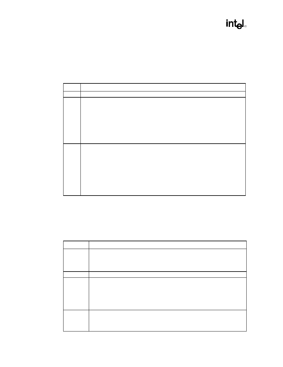
Register Description
3-34
82443GX Host Bridge Datasheet
3.3.26
SCRR--Suspend CBR Refresh Rate Register (Device 0)
Address Offset:
7Bh≠7Ch
Default Value:
0038h
Access
Read/Write
Size
16 Bits
3.3.27
EAP--Error Address Pointer Register (Device 0)
Address Offset:
80≠83h
Default Value:
00000000h
Access
Read Only, Read/Write-Clear
Size
32 Bits
Bit
Description
15:13
Reserved.
12
Suspend CBR refresh Rate Auto Adjust Enable (SRRAEN). SRRAEN bit is cleared to its default
during cold reset only. It is not affected by PCIRST# during resume from suspend.
0 = Disable (default). Indicates that the suspend CBR refresh rate is not updated by the 82443GX
hardware to track the system operating conditions. In this case, it is expected that BIOS will set
the SRR to reflect the worst case operating conditions so that minimum refresh rate will be
provided.
1 = Enable. Indicates that the 82443GX hardware adjusts the suspend refresh rate according to
system operating conditions by comparing the number of OSCCLKs in a given time. This mode
allows the system to dynamically adjust the refresh rate and thus minimize suspend power
consumption while guaranteeing required refresh rate.
11:0
Suspend CBR Refresh Rate (SRR). The rate is loaded into the counter which counts down on
OSCCLK rising edges. When it expires, a suspend CBR refresh request is triggered. This bit field
may be loaded by BIOS to reflect the desirable refresh rate. In addition, the 82443GX will update it
automatically, when the above SRRAEN = 1. In either case, the register is accessible for read and
write operation at all times.
∑
This 12-bit field provides a dynamic range greater than the maximum CBR refresh rate that is
supported of 249.6uSEC.
∑
SRR bit field is cleared to its default during cold reset only. It is not affected by PCIRST# during
resume from suspend.
∑
The default value of this register is 038h, or 56 decimal. It represents a 15.5uS time between
refreshes with the slowest corner OSCCLK cycle time of 270nS.
Bit
Description
31:12
Error Address Pointer (EAP) (RO). This field is used to store the 4 KB block of main memory
of which an error (single bit or multi-bit error) has occurred. Note that this field represents the
address of the first error occurrence after bits 1:0 have been cleared by software. Once bits 1:0
are set to a value different than 00b, as a result of an error, this bit field is locked and doesn't
change as a result of a new error.
11:2
Reserved.
1
Multiple Bit Error (MBE) (R/WC). This bit indicates that a multi-bit ECC error has occurred,
and the address has been logged in bits 31:12. The EAP register is locked until the CPU
clears this bit by writing a 1. Software uses bits 1:0 to detect whether the logged error address
is for Single or Multi bit error, since both Single and Multiple Error bits of the Error Status
register can be set. Once software completes the error processing, a value of `1' is written to
this bit field to clear the value (back to 0) and unlock the error logging mechanism.
Note: Any ECC errors received during initialization should be ignored.
0
Single Bit Error (SBE) (R/WC).
1 = Indicates that a single bit ECC error has occurred, and the address has been logged in bits
31:12. The EAP register is locked until the CPU clears this bit by writing a 1.
Note: Any ECC errors received during initialization should be ignored.

82443GX Host Bridge Datasheet
3-35
Register Description
3.3.28
ERRCMD--Error Command Register (Device 0)
Address Offset:
90h
Default Value:
80h
Access:
Read/Write
Size:
8 bits
This 8-bit register controls the 82443GX responses to various system errors. The actual assertion of
SERR# is enabled via the PCI Command register.
Bit
Description
7
SERR# on AGP Non-Snoopable Access Outside of Graphics Aperture. When enabled and
bit 10 of ERRSTS registers transitions from 0 to 1 (during an AGP access to the address outside
of the graphics aperture) then an SERR# assertion event will be generated.
1 = Enable (default).
0 = Disable.
6
SERR# on Invalid AGP DRAM Access. AGP non-snoopable READ accesses to locations
outside the graphics aperture and outside the main DRAM range (i.e., in 640 KB ≠ 1 MB range or
above top of memory) are invalid. When this bit is set, bit 9 of the ERRSTS will be set and
SERR# will be asserted, read accesses are not directed to main memory or the aperture range.
1 = Enable.
0 = Disable reporting of this condition via SERR#.
5
SERR# on Access to Invalid Graphics Aperture Translation Table Entry. When enabled, the
82443GX sets bit 8 of the ERRSTS and asserts SERR# following a read or write access to an
invalid entry in the Graphics Aperture Translation Table residing in main memory.
1 = Enable.
0 = Disable reporting of this condition via SERR#.
4
SERR# on Receiving Target Abort.
1 = Enable. The 82443GX asserts SERR# on receiving a target abort on either the PCI or AGP.
0 = Disable. The 82443GX does not assert SERR# on receipt of a target abort.
3
SERR# on Detected Thermal Throttling Condition.
1 = Enable. The 82443GX asserts SERR# when thermal throttling condition is detected for either
the read or the write function.
0 = The 82443GX does not assert SERR# for thermal throttling.
2
SERR# Assertion Mode.
1 = SERR# is a level mode signal. Systems that connect SERR# to EXTSMI# for error reporting
should set this bit to 1.
0 = SERR# is asserted for 1 PCI clock (normal PCI mode). (default)
1
SERR# on Receiving Multiple-Bit ECC/Parity Error. When enabled, the 82443GX asserts
SERR# when it detects a multiple-bit error reported by the DRAM controller. For systems not
supporting ECC this bit must be disabled.
1 = Enable.
0 = Disable.
Note: Any ECC errors received during initialization should be ignored.
0
SERR# on Receiving Single-bit ECC Error. When enabled, the 82443GX asserts SERR#
when it detects a single-bit ECC error. For systems not supporting ECC, this bit must be
disabled.
1 = Enable.
0 = Disable.
Note: Any ECC errors received during initialization should be ignored.

Register Description
3-36
82443GX Host Bridge Datasheet
3.3.29
ERRSTS--Error Status Register (Device 0)
Address Offset:
91≠92h
Default Value:
0000h
Access:
Read Only, Read/Write Clear
Size:
16 bits
This 16-bit register is used to report error conditions via the SERR# mechanism. SERR# is
generated on a zero to one transition of any of these flags (if enabled by the ERRCMD register).
Bit
Description
15:13
Reserved.
12
Read thermal Throttling Condition.
1 = Read thermal throttling condition occurred.
0 = Software writes "1" to clear this bit. Default=0
11
Write Thermal Throttling Condition.
1 = Write thermal throttling condition occurred.
0 = Software writes "1" to clear this bit. Default=0
10
AGP non-snoopable access outside of Graphics Aperture.
1 = AGP access occurred to the address that is outside of the graphics aperture range.
0 = Software writes "1" to clear this bit. Default=0
9
Invalid AGP non-snoopable DRAM read access (R/WC).
1 = AGP non-snoopable READ access was attempted outside of the graphics aperture and
outside of main memory (i.e,. in 640 KB ≠ 1 MB range or above top of memory).
0 = Software must write a "1" to clear this status bit.
8
Access to Invalid Graphics Aperture Translation Table Entry (AIGATT) (R\WC).
1 = An invalid translation table entry was returned in response to a graphics aperture read or write
access.
0 = Software must write a "1" to clear this bit.
7:5
Multi-bit First Error (MBFRE) (RO). This field contains the encoded value of the DRAM row in
which the first multi-bit error occurred. A simple binary encoding is used to indicate the row
containing the multi-bit error. When an error is detected, this field is updated and the MEF bit is set.
This field will then be locked (no further updates) until the MEF flag has been reset. If MEF is 0, the
value in this field is undefined.
000 = Row 0
001 = Row 1
...
111 = Row 7
4
Multiple-bit ECC (uncorrectable) Error Flag (MEF) (R/WC).
1 = Memory data transfer had an uncorrectable error(i.e., multiple-bit error). When enabled, a
multiple bit error is reported by the DRAM controller and propagated to the SERR# pin, if
enabled by bit 1 in the ERRCMD register.
0 = BIOS writes a 1 to clear this bit and unlock the MBFRE field. (Default = 0).
3:1
Single-bit First Row Error (SBFRE) (RO). This field contains the encoded value of the DRAM row
in which the first single-bit error occurred. A simple binary encoding is used to indicate the row
containing the single-bit error. When an error is detected, this field is updated and SEF is set. This
field is then locked (no further updates) until the SEF flag has been reset. If SEF is 0, the value in
this field is undefined.
000 = Row 0
001 = Row 1
...
111 = Row 7
0
Single-bit (correctable) ECC Error Flag (SEF) (R/WC).
1 = Memory data transfer had a single-bit correctable error and the corrected data was sent for the
access. When ECC is enabled, a single bit error is reported and propagated to the SERR# pin,
if enabled by bit 0 in the ERRCMD register.
0 = BIOS writes a 1 to clear this bit and unlock the SBFRE field.
82443GX Host Bridge Datasheet
3-37
Register Description
3.3.30
ACAPID--AGP Capability Identifier Register (Device 0)
Address Offset:
A0≠A3h
Default Value:
00100002h/00000000h
Access:
Read Only
Size:
32 bits
This register provides normal identifier for AGP capability.
3.3.31
AGPSTAT--AGP Status Register (Device 0)
Address Offset:
A4≠A7h
Default Value:
1F000203h
Access:
Read Only
Size:
32 bits
This register reports AGP compliant device capability/status.
Bit
Description
31:24
Reserved
23:20
Major AGP Revision Number. This field provides a major revision number of AGP specification to
which this version of the 82443GX conforms. When the AGP DIS bit (PMCR[1]) is set to 0, this
number is set to value of "0001b" (i.e., implying Rev 1.x). When the AGP DIS bit (PMCR[1]) is set
to 1, This number is set to "0000b".
19:16
Minor AGP Revision Number. These bits provide a minor revision number of AGP specification
to which this version of 82443GX conforms. This number is hardwired to value of "0000" (i.e.,
implying Rev x.0). Together with major revision number this field identifies 82443GX as an AGP
REV 1.0 compliant device.
15:8
Next Capability Pointer. AGP capability is the first and the last capability described via the
capability pointer mechanism.
0s = Hardwired to 0s to indicate the end of the capability linked list.
7:0
AGP Capability ID. This field identifies the linked list item as containing AGP registers. When the
AGP DIS bit (PMCR[1]) is set to 0, this field has a value of 0000_0010b assigned by the PCI SIG.
When the AGP DIS bit (PMCR[1]) is set to 1, this field has a value of 00h.
Bit
Description
31:24
AGP Maximum Request Queue Depth (RO). This field is hardwired to 1Fh to indicate a
maximum of 32 outstanding AGP command requests can be handled by the 82443GX.
23:10
Reserved
9
AGP Side Band Addressing Supported. This bit indicates that the 82443GX supports side band
addressing. It is hardwired to 1.
8:2
Reserved
1:0
AGP Data Transfer Type Supported (R/W). Bit 0 identifies if AGP compliant device supports 1x
data transfer mode and bit 1 identifies if AGP compliant device supports 2x data transfer mode.
Configuration software will update this field by setting only one bit that corresponds to the
capability of AGP master (after that capability has been verified by accessing the same functional
register within the AGP masters configuration space).
00 = Not allowed
01 = 1x data transfer mode supported
10 = 2x data transfer mode supported
11 = (default)
NOTE: The selected data transfer mode apply to both AD bus and SBA bus.

Register Description
3-38
82443GX Host Bridge Datasheet
3.3.32
AGPCMD--AGP Command Register (Device 0)
Address Offset:
A8≠ABh
Default Value:
00000000h
Access:
Read/Write
Size:
32 bits
This register provides control of the AGP operational parameters.
Bit
Description
31:10
Reserved.
9
AGP Side Band Enable. This bit enables the side band addressing mechanism.
1 = Enable.
0 = Disable.
8
AGP Enable. When disabled, the 82443GX ignores all AGP operations, including the sync
cycle. Any AGP operations received while this bit is set to 1 is serviced even if this bit is reset
to 0. If this bit transitions from a 1 to a 0 on a clock edge in the middle of an SBA command
being delivered in 1X mode the command will be issued. When this bit is set to 1 the
82443GX will respond to AGP operations delivered via PIPE#, or to operations delivered via
SBA if the AGP Side Band Enable bit is also set to 1.
The AGP parameters in the AGPCMD and AGPCTRL registers must be set prior to setting
this bit `1'. With the exception of the GTLB_ENABLE (bit 7, AGPCTRL), and ATTBASE
register (offset B8h), which can be modified dynamically.
1 = Enable.
0 = Disable.
7:2
Reserved.
1:0
AGP Data Transfer Rate. One (and only one) bit in this field must be set to indicate the
desired data transfer rate (Bit 0 for 1X, Bit 1 for 2X). The same bit must be set on both master
and target. Configuration software will update this field by setting only one bit that
corresponds to the capability of AGP master (after that capability has been verified by
accessing the same functional register within the AGP masters configuration space.)
00 = default
01 = 1x data transfer rate.
10 = 2x data transfer rate.
11 = Illegal
NOTE: This field applies to AD and SBA buses.

82443GX Host Bridge Datasheet
3-39
Register Description
3.3.33
AGPCTRL--AGP Control Register (Device 0)
Address Offset:
B0≠B3h
Default Value:
00000000h
Access:
Read/Write
Size:
32 bits
This register provides for additional control of the AGP interface.
Bit
Description
31:16
Reserved.
15
Snoopable Writes In Order With AGP Reads Disable (AGPDCD). When set to 0 (default), the
82443GX maintains ordering between snoopable write cycles and AGP reads. When set to 1, the
82443GX handles the AGP reads and snoopable writes as independent streams.
AGPDCD
AGPRSE
Description
(Bit 15)
(Bit 13)
0
0
DWB is visible to AGP reads. DWB flushes only when address hit.
0
1
Illegal.
1
0
Illegal
1
1
DWB flushes when write to AGP occurs
14
Reserved
13
Graphics Aperture Write-AGP Read Synchronization Enable (AGPRSE). When this bit is set
the 82443GX will ensure that all writes posted in the Global Write Buffer to the Graphics Aperture
are retired to DRAM before the 82443GX will initiate any CPU-to-AGP cycle. This can be used to
ensure synchronization between the CPU and AGP master. The AGPDCD bit description defines
the interaction between the AGPRSE bit and the AGPDCD bit.
1 = Enable
0 = Disable (Default)
12:8
Reserved
7
GTLB Enable (and GTLB Flush Control).
1 = Enable. Normal operations of the Graphics Translation Lookaside Buffer.
0 = Disable (default). The GTLB is flushed by clearing the valid bits associated with each entry.
6:0
Reserved.

Register Description
3-40
82443GX Host Bridge Datasheet
3.3.34
APSIZE--Aperture Size Register (Device 0)
Address Offset:
B4h
Default Value:
00h
Access:
Read/Write
Size:
8 bits
This register determines the effective size of the Graphics Aperture used for a particular 82443GX
configuration. This register can be updated by the 82443GX-specific BIOS configuration sequence
before the PCI normal bus enumeration sequence takes place. If the register is not updated, a
default value selects an aperture of maximum size (i.e., 256 MB). The size of the table that will
correspond to a 256 MB aperture is not practical for most applications and, therefore, these bits
must be programmed to a smaller practical value that forces adequate address range to be requested
via the APBASE register from the PCI configuration software.
3.3.35
ATTBASE--Aperture Translation Table Base Register
(Device 0)
Address Offset:
B8≠BBh
Default Value:
00000000h
Access:
Read/Write
Size:
32 bits
This register provides the starting address of the Graphics Aperture Translation Table base located
in the main DRAM. The ATTBASE register may be dynamically changed.
Note:
The address provided via ATTBASE is 4KB aligned.
Bit
Description
7:6
Reserved.
5:0
Graphics Aperture Size (APSIZE) (R/W). Each bit in APSIZE[5:0] operates on similarly ordered
bits in APBASE[27:22] of the Aperture Base configuration register. When a particular bit of this field
is "0", it forces the similarly ordered bit in APBASE[27:22] to behave as "hardwired" to 0. When a
particular bit of this field is set to "1", it allows corresponding bit of the APBASE[27:22] to be read/
write accessible. Only the following combinations are allowed:
11 1111 = 4 MB
11 1110 = 8 MB
11 1100 = 16 MB
11 1000 = 32 MB
11 0000 = 64 MB
10 0000 = 128 MB
00 0000 = 256MB
Default for APSIZE[5:0]=000000b forces default APBASE[27:22] =000000b (i.e., all bits respond as
"hardwired" to 0). This provides maximum aperture size of 256 MB. As another example,
programming APSIZE[5:0]=111000b hardwires APBASE[24:22]=000b and while enabling
APBASE[27:25] as read/write programmable.
Bit
Description
31:12
Aperture Translation Table Base Address. Bits 31:12 correspond to address bits 31:12,
respectively. This field contains a pointer to the base of the translation table used to map memory
space addresses in the aperture range to addresses in main memory.
11:0
Reserved.

82443GX Host Bridge Datasheet
3-41
Register Description
3.3.36
MBFS--Memory Buffer Frequency Select Register
(Device 0)
Address Offset:
CA≠CCh
Default Value:
000000h
Access:
Read/Write
Size:
24 bits
The settings in this register enable the 100 MHz buffers for each of the following signal groups.
Bit
Description
23
Reserved
22
MAA[14:0], WEA#, SRASA#, SCASA#. This bit enables 100 MHz buffers for MAA[14:0], WEA#,
SRASA#, SCASA#.
0 = Reserved
1 = 100 MHz
21
MAB[12:11, 9:0]# & MAB[14,13,10], WEB#, SRASB#, SCASB#. This bit enables 100 MHz
buffers for MAB[12:11, 9:0]# & MAB[14,13,10], WEB#, SRASB#, SCASB#. Note that the
address's MABx# are inverted copies of MAA, with the exception of MAB[14,13,10].
0 = Reserved
1 = 100 MHz
20
MD [63:0] [Control 2]). This bit enables 100 MHz buffers for MD [63:0] [Control 2]. (Refer to the
corresponding MBSC register for programming details).
0 = Reserved
1 = 100 MHz
19
MD [63:0] [Control 1]. This bit enables 100 MHz buffers for MD [63:0] [Control 1]. (Refer to the
corresponding MBSC register for programming details).
0 = 100 MHz A
1 = 100 MHz B
18
MECC [7:0] [Control 2]. This bit enables 100 MHz buffers for MECC [7:0] [Control 2]. (Refer to
the corresponding MBSC register for programming details).
0 = 100 MHz A
1 = 100 MHz B
17
MECC [7:0] [Control 1). This bit enables 100 MHz buffers for MECC [7:0] [Control 1]. (Refer to
the corresponding MBSC register for programming details).
0 = Reserved
1 = 100 MHz
16
CSB7#. This bit enables 100 MHz buffers for CSB7#.
0 = Reserved
1 = 100 MHz
15
CSA7#. This bit enables 100 MHz buffers for CSA7#.
0 = Reserved
1 = 100 MHz
14
CSB6#. This bit enables 100 MHz buffers for CSB6#.
0 = Reserved
1 = 100 MHz
13
CSA6#. This bit enables 100 MHz buffers for CSA6#.
0 = Reserved
1 = 100 MHz
Register Description
3-42
82443GX Host Bridge Datasheet
3.3.37
BSPAD--BIOS Scratch Pad Register (Device 0)
Address Offset:
D0≠D7h
12
CSA5#, CSB5#. This bit enables 100 MHz buffers for CSA5#, CSB5#.
0 = Reserved
1 = 100 MHz
11
CSA4#, CSB4#. This bit enables 100 MHz buffers for CSA4#, CSB4#.
0 = Reserved
1 = 100 MHz
10
CSA3#, CSB3#. This bit enables 100 MHz buffers for CSA3#, CSB3#.
0 = Reserved
1 = 100 MHz
9
CSA2#, CSB2#. This bit enables 100 MHz buffers for CSA2#, CSB2#.
0 = Reserved
1 = 100 MHz
8
CSA1#, CSB1#. This bit enables 100 MHz buffers for CSA1#, CSB1#.
0 = Reserved
1 = 100 MHz
7
CSA0#, CSB0#. This bit enables 100 MHz buffers for CSA0#, CSB0#.
0 =Reserved
1 = 100 MHz
6
DQMA5. This bit enables 100 MHz buffers for DQMA5.
0 = Reserved
1 = 100 MHz
5
DQMA1. This bit enables 100 MHz buffers for DQMA1.
0 = Reserved
1 = 100 MHz
4
DQMB5. This bit enables 100 MHz buffers for DQMB5.
0 = Reserved
1 = 100 MHz
3
DQMB1. This bit enables 100 MHz buffers for DQMB1.
0 = Reserved
1 = 100 MHz
2
DQMA[7:6,4:2,0]. This bit enables 100 MHz buffers for DQMA[7:6], DQMA[4:2], and DQMA[0].
0 = Reserved
1 = 100 MHz
1
GCKE. This bit enables 100 MHz buffers for GCKE.
0 = Reserved
1 = 100 MHz
0
FENA. This bit enables 100 MHz buffers for FENA.
0 = Reserved
1 = 100 MHz
Bit
Description
82443GX Host Bridge Datasheet
3-43
Register Description
Default Value:
0000-0000-0000-0000h
Access:
Read/Write
Size:
64 bits
This register provides 8 bytes general purpose read/write registers for the BIOS to perform the
configuration routine. The 82443GX will provide this 8 byte register in the PCI configuration space
of the 82443GX device0 on bus 0. The registers in this range will be defined as read/write and will
be initialized to all 0's after PCIRST#. The BIOS will can access these registers through the normal
PCI configuration register mechanism, accessing 1,2 or 4 bytes in every data access.
3.3.38
DWTC--DRAM Write Thermal Throttling Control Register
(Device 0)
Offset:
E0h≠E7h
Default:
0000_0000_0000_0000h
Access:
Read/Write/Lock
Size:
64 bits
A locking mechanism is included to protect contents of this register as well as the DRAM Read
Thermal Throttling Control register described below.
Bit
Description
64:0
BIOS Work Space.
Bits
Description
63
Throttle Lock (TLOCK). This bit secures the DRAM thermal throttling control registers.
1 = All configuration register bits in E0h≠E7h & E8h≠EFh (read throttle control) are read-only.
0 = Default
62:46
Reserved
45:38
Global DRAM Write Sampling Window (GDWSW). This 8-bit value is multiplied by 4 to define
the length of time in milliseconds (0≠1020) over which the number of QWords written is counted.
37:26
Global QWord Threshold (GQT). The 12-bit value held in this field is multiplied by 215 to arrive
at the number of QWords that must be written within the Global DRAM Write Sampling Window in
order to cause the thermal throttling mechanism to be invoked.
25:20
Throttle Time (TT). This value provides a multiplier between 0 and 63 which specifies how long
thermal throttling remains in effect as a number of Global DRAM Write Sampling Windows. For
example, if GDWSW is programmed to 1000_0000b and TT is set to 01_0000b, then thermal
throttling will be performed for ~2 seconds once invoked (128 ms * 16).
19:13
Throttle Monitoring Window (TMW). The value in this register is padded with four 0's to specify
a window of 0≠2047 DRAM CLKs with 16 clock granularity. While the thermal throttling
mechanism is invoked, DRAM writes are monitored during this window--if the number of QWords
written during the window reaches the Throttle QWord Maximum, then write requests are blocked
for the remainder of the window.
12:3
Throttle QWord Maximum (TQM). The Throttle QWord Maximum defines the maximum number
of QWords between 0≠1023 which are permitted to be written to DRAM within one Throttle
Monitoring Window while the thermal throttling mechanism is in effect.
2:0
DRAM Write Throttle Mode. Normal DRAM write monitoring and thermal throttling operation are
enabled when bits 2:0 are set to 100. All other combinations are Intel Reserved.
000-011 = Intel Reserved
100 = Normal Operations
101-111 = Intel Reserved
Register Description
3-44
82443GX Host Bridge Datasheet
3.3.39
DRTC--DRAM Read Thermal Throttling Control Register
(Device 0)
Offset:
E8h≠EFh
Default:
0000_0000_0000_0000h
Access:
Read/Write/Lock
Size:
64 Bits
The contents of this register are protected by making the bits read-only once a `1' is written to the
Throttle Lock bit (bit 63 of configuration register E0≠E7h)
Bits
Description
63:46
Reserved
45:38
Global DRAM Read Sampling Window (GDRSW). This 8-bit value is multiplied by 4 to define
the length of time in milliseconds (0≠1020) over which the number of QWords read from DRAM is
counted.
37:26
Global Read QWord Threshold (GRQT). The 12-bit value held in this field is multiplied by 215 to
arrive at the number of QWords that must be written within the Global DRAM Read Sampling
Window in order to cause the thermal throttling mechanism to be invoked.
25:20
Read Throttle Time (RTT). This value provides a multiplier between 0 and 63 which specifies
how long read thermal throttling remains in effect as a number of Global DRAM Read Sampling
Windows. For example, if GDRSW is programmed to 1000_0000b and RTT is set to 01_0000b,
then read thermal throttling will be performed for ~2 seconds once invoked (128 ms * 16).
19:13
Read Throttle Monitoring Window (RTMW). The value in this register is padded with 4 0's to
specify a window of 0≠2047 DRAM CLKs with 16 clock granularity. While the thermal throttling
mechanism is invoked, DRAM reads are monitored during this window--if the number of QWords
read during the window reaches the Throttle QWord Maximum, then Host and PCI read requests,
as well as all AGP requests, are blocked for the remainder of the window.
12:3
Read Throttle QWord Maximum (RTQM). The Read Throttle QWord Maximum defines the
maximum number of QWords between 0≠1023 which are permitted to be read from DRAM within
one Read Throttle Monitoring Window while thermal throttling mechanism is in effect.
2:0
DRAM Read Throttle Mode. Normal DRAM read monitoring and thermal throttling operation are
enabled when bits 2:0 are set to 100. All other combinations are Intel Reserved.
000-011 = Intel Reserved
100 = Normal Operations
101-111 = Intel Reserved

82443GX Host Bridge Datasheet
3-45
Register Description
3.3.40
BUFFC--Buffer Control Register (Device 0)
Offset:
F0≠F1h
Default:
0000h
Access:
Read/Write
Size:
16 bits
The Jam Latch design provides the AGP sub-system with a variable strength, to better
accommodate the clamping requirements.
The Jam Latch Register should be enabled by the BIOS during the resume sequence from STR, if
these Jam Latch control bits had been enabled before the STR was executed.
Bit
Description
15:10
Reserved.
9:6
AGP Jam Latch Strength Select.
Bit 9 = 1; Enable strong pull-up
Bit 8 = 1; Enable weak pull-up
Bit 7 = 1; Enable strong pull-down
Bit 6 = 1; Enable weak pull-down
5:0
Intel Reserved.

Register Description
3-46
82443GX Host Bridge Datasheet
3.4
PCI-to-PCI Bridge Registers (Device 1)
The configuration space for device #1 is controlled by the AGP_DIS bit in the PMCR register.
Note:
When AGP_DIS = 0, the configuration space for device #1 is enabled, and the registers defined
below are accessible through the configuration mechanism defined in the first section of this
document.
Note:
When the AGP_DIS = 1, the configuration space for device #1 is disabled. All configuration cycles
(reads and writes) to device #1 of bus 0 will cause the master abort status bit for device #0/ bus 0 to
be set. Configuration read cycles will return data of all 1's. Configuration write cycles will have no
effect on the registers.
Table 3-4. 82443GX Configuration Space--Device 1
Address
Offset
Register
Symbol
Register Name
Default
Value
Access
00≠01h
VID1
Vendor Identification
8086h
RO
02≠03h
DID1
Device Identification
71A1h
RO
04≠05h
PCICMD1
PCI Command Register
0000h
R/W
06≠07h
PCISTS1
PCI Status Register
0220h
RO, R/WC
08h
RID1
Revision Identification
00h
RO
09h
--
Reserved
00h
--
0Ah
SUBC1
Sub-Class Code
04h
RO
0Bh
BCC1
Base Class Code
06h
RO
0Ch
--
Reserved
00h
--
0Dh
MLT1
Master Latency Timer
00h
R/W
0Eh
HDR1
Header Type
01h
RO
0F≠17h
--
Reserved
00h
--
18h
PBUSN
Primary Bus Number
00h
RO
19h
SBUSN
Secondary Bus Number
00h
R/W
1Ah
SUBUSN
Subordinate Bus Number
00h
R/W
1Bh
SMLT
Secondary Bus Master Latency Timer
00h
R/W
1Ch
IOBASE
I/O Base Address Register
F0h
R/W
1Dh
IOLIMIT
I/O Limit Address Register
00h
R/W
1E≠1Fh
SSTS
Secondary PCI-to-PCI Status Register
02A0h
R/WC, RO
20≠21h
MBASE
Memory Base Address Register
FFF0h
R/W
22≠23h
MLIMIT
Memory Limit Address Register
0000h
R/W
24≠25h
PMBASE
Prefetchable Memory Base Address Reg.
FFF0h
R/W
26≠27h
PMLIMIT
Prefetchable Memory Limit Address Reg.
0000h
R/W
28≠3Dh
--
Reserved
0
c
3Eh
BCTRL
Bridge Control Register
80h
R/W
3F≠FFh
--
Reserved
00h
--

82443GX Host Bridge Datasheet
3-47
Register Description
3.4.1
VID1--Vendor Identification Register (Device 1)
Address Offset:
00≠01h
Default Value:
8086h
Attribute:
Read Only
Size:
16 bits
The VID Register contains the vendor identification number. This 16-bit register combined with
the Device Identification Register uniquely identify any PCI device. Writes to this register have no
effect.
3.4.2
DID1--Device Identification Register (Device 1)
Address Offset:
02≠03h
Default Value:
71A1h
Attribute:
Read Only
Size:
16 bits
This 16-bit register combined with the Vendor Identification register uniquely identifies any PCI
device. Writes to this register have no effect.
Bit
Description
15:0
Vendor Identification Number. This is a 16-bit value assigned to Intel. Intel VID = 8086h.
Bit
Description
15:0
Device Identification Number. This is a 16 bit value assigned to the 82443GX device #1.
82443GX device #1 DID =71A1h.

Register Description
3-48
82443GX Host Bridge Datasheet
3.4.3
PCICMD1--PCI-to-PCI Command Register (Device 1)
Address Offset:
04≠05h
Default:
0000h
Access:
Read/Write
Size
16 bits
Bit
Descriptions
15:10
Reserved.
9
Fast Back-to-Back: Not Applicable. Hardwired to 0.
8
SERR# Enable (SERRE1). When enabled the SERR# signal driver (common for PCI and AGP)
is enabled for error conditions that occur on AGP.If both SERRE and SERRE1 are reset to 0,
then SERR# is never driven by the 82443GX. Also, if this bit is set and the Parity Error Response
Enable Bit (Dev 01h, Register 3Eh, Bit 0) is set, then the 82443GX will report ADDRESS and
DATA parity errors on AGP.
1 = Enable.
0 = Disable.
7
Address/Data Stepping. Not applicable. Hardwired to 0.
6
Parity Error Enable (PERRE1). Hardwired to 0.
5
Reserved.
4
Memory Write and Invalidate Enable: Not applicable. However, supported as a read/write bit
to avoid the problems with normal PCI-to-PCI Bridge configuration software.
3
Special Cycle Enable: Not applicable. However, supported as a read/write bit to avoid the
problems with normal PCI-to-PCI Bridge configuration software.
2
Bus Master Enable (BME1): Not applicable. However, supported as a read/write bit to avoid
the problems with normal PCI-to-PCI Bridge configuration software.
1
Memory Access Enable (MAE1): Not applicable. However, supported as a read/write bit to
avoid the problems with normal PCI-to-PCI Bridge configuration software.
0
I/O Access Enable (IOAE1): Not applicable. However, supported as a read/write bit to avoid
the problems with normal PCI-to-PCI Bridge configuration software.

82443GX Host Bridge Datasheet
3-49
Register Description
3.4.4
PCISTS1--PCI-to-PCI Status Register (Device 1)
Address Offset:
06≠07h
Default Value:
0220h
Access:
Read Only, Read/Write Clear
Size:
16 bits
PCISTS1 is a 16-bit status register that reports the occurrence of error conditions associated with
primary side of the "virtual" PCI-to-PCI bridge embedded within the 82443GX.
3.4.5
RID1--Revision Identification Register (Device 1)
Address Offset:
08h
Default Value:
00/01h
Access:
Read Only
Size:
8 bits
This register contains the revision number of the 82443GX device #1. These bits are read only and
writes to this register have no effect.
Bit
Descriptions
15
Detected Parity Error (DPE1). Not Applicable. Hardwired to 0.
14
Reserved.
13
Received Master Abort Status (RMAS1). Not Applicable. Hardwired to 0.
12
Received Target Abort Status (RTAS1). Not Applicable. Hardwired to 0.
11
Signaled Target Abort Status (STAS1). Not Applicable. Hardwired to 0.
10:9
DEVSEL# Timing (DEVT1). Not Applicable. Hardwired to "01b".
8
Data Parity Detected (DPD1). Not Applicable. Hardwired to 0.
7
Fast Back-to-Back (FB2B1). Not Applicable. Hardwired to 0.
6
Reserved.
5
66/60 MHz Capability. Hardwired to "1".
4:0
Reserved.
Bit
Description
7:0
Revision Identification Number. This is an 8-bit value that indicates the revision identification
number for the 82443GX device #1.
A-0 = 00h
Register Description
3-50
82443GX Host Bridge Datasheet
3.4.6
SUBC1--Sub-Class Code Register (Device 1)
Address Offset:
0Ah
Default Value:
04h
Access:
Read Only
Size:
8 bits
This register contains the Sub-Class Code for the 82443GX device #1. This code is 04h indicating
a PCI-to-PCI Bridge device. The register is read only.
3.4.7
BCC1--Base Class Code Register (Device 1)
Address Offset:
0Bh
Default Value:
06h
Access:
Read Only
Size:
8 bits
This register contains the Base Class Code of the 82443GX device #1. This code is 06h indicating
a Bridge device. This register is read only.
3.4.8
MLT1--Master Latency Timer Register (Device 1)
Address Offset:
0Dh
Default Value:
00h
Access:
Read/Write
Size:
8 bits
This functionality is not applicable. It is described here since these bits should be implemented as a
read/write to comply with the normal PCI-to-PCI bridge configuration software.
Bit
Description
7:0
Sub-Class Code (SUBC1). This is an 8-bit value that indicates the category of Bridge into which
the 82443GX falls.
04h = Host Bridge.
Bit
Description
7:0
Base Class Code (BASCC). This is an 8-bit value that indicates the Base Class Code for the
82443GX device #1.
06h = Bridge device.
Bit
Description
7:3
Not applicable but support read/write operations. (Reads return previously written data.)
2:0
Reserved.

82443GX Host Bridge Datasheet
3-51
Register Description
3.4.9
HDR1--Header Type Register (Device 1)
Offset:
0Eh
Default:
01h
Access:
Read Only
Size:
8 bits
This register identifies the header layout of the configuration space. No physical register exists at
this location.
3.4.10
PBUSN--Primary Bus Number Register (Device 1)
Offset:
18h
Default:
00h
Access:
Read Only
Size:
8 bits
This register identifies that "virtual" PCI-to-PCI bridge is connected to bus #0.
3.4.11
SBUSN--Secondary Bus Number Register (Device 1)
Offset:
19h
Default:
00h
Access:
Read /Write
Size:
8 bits
This register identifies the bus number assigned to the second bus side of the "virtual" PCI-to-PCI
bridge i.e. to AGP. This number is programmed by the PCI configuration software to allow
mapping of configuration cycles to AGP.
Bit
Descriptions
7:0
Header Type (HEADT). This read only field always returns 01h when read. Writes have no effect.
Bit
Descriptions
7:0
Bus Number. Hardwired to "0".
Bit
Descriptions
7:0
Bus Number. Programmable
Default "0".

Register Description
3-52
82443GX Host Bridge Datasheet
3.4.12
SUBUSN--Subordinate Bus Number Register (Device 1)
Offset:
1Ah
Default:
00h
Access:
Read /Write
Size:
8 bits
This register identifies the subordinate bus (if any) that resides at the level below AGP.This number
is programmed by the PCI configuration software to allow mapping of configuration cycles to AGP.
3.4.13
SMLT--Secondary Master Latency Timer Register
(Device 1)
Address Offset:
1Bh
Default Value:
00h
Access:
Read/Write
Size:
8 bits
This register control the bus tenure of the 82443GX on AGP the same way the Device 0 MLT
controls the access to the PCI bus.
3.4.14
IOBASE--I/O Base Address Register (Device 1)
Address Offset:
1Ch
Default Value:
F0h
Access:
Read/Write
Size:
8 bits
This register control the CPU to AGP I/O access routing based on the following formula:
IO_BASE=< address =<IO_LIMIT
3.4.15
IOLIMIT--I/O Limit Address Register (Device 1)
Address Offset:
1Dh
Default Value:
00h
Access:
Read/Write
Size:
8 bits
This register controls the CPU to AGP I/O access routing based on the following formula:
IO_BASE=< address =<IO_LIMIT
Bit
Descriptions
7:0
Bus Number. Programmable.
Bit
Description
7:3
Secondary MLT Counter Value. The default is 0s (i.e,. SMLT disabled)
2:0
Reserved.
Bit
Description
7:4
I/O Address Base. Corresponds to A[15:12] of the I/O address. Default = Fh
3:0
Reserved.

82443GX Host Bridge Datasheet
3-53
Register Description
3.4.16
SSTS--Secondary PCI-to-PCI Status Register (Device 1)
Address Offset:
1E≠1Fh
Default Value:
02A0h
Access:
Read Only, Read/Write Clear
Size:
16 bits
SSTS is a 16-bit status register that reports the occurrence of error conditions associated with
secondary side (i.e. AGP side) of the "virtual" PCI-to-PCI bridge embedded within 82443GX.
Bit
Description
7:4
I/O Address Limit. Corresponds to A[15:12] of the I/O address. Default=0
3:0
Reserved. (Only 16 bit addressing supported.)
Bit
Descriptions
15
Detected Parity Error (DPE1). Note that the PERRE1 bit does not affect the function of this bit.
Also the PERR# is not implemented in the 82443GX.
1 = 82443GX detected of a parity error in the address or data phase of AGP bus transactions.
0 = Software sets DPE1 to 0 by writing a 1 to this bit.
14
Received System Error (SSE1).
1 = 82443GX asserted SERR# for any enabled error condition under device 1. Device 1 error
conditions are enabled in the SSTS and BCTRL registers.
0 = Software clears SSE1 to 0 by writing a 1 to this bit.
13
Received Master Abort Status (RMAS1).
1 = 82443GX terminates a Host-to-AGP with an unexpected master abort.
0 = Software resets this bit to 0 by writing a 1 to it.
12
Received Target Abort Status (RTAS1).
1 = 82443GX-initiated transaction on AGP is terminated with a target abort.
0 = Software resets RTAS1 to 0 by writing a 1 to it.
11
Signaled Target Abort Status (STAS1). STAS1 is hardwired to a 0, since the 82443GX does not
generate target abort on AGP.
10:9
DEVSEL# Timing (DEVT1). This 2-bit field indicates the timing of the DEVSEL# signal when the
82443GX responds as a target on AGP, and is hard-wired to the value 01b (medium) to indicate
the time when a valid DEVSEL# can be sampled by the initiator of the PCI cycle.
01 = Medium. (hardwired)
8
Data Parity Detected (DPD1). Hardwired to 0. 82443GX does not implement G_PERR# function.
However, data parity errors are still detected and reported on SERR# (if enabled by SERRE,
SERRE1 and the BCTRL register, bit 0).
7
Fast Back-to-Back (FB2B1). This bit is hardwired to 1. The 82443GX as a target supports fast
back-to-back transactions on AGP.
6
Reserved.
5
66/60MHZ Capability. Hardwired to 1.
4:0
Reserved.

Register Description
3-54
82443GX Host Bridge Datasheet
3.4.17
MBASE--Memory Base Address Register (Device 1)
Address Offset:
20≠21h
Default Value:
FFF0h
Access:
Read/Write
Size:
16 bits
This register controls the CPU to AGP non-prefetchable memory access routing based on the
following formula:
MEMORY_BASE=< address =<MEMORY_LIMIT
This register must be initialized by the configuration software.
3.4.18
MLIMIT--Memory Limit Address Register (Device 1)
Address Offset:
22≠23h
Default Value:
0000h
Access:
Read/Write
Size:
16 bits
This register controls the CPU to AGP non-prefetchable memory access routing based on the
following formula:
MEMORY_BASE=< address =<MEMORY_LIMIT
This register must be initialized by the configuration software.
Note:
Memory range covered by MBASE and MLIMIT registers are used to map non-prefetchable AGP
address ranges (typically where control/status memory-mapped I/O data structures of the graphics
controller will reside) and PMBASE and PMLIMIT are used to map prefetchable address ranges
(typically graphics local memory). This segregation allows application of USWC space attribute to
be performed in a true plug-and-play manner to the prefetchable address range for improved CPU-
AGP memory access performance.
Note:
The configuration software is responsible for programming all address range registers
(prefetchable, non-prefetchable) with the values that provide exclusive address ranges i.e. prevent
overlap with each other and/or with the ranges covered with the main memory. There is no
provision in the 82443GX hardware to enforce prevention of overlap and operations of the system
in the case of overlap are not guaranteed.
Bit
Description
15: 4
Memory Address Base (MEM_BASE). Corresponds to A[31:20] of the memory address.
Default=FFF0h
3:0
Reserved.
Bit
Description
15: 4
Memory Address Limit (MEM_LIMIT). Corresponds to A[31:20] of the memory address. Default=0
3:0
Reserved.
82443GX Host Bridge Datasheet
3-55
Register Description
3.4.19
PMBASE--Prefetchable Memory Base Address Register
(Device 1)
Address Offset:
24≠25h
Default Value:
FFF0h
Access:
Read/Write
Size:
16 bits
This register controls the CPU to AGP prefetchable memory accesses routing based on the
following formula:
PREFETCHABLE_MEMORY_BASE=< address =<PREFETCHABLE_MEMORY_LIMIT
This register must be initialized by the configuration software.
3.4.20
PMLIMIT--Prefetchable Memory Limit Address Register
(Device 1)
Address Offset:
26≠27h
Default Value:
0000h
Access:
Read/Write
Size:
16 bits
This register controls the CPU to AGP prefetchable memory accesses routing based on the
following formula:
PREFETCHABLE_MEMORY_BASE=< address =<PREFETCHABLE_MEMORY_LIMIT
This register must be initialized by the configuration software.
Note:
The prefetchable memory range is supported to allow segregation by the configuration software
between the memory ranges that must be defined as Uncachable and the ones that can be
designated as a USWC (i.e. prefetchable) from the CPU perspective.
Bit
Description
15: 4
Prefetchable Memory Address Base(PMEM_BASE).Corresponds to A[31:20] of the memory
address.
Default=FFF0h
3:0
Reserved.
Bit
Description
15: 4
Prefetchable Memory Address Limit (PMEM_LIMIT). Corresponds to A[31:20] of the memory
address. Default=0
3:0
Reserved.

Register Description
3-56
82443GX Host Bridge Datasheet
3.4.21
BCTRL--PCI-to-PCI Bridge Control Register (Device 1)
Address Offset:
3Eh
Default:
80h
Access:
Read/Write
Size
8 bits
This register provides extensions to the PCICMD1 register that are specific to PCI-to-PCI bridges.
The BCTRL provides additional control for the secondary interface (i.e., AGP) as well as some bits
that affect the overall behavior of the "virtual" PCI-to-PCI bridge in the 82443GX (e.g., VGA
compatible address ranges mapping).
Bit
Descriptions
7
Fast Back to Back Enable. 82443GX supports fast back-to-back cycles on AGP, and therefore
this bit is hardwired to 1.
6
Secondary Bus Reset: 82443GX does not support generation of reset via this bit on the AGP
and therefore this bit is hardwired to 0.
NOTE: The only way to perform a hard reset of the AGP is via the system reset either initiated by
software or hardware via PIIX4E.
5
Master Abort Mode. Not applicable. Hardwired to 0. (This means when acting as a master on
AGP the 82443GX will drop writes on the "floor" and return all 1s during reads.)
4
Reserved.
3
VGA Enable. Controls the routing of CPU-initiated transactions targeting VGA compatible I/O
and memory address ranges.
1 = 82443GX will forward the following CPU accesses to AGP:
∑
memory accesses in the range 0A0000h to 0BFFFFh
∑
I/O addresses where A[9:0] are in the ranges 3B0h to 3BBh and 3C0h to 3DFh
(inclusive of ISA address aliases - A[15:10] are not decoded)
When this bit is set, forwarding of these accesses issued by the CPU is independent of the
I/O address and memory address ranges defined by the previously defined base and limit
registers. Forwarding of these accesses is also independent of the settings of bit 2 (ISA
Enable) of this register or of bit 5 (VGA Palette Snoop Enable) of the PCICMD1 register if
this bit is 1.
0 = VGA compatible memory and I/O range accesses are mapped to PCI unless they are
redirected to AGP via I/O and memory range registers defined above (IOBASE, IOLIMIT,
MBASE, MLIMIT, PMBASE, PMLIMIT). (default)
2
ISA Enable. Modifies the response by the 82443GX to an I/O access issued by the CPU that
target ISA I/O addresses. This applies only to I/O addresses that are enabled by the IOBASE
and IOLIMIT registers.
1 = When this bit is set to 1 82443GX will not forward to AGP any I/O transactions addressing
the last 768 bytes in each 1KB block even if the addresses are within the range defined by
the IOBASE and IOLIMIT registers. Instead going to AGP these cycles will be forwarded to
PCI where they can be subtractively or positively claimed by the ISA bridge.
0 = All addresses defined by the IOBASE and IOLIMIT for CPU I/O transactions will be mapped
to AGP. (default)
1
Reserved.
0
Parity Error Response Enable. Controls 82443GX's response to data phase parity errors on
AGP. G_PERR# is not implemented by the 82443GX. However, when this bit is set to 1, address
and data parity errors on AGP are reported via SERR# mechanism, if enabled by SERRE1 and
SERRE. If this bit is reset to 0, then address and data parity errors on AGP are not reported via
the 82443GX SERR# signal. Other types of error conditions can still be signaled via SERR#
independent of this bit's state.
1 = Enable.
0 = Disable.

82443GX Host Bridge Datasheet
4-1
Functional Description
Functional Description
4
This chapter describes the 82443GX interfaces on-chip functional units. Section 4.1 provides a
system-level address memory map and describes the memory space controls provided by the
82443GX. This section also describes the I/O address map. Note that 82443GX register maps are
provided in Chapter 3, "Register Description".
The 82443GX Host-to-PCI Bridge functions are described Host, PCI, and AGP interfaces are
described in Section 4.2, "Host Interface" on page 4-10, Section 4.4, "PCI Interface" on page 4-19,
and Section 4.5, "AGP Interface" on page 4-20.
The DRAM interface including supported DRAM types, organizations, configurations, and register
programming considerations is provided in Section 4.3, "DRAM Interface" on page 4-14. Data
integrity support on the Host bus, PCI bus, and DRAM interface is described in Section 4.6, "Data
Integrity Support" on page 4-20.
System clocking requirements is provided in Section 4.7, "System Clocking" on page 4-23.
The 82443GX has various power management capabilities. Suspend resume, clock control,
SDRAM power down, and SMRAM functions are described in Section 4.8, "Power Management"
on page 4-23. This section also contains information on the 82443GX reset operations.
4.1
System Address Map
A Pentium
Æ
Pro processor-based system with the Intel
Æ
440GX AGPset supports 4 GB of
addressable memory space and 64 KB + 3 of addressable I/O space. (The Pentium
Æ
Pro processor
bus I/O addressability is 64 KB + 3). There is a programmable memory address space under the 1
MB region which is divided into regions which can be individually controlled with programmable
attributes such as Disable, Read/Write, Write Only, or Read Only. Attribute programming is
described in the Register Description section. This section focuses on how the memory space is
partitioned and what these separate memory regions are used for. The I/O address space requires
much simpler mapping and it is explained at the end of this section.
The Pentium Pro processor family supports addressing of memory ranges larger than 4 GB. The
82443GX Host Bridge claims any access over 4 GB by terminating transaction (without forwarding
it to PCI or AGP). Writes are terminated simply by dropping the data and for reads the 82443GX
returns all zeros on the host bus. Note that the 82443GX as a target does not support the PCI Dual
Address Cycle Mechanism (DAC) which allows addressing of >4GB on either the PCI or AGP
interface.
In the following sections, it is assumed that all of the compatibility memory ranges reside on PCI.
The exception to this rule are the VGA ranges which may be mapped to AGP. In the absence of
more specific references, cycle descriptions referencing PCI should be interpreted as PCI, while
cycle descriptions referencing AGP are relate to AGP.
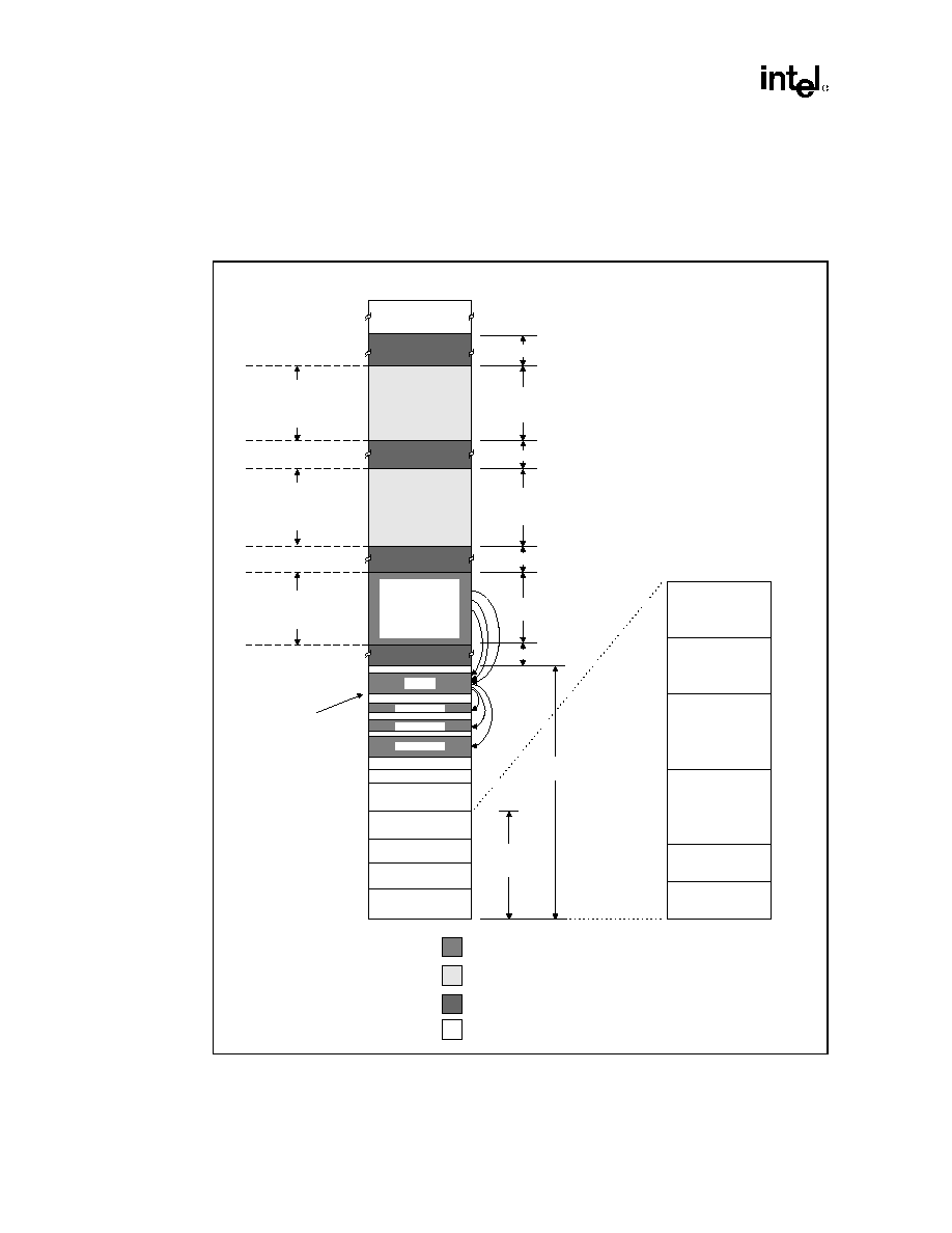
Functional Description
4-2
82443GX Host Bridge Datasheet
4.1.1
Memory Address Ranges
Figure 4-1 provides a detailed 82443GX memory map indicating specific memory regions defined
by AGP and supported by the Intel
Æ
440GX AGPset.
Figure 4-1. Memory System Address Space
mem_map2.vsd
Notes:
1. Graphics Device accesses to the AGP aperture
invoke AGP transfer protocol on the AGP Bus
and use GART to re- map the accesses to
graphics data structures located in main
memory.
2. The two window regions provide PCI accesses
over the AGP.
Main memory (physical memory) and
CPU extended memory (above 4 GB)
PCI memory accesses to primary PCI bus
AGP aperture, GART, and
Graphics data structures mapped by GART
PCI memory accesses to AGP
4 GB
System Memory Space
TOM (2 GB Max.)
Main
Memory
Local Graphics Memory
- Frame Buffer
- Rendering Buffer
- Depth Buffer (Z)
- Video Capture Buffer
Window For Prefetchable
PCI accesses to AGP
(Base=PMBASE Reg. (24h); Dev 1)
(Size=PMLIMIT Reg. (26h); Dev 1)
Graphics Address Re-Mapping Table
(Base=ATTBASE Reg. (B8h); Dev 0)
Window For Non-Prefetchable
PCI accesses to AGP
(Base=MBASE Reg. (20h); Dev 0)
(Size=MLIMIT Reg. (22h); Dev 0)
64 GB
Extended CPU
Memory Space
PCI Memory
PCI Memory
accesses to AGP
PCI Memory
accesses to AGP
PCI Memory
PCI Memory
Graphics Device
Access
(e.g., memory-mapped
control/status registers)
GART
AGP
Aperture
PCI Memory
AGP Data
AGP Data
AGP Data
AGP Aperture
- Textures
- Other Surfaces
- Instruction
Stream
00000h
A0000h
BFFFFh
System/Application SW
Graphics Adapter
(128 KB)
C0000h
Video BIOS
(shadowed in memory)
0FFFFFh
DOS
Compatibility
Memory
1 MB
Optional ISA Hole
15 MB
16 MB
Upper BIOS Area
(64 KB)
Lower BIOS Area
(64 KB)
16KBx4
Expansion Card BIOS
and Buffer Area
(128 KB) 16KBx8
Standard PCI/ISA Video
Memory (SMM Mem)
128 KB
Optional Fixed Memory
Hole
DOS Area
(512 KB)
000000h
080000h
07FFFFh
0A0000h
09FFFFh
0C0000h
0BFFFFh
0E0000h
0DFFFFh
0F0000h
0EFFFFh
0FFFFFh
1 MB
960 KB
896 KB
768 KB
640 KB
512 KB
0 KB
AGP Aperture Range
(Base=APBASE Reg. (10h); Dev 0)
(Size=APSIZE Reg. (B4h); Dev 0)

82443GX Host Bridge Datasheet
4-3
Functional Description
4.1.1.1
Compatibility Area
This area is divided into the following address regions:
∑
0≠512 KB DOS Area
∑
512 KB ≠ 640 KB DOS Area - Optional ISA/PCI Memory
∑
640KB ≠ 768 KB Video Buffer Area
∑
768 KB ≠ 896 KB in 16KB sections (total of 8 sections) - Expansion Area
∑
896KB ≠ 960 KB in 16KB sections (total of 4 sections) - Extended System BIOS Area
∑
960 KB ≠ 1 MB Memory (BIOS Area) - System BIOS Area
There are sixteen memory segments in the compatibility area. Thirteen of the memory ranges can
be enabled or disabled independently for both read and write cycles. One segment
(512 KB≠640 KB) which can be mapped to either main DRAM or PCI.
DOS Area (00000h≠9FFFh)
The DOS area is 640 KB and it is further divided into two parts. The 512 KB area at 0 to 7FFFFh is
always mapped to the main memory controlled by the 82443GX, while the 128 KB address range
from 080000 to 09FFFFh can be mapped to PCI or to main DRAM. By default this range is
mapped to main memory and can be declared as a main memory hole (accesses forwarded to PCI)
via the 82443GX's FDHC configuration register.
Video Buffer Area (A0000h≠BFFFFh)
The 128 KB graphics adapter memory region is normally mapped to a legacy video device on PCI
(typically VGA controller). This area is not controlled by attribute bits and CPU-initiated cycles in
this region are forwarded to PCI or AGP for termination. This region is also the default region for
SMM space.
The SMRAM Control register controls how SMM accesses to this space are treated.
Table 4-1. Memory Segments and their Attributes
Memory Segments
Attributes
Comments
000000h≠07FFFFh
fixed - always mapped to main DRAM
0 ≠ 512 KB; DOS Region
080000h≠09FFFFh
configurable as PCI or main DRAM
512 KB ≠ 640 KB; DOS Region
0A0000h≠0BFFFFh
mapped to PCI - configurable as SMM
space
Video Buffer (physical DRAM
configurable as SMM space)
0C0000h≠0C3FFFh
WE; RE
Add-on BIOS
0C4000h≠0C7FFFh
WE; RE
Add-on BIOS
0C8000h≠0CBFFFh
WE; RE
Add-on BIOS
0CC000h≠0CFFFFh
WE; RE
Add-on BIOS
0D0000h≠0D3FFFh
WE; RE
Add-on BIOS
0D4000h≠0D7FFFh
WE; RE
Add-on BIOS
0D8000h≠0DBFFFh
WE; RE
Add-on BIOS
0DC000h≠0DFFFFh
WE; RE
Add-on BIOS
0E0000h≠0E3FFFh
WE; RE
BIOS Extension
0E4000h≠0E7FFFh
WE; RE
BIOS Extension
0E8000h≠0EBFFFh
WE; RE
BIOS Extension
0EC000h≠0EFFFFh
WE; RE
BIOS Extension
0F0000h≠0FFFFFh
WE; RE
BIOS Area

Functional Description
4-4
82443GX Host Bridge Datasheet
Monochrome Adapter (MDA) Range (B0000h≠B7FFFh)
Legacy support requires the ability to have a second graphics controller (monochrome) in the
system. In an AGP system, accesses in the normal VGA range are forwarded to the AGP bus. Since
the monochrome adapter may be on the PCI (or ISA) bus, the 82443GX must decode cycles in the
MDA range and forward them to PCI.
Expansion Area (C0000h≠DFFFFh)
This 128 KB ISA Expansion region is divided into eight 16 KB segments. Each segment can be
assigned one of four Read/Write states: read-only, write-only, read/write, or disabled. Typically,
these blocks are mapped through the Host-to-PCI bridge and are subtractively decoded to ISA
space. Memory that is disabled is not remapped.
Extended System BIOS Area (E0000h≠EFFFFh)
This 64 KB area is divided into four 16 KB segments. Each segment can be assigned independent
read and write attributes so it can be mapped either to main DRAM or to PCI. Typically, this area is
used for RAM or ROM. Memory segments that are disabled are not remapped elsewhere.
System BIOS Area (F0000h≠FFFFFh)
This area is a single 64 KB segment. This segment can be assigned read and write attributes. It is by
default (after reset) Read/Write disabled and cycles are forwarded to PCI. By manipulating the
Read/Write attributes, the 82443GX can "shadow" BIOS into the main DRAM. When disabled,
this segment is not remapped.
4.1.1.2
Extended Memory Area
This memory area covers 100000h (1 MB) to FFFFFFFFh (4 GB-1) address range and it is divided
into the following regions:
∑
Main DRAM Memory from 1 MB to the Top of Memory
∑
PCI Memory space from the Top of Memory to 4 GB with two specific ranges:
-- APIC Configuration Space from FEC0_0000h (4 GB-20 MB) to FECF_FFFFh and
EE0_0000h to FEEF_FFFFh
-- High BIOS area from 4 GB to 4 GB ≠ 2 MB
Main DRAM Address Range (0010_0000h to Top of Main Memory)
The address range from 1 MB to the top of main memory is mapped to main DRAM address range
controlled by the 82443GX. All accesses to addresses within this range will be forwarded by the
82443GX to the DRAM unless a hole in this range is created using the fixed hole as controlled by
the FDHC register. Accesses within this hole are forwarded to PCI.
The range of physical DRAM memory disabled by opening the hole is not remapped to the Top of
the Memory.
Extended SMRAM Address Range (Top of Main Memory ≠ TSEG)
An extended SMRAM space of up to 1 MB can be defined in the address range at the top of
memory. The size of the SMRAM space is determined by the TSEG value in the ESMRAMC
register. When the extended SMRAM space is enabled, non-SMM CPU accesses and all PCI and

82443GX Host Bridge Datasheet
4-5
Functional Description
AGP accesses in this range are forwarded to PCI. When SMM is enabled the amount of memory
available to the system is equal to the amount of physical DRAM minus the value in the TSEG
register.
Note:
When extended SMRAM is used, the maximum amount of DRAM supported is limited to 256 MB.
PCI Memory Address Range (Top of Main Memory to 4 GB)
The address range from the top of main DRAM to 4 GB (top of physical memory space supported
by the Intel
Æ
440GX AGPset) is normally mapped to PCI. There are two exceptions to this rule:
∑
Addresses decoded to the AGP Memory Window defined by the MBASE, MLIMIT,
PMBASE, and PMLIMIT registers are mapped to AGP.
∑
Addresses decoded to the Graphics Aperture range defined by the APBASE and APSIZE
registers are mapped to the main DRAM.
There are two sub-ranges within the PCI Memory address range defined as APIC Configuration
Space and High BIOS Address Range. The AGP Memory Window and Graphics Aperture Window
MUST NOT overlap with these two ranges. These ranges are described in detail in the following
paragraphs.
APIC Configuration Space (FEC0_0000h -FECF_FFFFh, FEE0_0000h- FEEF_FFFFh)
This range is reserved for APIC configuration space which includes the default I/O APIC
configuration space. The default Local APIC configuration space is FEE0_0000h to FEEF_0FFFh.
CPU accesses to the Local APIC configuration space do not result in external bus activity since the
Local APIC configuration space is internal to the CPU. However, a MTRR must be programmed to
make the Local APIC range uncacheable (UC). The Local APIC base address in each CPU should
be relocated to the FEC0_0000h (4 GB ≠ 20 MB) to FECF_FFFFh range so that one MTRR can be
programmed to 64 KB for the Local and I/O APICs. The I/O APIC(s) usually reside in the I/O
Bridge portion of the AGPset or as a stand-alone component(s). For Intel
Æ
440GX AGPset systems
using the PIIX4E, the I/O APIC is supported as a stand-alone component residing on the X-Bus.
I/O APIC units will be located beginning at the default address FEC0_0000h. The first I/O APIC
will be located at FEC0_0000h. Each I/O APIC unit is located at FEC0_x000h where x is I/O APIC
unit number 0 through F (hex). This address range will be normally mapped to PCI.
Note:
There is no provision to support an I/O APIC device on AGP.
The address range between the APIC configuration space and the High BIOS (FED0_0000h to
FEDF_FFFFh) is always mapped to the PCI.
High BIOS Area (FFE0_0000h ≠FFFF_FFFFh)
The top 2 MB of the Extended Memory Region is reserved for System BIOS (High BIOS),
extended BIOS for PCI devices, and the A20 alias of the system BIOS. CPU begins execution from
the High BIOS after reset. This region is mapped to PCI so that the upper subset of this region
aliases to 16 MB≠256 KB range. The actual address space required for the BIOS is less than 2 MB
but the minimum CPU MTRR range for this region is 2 MB so that full 2 MB must be considered.
The PIIX4E supports a maximum of 1 MB in the High BIOS range.

Functional Description
4-6
82443GX Host Bridge Datasheet
4.1.1.3
AGP Memory Address Range
The 82443GX can be programmed to direct memory accesses to the AGP bus interface when
addresses are within either of two ranges specified via registers in 82443GX Device #1
configuration space. The first range is controlled via the Memory Base Register (MBASE) and
Memory Limit Register (MLIMIT) registers. The second range is controlled via the Prefetchable
Memory Base (PMBASE) and Prefetchable Memory Limit (PMLIMIT) registers
The 82443GX positively decodes memory accesses to AGP memory address space as defined by
the following equations:
Memory_Base_Address
Address
Memory_Limit_Address
Prefetchable_Memory_Base_Address
Address
Prefetchable_Memory_Limit_Address
The effective size of the range is programmed by the plug-and-play configuration software and it
depends on the size of memory claimed by the AGP compliant device. Normally, these ranges
reside above the Top-of-Main-DRAM and below High BIOS and APIC address ranges.
Note:
The 82443GX Device #1 memory range registers described above are used to allocate memory
address space for any devices on AGP that require such a window. These devices include the AGP
compliant device, and multifunctional AGP compliant devices where one or more functions are
implemented as PCI devices.
4.1.1.4
AGP DRAM Graphics Aperture
Memory-mapped, graphics data structures can reside in a Graphics Aperture to main DRAM
memory. This aperture is an address range defined by the APBASE configuration register of the
82443GX Host Bridge. The APBASE register follows the normal base address register template as
defined by the PCI 2.1 specification. The size of the range claimed by the APBASE is programmed
via "back-end" register APSIZE (programmed by the chip-set specific BIOS before plug-and-play
session is performed). APSIZE allows selection of the aperture size of 4 MB, 8 MB,16 MB,
32 MB, 64 MB, 128 MB and 256 MB. By programming APSIZE to a specific size, the
corresponding lower bits of APBASE are forced to "0" (behave as hardwired). Default value of
APSIZE forces aperture size of 256 MB. Aperture address range is naturally aligned.
Although this aperture appears to be established in PCI memory space, in fact the 82443GX
forwards accesses within the aperture range to the main DRAM subsystem. The originally issued
addresses are translated (within 82443GX's DRAM controller subsystem) via a translation table
maintained in main memory. Translation table entries may be partially cached in a Graphics
Translation Look-aside Buffer (GTLB) implemented within the 82443GX's DRAM subsystem.
The aperture range will not be cacheable in the processor caches.
4.1.1.5
System Management Mode (SMM) Memory Range
82443GX supports the use of main memory as System Management RAM (SMRAM) enabling the
use of System Management Mode. The 82443GX supports two SMRAM options: Compatible
SMRAM (C_SMRAM) and Extended SMRAM (E_SMRAM). System Management RAM
(SMRAM) space provides a memory area that is available for the SMI handler's and code and data
storage. This memory resource is normally hidden from the system OS so that the processor has
immediate access to this memory space upon entry to SMM. The 82443GX provides three
SMRAM options:

82443GX Host Bridge Datasheet
4-7
Functional Description
∑
Below 1 MB option that supports compatible SMI handlers.
∑
Above 1 MB option that allows new SMI handlers to execute with write-back cacheable
SMRAM.
∑
Optional larger write-back cacheable T_SEG area from 128KB to 1MB in size above 1 MB
that is reserved from the highest area in system DRAM memory. The above 1 MB solutions
require changes to compatible SMRAM handlers code to properly execute above 1 MB.
Table 4-2 summarizes the operation of SMRAM space cycles targeting the SMI space addresses.
NOTE:
1.
1 = Enabled and 0 = Disabled
Table 4-4 defines the control of the decode for all code fetches and data fetches to SMRAM ranges
(as defined by Table 4-3). The G_SMRAM bit provides a global disable for all SMRAM memory.
The D_OPEN bit allows software to write to the SMRAM ranges without being in SMM. BIOS
software can use this bit to initialize SMM code at Power up. The D_LCK bit limits the SMRAM
range access to only SMM mode accesses. The D_CLS bit causes SMM data accesses to be
forwarded to PCI. The SMM software can use this bit to write to video memory while running code
out of DRAM.
NOTE:
1.
1 = Enabled and 0 = Disabled
Table 4-2. SMRAM Decoding
Name of Range
Transaction Address
DRAM Address
compatible (Range A)
A0000≠BFFFFh
A0000≠BFFFFh
HI-SMRAM (RANGE H)
256M + A0000h to 256M + FFFFFh
A0000≠FFFFFh
TSEG (RANGE T)
256M + TOM to 256M + TOM - TSEG_SIZE
TOM to TOM - TSEG_SIZE
Table 4-3. SMRAM Range Decode
Global SMRAM
H_SMRAME
TSEG_EN
A Range
H Range
T Range
0
x
x
Disable
Disable
Disable
1
0
0
Enable
Disable
Disable
1
0
1
Enable
Disable
Enable
1
1
0
Disabled
Enable
Disable
1
1
1
Disabled
Enable
Enable
Table 4-4. SMRAM Decode Control
G_SMRAME
D_LCK
D_CLS
D_OPEN
SMM Mode
SMM Code
Fetch
SMM Data
Fetch
0
x
x
x
x
Disable
Disable
1
0
x
0
0
Disable
Disable
1
0
0
0
1
Enable
Enable
1
0
0
1
x
Enable
Enable
1
0
1
0
1
Enable
Disable
1
0
1
1
x
Invalid
Invalid
1
1
x
x
0
Disable
Disable
1
1
0
x
1
Enable
Enable
1
1
1
x
1
Enable
Disable

Functional Description
4-8
82443GX Host Bridge Datasheet
Refer to Section 4.8, "Power Management" on page 4-23 for more details on SMRAM support.
Reiteration:
∑
Only un-cacheable SMM regions may overlap PCI or AGP Windows.
∑
SMM regions will not overlap the AGP aperture.
∑
Software (not in SMM) will not access PCI memory behind cacheable SMM regions.
∑
PCI or AGP masters cannot access the SMM space.
4.1.2
Memory Shadowing
Any block of memory that can be designated as read-only or write-only can be "shadowed" into
82443GX DRAM memory. Typically, this is done to allow ROM code to execute more rapidly out
of main DRAM. ROM is used as a read-only during the copy process while DRAM at the same
time is designated write-only. After copying, the DRAM is designated read-only so that ROM is
shadowed. CPU bus transactions are routed accordingly.
4.1.3
I/O Address Space
The 82443GX does not support the existence of any other I/O devices besides itself on the CPU
bus. The 82443GX generates either PCI or AGP bus cycles for all CPU I/O accesses. The
82443GX contains three internal registers in the CPU I/O space, Configuration Address Register
(CONFIG_ADDRESS) and the Configuration Data Register (CONFIG_DATA) and Power
Management Control Register. These locations are used to implement PCI configuration space
access mechanism and as described in Section 3.1, "I/O Mapped Registers" on page 3-2.
The CPU allows 64K+3 bytes to be addressed within the I/O space. The 82443GX propagates the
CPU I/O address without any translation on to the destination bus and therefore provides
addressability for 64K+3 byte locations. Note that the upper 3 locations can be accessed only
during I/O address wrap-around when CPU bus A16# address signal is asserted. A16# is asserted
on the CPU bus whenever an I/O access is made to 4 bytes from address 0FFFDh, 0FFFEh, or
0FFFFh. A16# is also asserted when an I/O access is made to 2 bytes from address 0FFFFh.
The I/O accesses (other than ones used for PCI configuration space access) are forwarded normally
to the PCI bus unless they fall within the PCI1/AGP I/O address range as defined by the
mechanisms in Section 4.1.4. The 82443GX will not post I/O write cycles to IDE.
4.1.4
AGP I/O Address Mapping
The 82443GX can be programmed to direct non-memory (I/O) accesses to the AGP bus interface
when CPU-initiated I/O cycle addresses are within the AGP I/O address range. This range is
controlled via the I/O Base Address (IOBASE) and I/O Limit Address (IOLIMIT) registers in
82443GX Device #1 configuration space.
The 82443GX positively decodes I/O accesses to AGP I/O address space as defined by the
following equation:
I/O_Base_Address
CPU I/O Cycle Address
I/O_Limit_Address
The effective size of the range is programmed by the plug-and-play configuration software and it
depends on the size of I/O space claimed by the AGP compliant device.

82443GX Host Bridge Datasheet
4-9
Functional Description
Note that the 82443GX Device #1 I/O address range registers defined above are used for all I/O
space allocation for any devices requiring such a window on AGP. These devices would include the
AGP compliant device and multifunctional AGP compliant devices where one or more functions
are implemented as PCI devices.
4.1.5
Decode Rules and Cross-Bridge Address Mapping
The address map described above applies globally to accesses arriving on any of the three
interfaces (i.e., Host bus, PCI or AGP).
4.1.5.1
PCI Interface Decode Rules
The 82443GX accepts accesses from PCI to the following address ranges:
∑
All memory read and write accesses to Main DRAM
∑
Memory Write accesses to AGP memory range defined by MBASE, MLIMIT, PMBASE, and
PMLIMIT. 82443GX will not respond to memory read accesses to this range.
∑
Memory read/write accesses to the Graphics Aperture defined by APBASE and APSIZE.
PCI accesses that fall elsewhere within the PCI memory range will not be accepted. PCI cycles not
explicitly claimed by the 82443GX are either subtractively decoded or master-aborted on PCI.
4.1.5.2
AGP Interface Decode Rules
Cycles Initiated Using PCI Protocol
Accesses between AGP and PCI are limited to memory writes using the PCI protocol. Write cycles
are forwarded to PCI if the addresses are not within main DRAM range, AGP memory ranges, or
Graphics Aperture range.
The 82443GX will claim AGP initiated memory read transactions decoded to the main DRAM
range or the Graphics Aperture range. All other memory read requests will be master-aborted by
the AGP initiator as a consequence of 82443GX not responding to a transaction.
If agent on AGP issues an I/O, PCI Configuration or PCI Special Cycle transaction, the 82443GX
will not respond and cycle will result in a master-abort.
Cycles Initiated Using AGP Protocol
All cycles must reference main memory (i.e., main DRAM address range or Graphics Aperture
range which is also physically mapped within DRAM but using different address range).
AGP-initiated cycles that target DRAM are not snooped on the host bus, even if they fall outside of
the AGP aperture range.
If cycle is outside of main memory range then it will terminate as follows:
∑
Reads: return random value
∑
Writes: dropped "on the floor" i.e. terminated internally without affecting any buffers or main
memory
∑
ECC errors that occur on reads outside of DRAM are not reported or scrubbed.

Functional Description
4-10
82443GX Host Bridge Datasheet
4.1.5.3
Legacy VGA Ranges
The legacy VGA memory range A0000h≠BFFFFh is mapped either to PCI or to AGP depending on
the programming of the BCTRL configuration register in 82443GX Device #1 configuration space,
and the NBXCONF (MDAP bit) configuration register in Device #0 configuration space. The same
registers control mapping of VGA I/O address ranges. VGA I/O range is defined as addresses
where A[9:0] are in the ranges 3B0h to 3BBh and 3C0h to 3DFh (inclusive of ISA address aliases -
A[15:10] are not decoded).
4.2
Host Interface
The host interface of the 82443GX is optimized to support the Pentium II and Pentium II XeonTM
processors with bus clock frequencies of 100 MHz. The 82443GX implements the host address,
control, and data bus interfaces within a single device. Host bus addresses are decoded by the
82443GX for accesses to main memory, PCI memory, PCI I/O, PCI configuration space and AGP
space (memory, I/O and configuration). The 82443GX takes advantage of the pipelined addressing
capability of the Pentium II processor to improve the overall system performance.
4.2.1
Host Bus Device Support
The 82443GX recognizes and supports a large subset of the transaction types that are defined for
the Pentium Pro processor bus interface. However, each of these transaction types have a multitude
of response types, some of which are not supported by this controller. All transactions are
processed in the order that they are received on the Pentium
Æ
Pro processor bus. Table 4-5
summarizes the transactions supported by the 82443GX.
Topic
Definition
AGP IO
range
The AGP bus can be allocated with 1 block of IO space with a granularity of 4KB. The IO base
address register points to the beginning of the AGP IO range while IO limit address register
points to the end of this range. The IO range definition is based on the PCI to PCI specification.
ISA_EN
The ISA_EN bit in the 82443GX device1 is necessary in ISA bus based systems where there is
a need to allocate IO space to AGP bus devices. This is necessary since legacy ISA devices
decode IO range of address [9:0] only and thus the IO address of the devices are aliased for
every 1 KB of the 64 KB IO range. Therefore, to provide IO range to AGP bus and maintain the
ISA IO legacy rules, the ISA_EN is set. As a result, all CPU cycles in the address ranges:
"xxxx_xx01_0000_0000"b to "xxxx_xx11_1111_1111"b, that is the top 768 bytes of each 1KB
aligned block, are sent to the PCI bus independent of whether this particular address is inside or
outside the range allocated to the AGP bus.
The above is relevant only to CPU-initiated cycles, as PCI and AGP master IO cycles are never
claimed by the 82443GX. The ISA_EN functional definition is based on the PCI to PCI
specification.
VGA_EN
VGA IO range is defined in the following ranges: 3B0-3BBh, 3C0-3DFh. When the VGA_EN is
set, all CPU initiated IO cycles in the VGA IO range are forwarded to the AGP bus, independent
of whether the ISA_EN bit is set or not. Thus the VGA_EN bit setting takes precedence relative
to the setting of the ISA_EN bit. The VGA_EN functional definition is based on the PCI to PCI
specification.
MDAP
The MDA IO range includes the ports 3B4h, 3B5h, 3B8h, 3B9h, 3BAh, 3BFh. Once the VGA_EN
is set, it is legal to set the MDAP bit to indicate that a second CRT controller (Monochrome
Display Adapter) resides in the PCI or ISA bus. In this case, all the CPU-initiated IO cycles in the
VGA range that are not in to the above ports are sent to AGP bus while the cycles to the above
six IO ports (and to all the aliased ports) are sent to PCI bus.
Note that the CPU IO cycles to the above ports are sent to AGP bus independent of the AGP IO
range and ISA_EN setting.

82443GX Host Bridge Datasheet
4-11
Functional Description
NOTE:
1. For Memory cycles, REQa[4:3]# = ASZ#. The 82443GX only supports ASZ# = 00 (32 bit address).
2. REQb[4:3]# = DSZ#. For the Pentium
Æ
Pro processor, DSZ# = 00 (64 bit data bus size).
3. LEN# = data transfer length as follows:
LEN#
Data length
00
8 bytes (BE[7:0]# specify granularity)
01
Length = 16 bytes BE[7:0]# all active
10
Length = 32 bytes BE[7:0]# all active
11
Reserved
Table 4-5. Host Bus Transactions Supported By 82443GX
Transaction
REQA[4:0]#
REQB[4:0]#
82443GX Support
Deferred Reply
0 0 0 0 0
X X X X X
The 82443GX initiates a deferred reply for a
previously deferred transaction.
Reserved
0 0 0 0 1
X X X X X
Reserved
Interrupt Acknowledge
0 1 0 0 0
0 0 0 0 0
Interrupt acknowledge cycles are forwarded to
the PCI bus.
Special Transactions
0 1 0 0 0
0 0 0 0 1
See separate table in Special Cycles section.
Reserved
0 1 0 0 0
0 0 0 1 x
Reserved
Reserved
0 1 0 0 0
0 0 1 x x
Reserved
Branch Trace Message
0 1 0 0 1
0 0 0 0 0
The 82443GX terminates a branch trace
message without latching data.
Reserved
0 1 0 0 1
0 0 0 0 1
Reserved
Reserved
0 1 0 0 1
0 0 0 1 x
Reserved
Reserved
0 1 0 0 1
0 0 1 x x
Reserved
I/O Read
1 0 0 0 0
0 0 x LEN#
I/O read cycles are forwarded to PCI or AGP.
I/O cycles which are in the 82443GX
configuration space are not forwarded to PCI.
I/O Write
1 0 0 0 1
0 0 x LEN#
I/O write cycles are forwarded to PCI or AGP.
I/O cycles which are in the 82443GX
configuration space are not forwarded to PCI.
Reserved
1 1 0 0 x
0 0 x x x
Reserved
Memory Read &
Invalidate
0 0 0 1 0
0 0 x LEN#
Host initiated memory read cycles are
forwarded to DRAM or the PCI/1 bus. The
82443GX initiates an MRI cycle for a PCI/1
initiated write cycle to DRAM.
Reserved
0 0 0 1 1
0 0 x LEN#
Reserved
Memory Code Read
0 0 1 0 0
0 0 x LEN#
Memory code read cycles are forwarded to
DRAM or PCI/1.
Memory Data Read
0 0 1 1 0
0 0 x LEN#
Host initiated memory read cycles are
forwarded to DRAM or the PCI/1 bus. The
82443GX initiates a memory read cycle for a
PCI/1 initiated read cycle to DRAM.
Memory Write (no retry)
0 0 1 0 1
0 0 x LEN#
This memory write is a writeback cycle and
cannot be retried. The 82443GX forwards the
write to DRAM.
Memory Write (can be
retried)
0 0 1 1 1
0 0 x LEN#
The normal memory write cycle is forwarded
to DRAM or PCI/1.
Functional Description
4-12
82443GX Host Bridge Datasheet
Special Cycles
A Special Cycle is defined when REQa[4:0] = 01000 and REQb[4:0]= xx001. The first address
phase Aa[35:3]# is undefined and can be driven to any value. The second address phase, Ab[15:8]#
defines the type of Special Cycle issued by the processor.
Table 4-3 specifies the cycle type and definition as well as the action taken by the 82443GX when
the corresponding cycles are identified.
Table 4-6. Host Responses supported by the 82443GX
RS2#
RS1#
RS0#
Description
82443GX Support
0
0
0
idle
0
0
1
Retry Response
To avoid deadlock, this response is generated when a
resource cannot currently be accessed by the
processor. PCI-directed reads, writes, DRAM locked
reads, AGP reads and writes can be retried.
0
1
0
Deferred Response
This response can be returned for all transactions that
can be executed `out of order.' PCI-directed reads
(memory, I/O and Interrupt Acknowledge) and writes
(I/O only), and AGP directed reads (memory and I/O)
and writes (I/O only) can be deferred.
0
1
1
Reserved
Reserved
1
0
0
Hard Failure
Not supported.
1
0
1
No Data Response
This is for transactions where the data has already
been transferred or for transactions where no data is
transferred. Writes and zero length reads receive this
response.
1
1
0
Implicit Writeback
This response is given for those transactions where
the initial transactions snoop hits on a modified cache
line.
1
1
1
Normal Data
Response
This response is for transactions where data
accompanies the response phase. Reads receive this
response.
Table 4-7. Host Special Cycles with 82443GX
BE[7:0}#
Special
Cycle Type
Action Taken
0000
0000
NOP
This transaction has no side-effects.
0000
0001
Shutdown
This transaction is issued when an agent detects a severe software error that
prevents further processing. This cycle is claimed by the 82443GX. The
82443GX issues a shutdown special cycle on the PCI bus. This cycle is retired on
the CPU bus after it is terminated on the PCI via a master abort mechanism.
0000
0010
Flush
This transaction is issued when an agent has invalidated its internal caches
without writing back any modified lines. The 82443GX claims this cycle and
retires it.
0000
0011
Halt
This transaction is issued when an agent executes a HLT instruction and stops
program execution. This cycle is claimed by the 82443GX and propagated to PCI
as a Special Halt Cycle. This cycle is retired on the CPU bus after it is terminated
on the PCI via a master abort mechanism.
0000
0100
Sync
This transaction is issued when an agent has written back all modified lines and
has invalidated its internal caches. The 82443GX claims this cycle and retires it.
82443GX Host Bridge Datasheet
4-13
Functional Description
NOTE:
1. None of the host bus special cycles is propagated to the AGP interface.
4.2.2
Symmetric Multiprocessor (SMP) Protocol Support
The Intel
Æ
440GX AGPset is optimized for uniprocessor system and also supports the symmetrical
multiprocessor configurations of up to two CPUs on the host bus.
When configured for dual-processor, the Intel
Æ
440GX AGPset-based platform must integrate an
I/O APIC functionality and WSC# signaling mechanism must be enabled.
4.2.3
In-Order Queue Pipelining
The 82443GX interface to the CPU bus includes a four deep in-order queue to track pipelined bus
transactions.
4.2.4
Frame Buffer Memory Support (USWC)
To allow for high speed write capability for graphics, the Pentium Pro processor family has
introduced USWC memory type. The USWC (uncacheable, speculative, write-combining) memory
type provides a write-combining buffering mechanism for write operations. A high percentage of
graphics transactions are writes to the memory-mapped graphics region, normally known as the
linear frame buffer. Reads and writes to USWC are non-cached and can have no side effects.
In the case of graphics, current 32-bit drivers (without modifications) would use Partial Write
protocol to update the frame buffer. The highest performance write transaction on the CPU bus is
the Line Write.
0000
0101
Flush
Acknowledge
This transaction is issued when an agent has completed a cache sync and flush
operation in response to an earlier FLUSH# signal assertion. The 82443GX
claims this cycle and retires it.
0000
0110
Stop Clock
Acknowledge
This transaction is issued when an agent enters Stop Clock mode. This cycle is
claimed by the 82443GX and propagated to the PCI as a Special Stop Grant
Cycle. This cycle is completed on the CPU bus after it is terminated on the PCI
via a master abort mechanism.
0000
0111
SMI
Acknowledge
This transaction is first issued when an agent enters the System Management
Mode (SMM).
all others
Reserved
Table 4-7. Host Special Cycles with 82443GX
BE[7:0}#
Special
Cycle Type
Action Taken

Functional Description
4-14
82443GX Host Bridge Datasheet
4 . 3
D R A M I n t e r f a c e
The 82443GX integrates a main memory DRAM controller that supports a 64-bit or 72-bit (64-bit
memory data plus 8 ECC) DRAM array. The DRAM type supported is Synchronous (SDRAM).
The 82443GX does not support mixing of SDRAM and Registered SDRAM. The 82443GX
DRAM interface runs at 100 MHz. The DRAM controller interface is fully configurable through a
set of control registers. Complete descriptions of these registers are given in the Register Section. A
brief overview of the registers which configure the DRAM interface is provided in this section.
The fifteen multiplexed address lines, MA[14:0], allow the 82443GX to support 2M, 4M, 8M,
16M, 32M, and 64M x72/64 DIMMs. Asymmetric addressing is supported. The 82443GX has
sixteen CS# lines, used in pairs enabling the support of up to eight 64/72-bit rows of DRAM. For
write operations of less than a QWord in size, the 82443GX will either perform a byte-wise write
(non-ECC protected configuration) or a read-modify-write cycle by merging the write data on a
byte basis with the previously read data (ECC or EC configurations). The 82443GX targets
SDRAM with CL2 and CL3 and supports both single and double-sided DIMMs. The 82443GX
provides refresh functionality with programmable rate (normal DRAM rate is 1 refresh/15.6ms).
The 82443GX can be configured via the Paging Policy Register to keep multiple pages open within
the memory array. Pages can be kept open in all rows of memory. When 4 bank SDRAM devices
are used for a particular row, up to 4 pages can be kept open within that row.
The DRAM interface of the 82443GX is configured by the DRAM Control Register, DRAM
Timing Register, SDRAM Control Register, bits in the NBXCFG and the eight DRAM Row
Boundary (DRB) Registers. The DRAM configuration registers noted above control the DRAM
interface to select SDRAM or registered SDRAM, RAS timings, and CAS rates. The eight DRB
Registers define the size of each row in the memory array, enabling the 82443GX to assert the
proper CSA/B# pair for accesses to the array.
4.3.1
DRAM Organization and Configuration
The 82443GX supports 64/72-bit DRAM configurations. In the following discussion the term row
refers to a set of memory devices that are simultaneously selected by a CSA/B# pair. A row may be
composed of discrete DRAM devices, single-sided or double-sided DIMMs.
The 82443GX has multiple copies of many of the signals interfacing to memory. The interface
consists of the following pins.
∑
Multiple copies
-- MAA[14:0], MAB[12:11,9:0]# and MAB[14,13,10]
-- CSA[7:0]#, CSB[7:0]#
-- SRASA#, SRASB#
-- SCASA#, SCASB#
-- WEA#, WEB#
-- DQMA[7:0], DQMB[5,1]
∑
Single Copy
-- MD[63:0]
-- MECC[7:0]
-- GCKE
-- FENA (FET switch control for 4 DIMM configurations designed with FETs)
Two CS# lines are provided per row. These are functionally equivalent. The extra copy is provided
for loading reasons. The two SRAS#'s, SCAS#'s and WE#'s are also functionally equivalent and
each copy drives two rows of DRAM. Most pins utilize programmable strength output buffers
82443GX Host Bridge Datasheet
4-15
Functional Description
(refer to Register Section). When a row contains 16Mb SDRAMs, MAA11 and MAB11 function
as Bank Select lines. When a row contains 64Mb, 128Mb, or 256Mb
1
SDRAMs, MAA/B[12:11]
function as Bank Addresses (BA[1:0], or Bank Selects).
The entire memory array may be configured as either unbuffered SDRAM or registered SDRAM.
Mixing DRAM types within one system is not supported. DIMMs may be populated in any order.
That is, any combination of rows may be populated. Registered SDRAM DIMMs allow for support
of x4 SDRAM components.
Figure 4-2 depicts the 82443GX connections for an SDRAM memory array and shows how the
copies of the signals are distributed to the array. If cross bar switches are used, the unused input
must be pulled down through a resistor. GCKE requires external logic (not shown).
1.
Proper operation of the 82443GX AGPset with 256-Mbit SDRAM devices has not yet been verified. Intel's current plans are to validate this feature
in the second half of 1998 when 256-Mbit SDRAM devices are available.
Figure 4-2. Four-DIMM Configuration with FET switches
CSA[7:6]#, CSB[7:6]#
CSA[5:4]#, CSB[5:4]#
CSA[3:2]#, CSB[3:2]#
CSA[1:0]#, CSB[1:0]#
SRASA#
SRASB#
SCASA#
SCASB#
DQMA[1,5]
DQMA[7,6,4:2,0]
DQMB[1,5]
WEA#
WEB#
GCKE
MAA[14:0]
MAB[14,13:11#, 10, 9:0#]
MD[63:0]
FENA
MECC[7:0]
DIMM_CLK[3:0]
DIMM_CLK[7:4]
DIMM_CLK[11:8]
DIMM_CLK[15:12]
SMB_CLK
SMB_DATA
Mux
Mux
Shift
Register
Group 0
RGCKE[7:0]#
Group 1

Functional Description
4-16
82443GX Host Bridge Datasheet
4.3.1.1
Configuration Mechanism For DIMMS
Detection of the type of DRAM installed on the DIMM is supported via Serial Presence Detect
mechanism as defined in the JEDEC 168-pin DIMM standard. This standard uses the SCL, SDA
and SA[2:0] pins on the DIMMs to detect the type and size of the installed DIMMs. No special
programmable modes are provided on the 82443GX for detecting the size and type of memory
installed. Type and size detection must be done via the serial presence detection pins.
Memory Detection and Initialization
Before any cycles to the memory interface can be supported, the 82443GX DRAM registers must
be initialized. The 82443GX must be configured for operation with the installed memory types.
Detection of memory type and size is done via the System Management Bus (SMB) interface on
the PIIX4E. This two wire bus is used to extract the DRAM type and size information from the
serial presence detect port on the DRAM DIMMs.
DRAM DIMMs contain a 5 pin serial presence detect interface, including SCL (serial clock), SDA
(serial data) and SA[2:0]. Devices on the SMBus bus have a seven bit address. For the DRAM
DIMMs, the upper four bits are fixed at 1010. The lower three bits are strapped on the SA[2:0]
pins. SCL and SDA are connected directly to the System Management Bus on the PIIX4E. Thus
data is read from the Serial Presence Detect port on the DIMMs via a series of IO cycles to the
south bridge. BIOS essentially needs to determine the size and type of memory used for each of the
eight rows of memory in order to properly configure the 82443GX memory interface.
DRAM Register Programming
The Serial Presence Detect ports are used to determine Refresh Rate, MA and MD Buffer Strength,
Row Type (on a row by row basis), SDRAM Timings, Row Sizes and Row Page Sizes. Table 4-8
lists a subset of the data available through the on board Serial Presence Detect ROM on each
DIMM.
Table 4-8 is only a subset of the defined SPD bytes on the DIMMs. For example, to program the
DRB (DRAM Row Boundary) registers, the size of each row must be determined. The number of
row addresses (byte 3) plus the number of column addresses (byte 4) plus the number of banks on
each SDRAM device (byte 17) collectively determines the total address depth of a particular row of
SDRAM. Since a row is always 64 data bits wide, the size of the row is easily determined for
programming the DRB registers.
The 82443GX uses the DRAM Row Type information in conjunction with the DRAM timings set
in the DRAM Timing Register to configure DRAM accesses optimally.
Table 4-8. Data Bytes on DIMM Used for Programming DRAM Registers
Byte
Function
2
Memory Type (SDRAM)
3
# of Row Addresses, not counting Bank Addresses
4
# of Column Addresses
5
# of banks of DRAM (Single or Double sided) DIMM
11
ECC, no ECC
12
Refresh Rate
17
# Banks on each SDRAM Device
36-41
Access Time from Clock for CAS# Latency 1 through 7
42
Data Width of SDRAM Components

82443GX Host Bridge Datasheet
4-17
Functional Description
4.3.2
DRAM Address Translation and Decoding
The 82443GX supports 16, 64, 128, and 256 Mbit
1
DRAM devices. The 82443GX supports 2 KB,
4 KB and 8 KB page sizes. Page size varies per row depending on how many column address lines
are used for a given row. Rows containing SDRAMs with 8 column address lines have a 2 KB page
size. Those with 9 column address lines have a 4 KB page size and those with 10 column address
lines have an 8 KB page size. The 82443GX supports 11 column address line devices but the page
size is limited to 8 KB. The multiplexed row/column address to the DRAM memory array is
provided by the MA[14:0] signals.
Row and Column address multiplexing on the MA[14:0] lines is determined on a row by row basis
allowing for three possible page sizes. SDRAMs have either 8, 9 or 10 column lines allowing for
2 KB, 4 KB or 8 KB page sizes. The page size is determined primarily by the row size and type
(SDRAM).
Either 2 or 4 pages can be open at any time within any row. If a row contains SDRAMs based on
16Mb technology (i.e., 12x8/9/10 devices) then two pages can be open at a time within that row. If
a row contains SDRAMs based on 64Mb, 128Mb, or 256Mb
1
technology, then four pages can be
open at a time within that row.
This address multiplexing scheme is derived from Table 4-10 which depicts the addressing
requirements for each of the row/column organizations for each row size. The SDRAM
components used for the options shown in the table are as follows:
1.
Proper operation of the 82443GX AGPset with 256-Mbit SDRAM devices has not yet been verified. Intel's current plans are to validate this feature
in the second half of 1998 when 256-Mbit SDRAM devices are available.
Note:
4Mx4, 16Mx4, 32Mx4, and 64Mx4 SDRAM devices are supported in the form of Registered
DIMMs only.
Option
SDRAM Component Type
1 (16 MB)
2Mx8
2 (32 MB)
4Mx16 or 4Mx4
3 (64 MB)
8Mx8
4 (128 MB)
16Mx16 or 16Mx4
5 (256 MB)
32Mx4, 32Mx8
6 (512 MB)
64Mx4

Functional Description
4-18
82443GX Host Bridge Datasheet
Table 4-9. Supported Memory Configurations
DRAM Attributes
DRAM DIMM
DRAM
Addressing
DRAM Device
DRAM
Size
Type
Tech
Depth
Width
SS x64
DS x64
Rows
Cols
Banks
Min
(1 row)
SDRAM
16Mb
2M
8
2M
4M
Asymmetric
11
9
2
16 MB
2M
8
2M
4M
Asymmetric
12
8
2
16 MB
4M
4
4M
8M
Asymmetric
11
10
2
32 MB
4M
4
4M
8M
Asymmetric
13
8
2
32 MB
SDRAM
64Mb
4M
16
4M
8M
Asymmetric
12
8
4
32 MB
4 bank
8M
8
8M
16M
Asymmetric
12
9
4
64 MB
16M
4
16M
32M
Asymmetric
12
10
4
128 MB
SDRAM
128Mb
32M
4
32M
64M
Asymmetric
12
11
4
256 MB
4 bank
32M
4
32M
64M
Asymmetric
13
10
4
256 MB
SDRAM
256Mb
2
16M
16
16M
32M
Asymmetric
13
9
4
128MB
4 bank
32M
8
32M
64M
Asymmetric
13
10
4
256MB
64M
4
64M
128M
Asymmetric
13
11
4
512MB
Table 4-10. MA Muxing vs. DRAM Address Split
Split
Row/
Col
SDRAM
A12
A11
BA1
BA0
A10/
AP
A9
A8
A7
A6
A5
A4
A3
A2
A1
A0
Option 1
12x9
Row
12
23
14
13
22
21
20
19
18
17
16
15
16 MB
Col
12
AP
11
10
9
8
7
6
5
4
3
13x8
Row
12
11
23
14
13
22
21
20
19
18
17
16
15
Col
12
11
AP
10
9
8
7
6
5
4
3
Option 2
12x10
Row
13
23
14
24
22
21
20
19
18
17
16
15
32 MB
Col
13
AP
12
11
10
9
8
7
6
5
4
3
14x8
Row
13
12
11
23
14
24
22
21
20
19
18
17
16
15
Col
12
11
AP
10
9
8
7
6
5
4
3
Option 3
14x9
Row
25
13
12
23
14
24
22
21
20
19
18
17
16
15
64 MB
Col
13
12
AP
11
10
9
8
7
6
5
4
3
Option 4
14x10
Row
25
14
13
23
26
24
22
21
20
19
18
17
16
15
128 MB
Col
14
13
AP
12
11
10
9
8
7
6
5
4
3
15X9
2
Row
26
25
13
12
23
14
24
22
21
20
19
18
17
16
15
Col
13
12
AP
11
10
9
8
7
6
5
4
3
Option 5
15X10
2
Row
27
25
14
13
23
26
24
22
21
20
19
18
17
16
15
256 MB
Col
14
13
AP
12
11
10
9
8
7
6
5
4
3
14X11
1
Row
25
14
13
23
26
24
22
21
20
19
18
17
16
15
Col
27
14
13
AP
12
11
10
9
8
7
6
5
4
3
Option 6
15X11
1,2
Row
28
25
14
13
23
26
24
22
21
20
19
18
17
16
15
512 MB
Col
27
14
13
AP
12
11
10
9
8
7
6
5
4
3
82443GX Host Bridge Datasheet
4-19
Functional Description
NOTE:
1. The 11 column address is used to support 16 KB page size while the 82443GX is programmed in this case to
a page size of 8 KB. As a result, when accesses cross the 8 KB boundary within the page, the 82443GX
closes and re-opens the page as in a page miss case.
2.
Proper operation of the 82443GX AGPset with 256-Mbit SDRAM devices has not yet been verified. Intel's current plans are to
validate this feature in the second half of 1998 when 256-Mbit SDRAM devices are available.
4.3.3
SDRAMC Register Programming
Several timing parameters are programmable when using SDRAM in a Intel
Æ
440GX AGPset
system. The following table summarizes the programmable parameters.
The 82443GX can support any combination of CAS# Latency, RAS# to CAS# Delay and RAS#
Precharge. Two additional bits are provided for controlling CS# assertion. The first is the Leadoff
Timing bits which effectively control when the command lines (SRAS#, SCAS# and WE#) are
considered valid on the interface and hence when CS# can be asserted for CPU read leadoff cycles.
In the fastest timing mode, CS# can be asserted in clock three. This enables a 7 clock page hit
performance with CAS# Latency two devices and one clock MD to HD delay. This field controls
when the first assertion of CS# occurs for read cycles initiated by the CPU. This assertion may be
for a read, row activate or precharge command. The MA lines along with the command lines
(SRAS#, SCAS# and WE#) are driven in clock two, however the clock to output delay timing is
slower than the other modes. Use of this mode may require a lightly loaded SDRAM interface.
4.3.4
SDRAM Paging Policy
Open page arbitration is a paging policy which leaves pages open when handing off ownership of
DRAM among masters, and places no restrictions on the number of rows which may have open
pages at any given time.
Features include:
∑
Pipelined arbitration allows row/bank/page operations for next cycle to occur while current
DRAM access is performed.
∑
Maintaining 2, or 4 banks open at once per row, in up to 8 rows at a time.
4.4
PCI Interface
The 82443GX Host Bridge provides a PCI bus interface that is compliant with the PCI Local Bus
Specification, Revision 2.1. The implementation is optimized for high-performance data streaming
when the 82443GX is acting as either the target or the initiator on the PCI bus. The 82443GX
supports the conventional PCI interface referred to as PCI and AGP/PCI interface referred to as
AGP for PCI transactions and AGP for PCI transactions using the AGP enhanced protocols. AGP
cycles using the enhanced protocols are non-snoopable cycles targeted at DRAM.
Table 4-11. Programmable SDRAM Timing Parameters
Parameter
SDRAMC Bit
Values (DCLKs)
CAS# Latency
CL
2,3
RAS# to CAS# Delay
SRCD
2,3
RAS# Precharge
SRP
2,3
Leadoff CS# assertion
LCT
3,4

Functional Description
4-20
82443GX Host Bridge Datasheet
4.5
AGP Interface
The 82443GX Host Bridge provides a AGP bus interface that is compliant with the A.G.P. Interface
Specification, Revision 1.0. The 82443GX supports AGP/PCI interface referred to as AGP for PCI
transactions and AGP for PCI transactions using the AGP enhanced protocols.
4.6
Data Integrity Support
The 82443GX supports ECC (Error Checking and Correcting) or EC (Error Checking) data
integrity modes on the 64-bit DRAM interface. The IntelÆ 440GX AGPset does not support the
Pentium
Æ
Pro processor bus ECC protection. This mechanism is defined in the context of the
Pentium
Æ
Pro processor bus specification to support building of mission critical fault-tolerant
systems. The ECC generation capability is essential for the high-end multiprocessor platforms
where robustness of the system depends on the complexity of the routing of the Pentium Pro
processor bus signals and operational bus frequency. UP/DP platforms based on the IntelÆ 440GX
AGPset do not have the same requirements and therefore, the 82443GX does not support Pentium
Pro processor bus ECC. Both the EC mode and the ECC mode are supported with either SDRAM
or Registered SDRAM.
4.6.1
Data Integrity Mode Selection
The 82443GX supports three modes of data integrity on the memory interface.
∑
No ECC with Byte-wise write support
∑
EC Mode (Error Checking only, no correction)
∑
ECC Mode (Error Checking and Correcting)
These modes are selected via the DRAM Data Integrity Mode (DDIM) field in the NBXCFG
register.
4.6.1.1
Non-ECC (Default Mode of Operation)
After CPURST#, the 82443GX ECC control logic is set in the default mode, no data integrity or
Non-ECC. This is the highest performance mode for the memory interface. Reads from memory
are not delayed for error checking and correcting and writes of less than a QWord are performed
without any overhead.
4.6.1.2
EC Mode
When the NBXCFG Register, bits 8:7 (DDIM) are set to 01, the 82443GX DRAM Controller is in
EC mode. In this mode, the 82443GX external signals MECC[7:0] are driven with a protection
code on writes and are checked with an internally generated code on reads. Writes of less than a
QWord are performed as read-merge-write operations.
In EC mode, the 82443GX checks for errors on reads; however, it does not correct the data that is
returned to the requesting agent. Also memory scrubbing is not performed. Note that the ECC code
always protects or covers an entire QWord of data. When a write of less than a QWord is initiated,
the QWord which is targeted by the write must be read, the new write data merged and the entire
new QWord must then be written back to memory. Partial writes (writes of less than a QWord) are
slowed since this read-merge-write operation is required.

82443GX Host Bridge Datasheet
4-21
Functional Description
4.6.1.3
ECC Mode
Selection between ECC and EC mode is performed entirely by software. If the system designer
decides to select ECC protection for the 72-bit memory array (64bit memory data bus plus 8 ECC
check bits), then MECC[7:0] signals carry ECC information to the 82443GX. The 82443GX
generates/checks ECC as described in detail the following sections.
4.6.1.4
ECC Generation and Error Detection/Correction and Reporting
The 82443GX ECC logic implements the ECC code which is compatible with the algorithm used
for the Pentium Pro processor data bus ECC protection. The code is described in the Pentium Pro
processor bus specification.
ECC Generation
When enabled, the DRAM ECC mechanism allows automatic generation of an 8-bit protection
code for the 64-bit (QWord) of data during DRAM write operations. If the originally requested
write operation transfers single or multiple QWords, then the ECC-protected DRAM writes are
completed with no overhead. That is, ECC code is calculated and written along with the data. If the
originally requested write operation transfers less than 64bits of data (less than a QWord), then the
82443GX performs a READ-MERGE-WRITE operation.
ECC Checking and Correction
When enabled, the ECC mechanism allows a detection of single-bit and multiple-bit errors and
recovery of single-bit errors. During DRAM read operations, a full QWord of data (8 bytes) is
always transferred from DRAM to the 82443GX regardless of the size of the originally requested
data. Both 64-bit data and 8-bit ECC code are transferred simultaneously from DRAM to the
82443GX. The ECC checking logic in the 82443GX generates a new ECC code for the received
64-bit data and compares it with received ECC code. If a single-bit error is detected the ECC logic
generates a new "recovered" 64-bit QWord with a pattern which corresponds to the originally
received 8-bit ECC protection code. The corrected data is returned to the requester (the CPU, PCI
master or AGP master). Additionally, the 82443GX ensures that the data is corrected in main
memory so that accumulation of errors is prevented. Another error within the same QWord would
result in a double-bit error which is unrecoverable. This is known as hardware scrubbing since it
requires no software intervention to correct the data in memory.
ECC Error Reporting
For single-bit error indication, the SEF flag is set by the 82443GX in the ERRSTS (Error Status)
register, along with the row number associated with the first single-bit error. The row number
where the error occurred is stored in the Single-bit First Row Error (SBFRE) field in the Error
Status Register. Similarly, for multiple bit error indication, the MEF flag is set in the ERRSTS
register along with the row number associated with the first multiple bit error. In the case of a
multi-bit error the row number is stored in the Multi-bit First Row Error (MBFRE) field in the
Error Status register. In both single-bit and multiple-bit error cases, after logging the first error, the
Error Status register is locked until the software writes to the respective flags and clears the SEF
and MEF bits. This error condition can also be optionally reported to the system via the SERR#
mechanism. This functionality is controlled by the ERRCMD (Error Command) register. When bit
1 of the Error Command register is set to 1, an occurrence of a multiple bit error is signaled by the
assertion of SERR#. When bit 0 of the Error Command register is set to 1, an occurrence of a single
bit error is signaled by the assertion of SERR#. Reporting of single bit errors via SERR# is not
critical since these errors are not only corrected as data is delivered to the requester and the error is
automatically corrected in memory. However, system software may monitor the occurrence of
single bit errors to indicate the presence of an unreliable DIMM when single bit errors frequently
occur.

Functional Description
4-22
82443GX Host Bridge Datasheet
Note:
Any ECC errors received during initialization should be ignored.
After a single-bit correctable ECC error has occurred, it is reported either via hardware mechanism
or via software mechanism (periodic polling of the ERRSTS register). After a single bit error has
occurred, the 82443GX then initiates a write to the location where the error occurred with the
corrected data. This feature is known as hardware scrubbing and eliminates the need for software
scrubbing routines. Note that information in the ERRSTS register can be used later to point to a
faulty DRAM DIMM if the single-bit errors continually occur during access to that DIMM.
Multi-bit uncorrectable errors are fatal system errors and will cause the 82443GX to assert the
SERR# signal, if bit 1 of the ERRCMD register is set to 1. When an uncorrectable error is detected,
the 82443GX will latch the row # where the error occurred Multi-bit First Row Error (MBFRE) bit
in the ERRSTS register. This information can be used later to point to a faulty DRAM DIMM.
Note:
When ECC is enabled, the whole DRAM array MUST be first initialized by doing writes before the
DRAM read operations can be performed. This will establish the correlation between 64-bit data
and associated 8-bit ECC code which does not exist after power-on.
4.6.1.5
Optimum ECC Coverage
Note that the 82443GX requirement is only that the memory array is 72 bits (64 bit memory data
bus plus 8 ECC check bits) wide to select ECC or EC protection. The 82443GX does not assume
any specific configuration or ordering of memory bits.
4.6.2
DRAM ECC Error Signaling Mechanism
When ECC is enabled and ERRCMD is used to set SERR# functionality, ECC errors are signaled
to the system via the SERR# pin. The 82443GX can be programmed to signal SERR# on
uncorrectable errors, correctable errors, or both. The type of error condition is latched until cleared
by software (regardless of SERR# signaling).
When a single-bit error is detected, the offending DRAM row ID is latched in the Single-bit First
Row Error (SBFRE) field in the ERRSTS register and the SEF (Single-bit Error Flag) bit is set to 1.
The latched row value is held until software explicitly clears the error status flag (SEF bit). When a
multiple-bit (uncorrectable) error is detected, the offending DRAM row ID is latched in the Multi-
bit First Row Error (MBFRE) field in the ERRSTS register and the MEF (Multi-bit Error Flag) is
set to 1. The latched row value is held until software explicitly clears the error status flag (MEF
bit).
4.6.3
CPU Bus Integrity
The Intel
Æ
440GX AGPset does not support the Pentium Pro processor bus integrity mechanisms.
It does not provide support for data protection via ECC, and address/request signal protection via
parity, nor does it support bus protocol error checking or reporting.
4.6.4
PCI Bus Integrity
The 82443GX implements Parity generation on the PAR pin as defined by the PCI Rev. 2.1
Specification for both Primary and Secondary PCI bus. The 82443GX does not contain the PERR#
pin, however the 82443GX will check and report data parity errors on either the Primary or
Secondary PCI buses. Data and address parity errors are reported on SERR#.
82443GX Host Bridge Datasheet
4-23
Functional Description
4.7
System Clocking
Figure 4-3 shows the clock architecture for a typical Intel
Æ
440GX AGPset system.
4.8
Power Management
This section focuses on the 82443GX power management features only. The PIIX4E datasheet
along with this section provide the complete system power management description.
4.8.1
Overview
Power Management Features Supported by the 82443GX
∑
Suspend Resume
∑
Clock Control
∑
SMRAM
∑
ACPI and PCI-PM
Figure 4-3. Typical Intel
Æ
440GX AGPset System Clocking
DCLK[15:0]
DCLKO
100 MHz
DCLKWR
82443GX
CK100
Pentium
Æ
II
Processor
CKBF
SDRAM
GCLKIN
GCLKOUT
133/66MHz
BXHCLK
100MHz
PCLKx
33 MHz
GXPCLK
33 MHz
CPU/HCLK
100 MHz
100

Functional Description
4-24
82443GX Host Bridge Datasheet
Low-Power Modes Supported by the 82443GX
The 82443GX supports a variety of system-wide low power modes using the following functions:
∑
Hardware interface with PIIX4E is used to indicate:
-- Suspend mode entry.
-- Resume from suspend.
-- Whether to reset "resume logic" during resume from Suspend to Disk (STD).
-- Whether to automatically switch from suspend to normal refresh
∑
Automatic transition from normal to suspend refresh.
∑
Optional automatic transition from suspend to normal refresh.
∑
Optional CPU reset during resume from Power On Suspend (POS).
∑
Self Refresh for SDRAMs is the support suspend refresh type.
∑
I/O pins isolation to significantly reduce power consumption while in POS and STR modes.
Based on the above functions, the 82443GX distinguishes the following system-wide low power
modes:
∑
STR and POS suspend entry and exit are generally handled in the same manner. The following
exceptions are related to POS:
-- POS resume sequence may or may not include CPU reset. STR, with PCIRST# active
always includes CPU reset.
-- POS resume sequence requires hardware transition from suspend to normal refresh. STR,
with PCIRST# active requires software initiated transition.
∑
STD resume is handled the same as power on sequence, including complete reset of 82443GX
state.
Clock Control Functions Supported by 82443GX
∑
Internal clock gating: this function allows the 82443GX to gate the clock to the majority of its
logic while there is no pending events to handle.
∑
The Primary PCI bus includes the support of the CLKRUN#, which enables the PIIX4E to
dynamically disable the primary PCICLK and for the 82443GX and PCI peripheral to re-
enable the clock when it is needed to perform a transaction.
∑
When an AGP port is not available on the system, a strapping option allows the 82443GX to
permanently disable all clocks associated with AGP logic.
SMRAM Functions
The 82443GX provides the normal SMRAM range mapping, in the areas below 1MB, as well as
extended SMRAM ranges that are mapped in cacheable ranges above 1MB. In addition, the
82443GX provides the normal control mechanism to initialize, close for data accesses and lock the
SMRAM range.
Summary of ACPI Functions
The 82443GX provides an optional decoding of pm2_control register in IO port 22h. This IO port
can be used to disable the 82443GX arbiters for PCI and AGP initiated cycles.

82443GX Host Bridge Datasheet
4-25
Functional Description
Desktop Power Management Functions
In general, all functions of the 82443GX are available in the desktop configuration. Due to system
design limitations, however, certain functions are not supported in a desktop environment (i.e.,
POS/C3 state).
System Power Modes
Table 4-12 provides an overview of how the above features map into system-wide low power
modes.
Table 4-12. Low Power Mode
System Suspend State
82443GX
State
Description
POS Exit
PCIRST
External Clk
HCLK PCLK
HCLK
PCLK
Powered-On
ON
The 82443GX is fully on and
operating normally.
Internal clock gating as well as PCI
CLKRUN# may be enabled.
N/A
Active
Active
CPU STOP_GRANT /
QUICK_START
(C2)
ON
This is transparent to the 82443GX
as external HCLK and PCLK are
unaffected. Host Bus is Idle however.
Internal clock gating as well as PCI
CLKRUN# may be enabled.
N/A
Active
Active
CPU STOP CLOCK (C3)
(DEEP SLEEP)
POS
HCLK clock is kept low. The
82443GX maintains DRAM refresh
using suspend refresh.
N
Low
Low or
Active
Powered On Suspend
(POS, POSCL)
POS
The only running clock is the RTC
clock. The 82443GX maintains
DRAM refresh using suspend
refresh. When resume, the 82443GX
may or may not generate CPU reset.
N
Low
Low
Powered On Suspend
(POSCL)
The only running clock is the RTC
clock. The 82443GX maintains
DRAM refresh using suspend
refresh. On resume, PIIX4E
generates PCI reset.
Y
Low
Low
Suspend to RAM
(STR)
POS
CPU and other components (with the
exception of DRAM and PIIX4E
resume logic) are assumed to be
powered OFF.
The 82443GX maintains DRAM
refresh using suspend refresh. All
82443GX logic, with the exception of
resume and refresh are inactive.
Y
Low
Low
Suspend -to-Disk (STD)
or Powered-Off
OFF
Entire system is powered OFF except
for PIIX4E resume and RTC wells.
Upon resume, the 82443GX resets
its entire state.
N/A
X
X

Functional Description
4-26
82443GX Host Bridge Datasheet
4.8.2
82443GX Reset
The 82443GX reset function is an integral part of the suspend resume functions. The 82443GX
supports the normal reset function in a desktop platform. In this section, the power-up reset is
described. The resume from suspend sequences are described in the following section.
:
Table 4-13. AGPset Reset
Table 4-14. Reset Signals
Signal
Asserted
with PCIRST#
System Devices or
Buses Affected
Signal
Source
Description
PCIRST#
-
PCI bus, 82443GX
NB, PIIX4E
PIIX4E
PCIRST# is used in power -up sequence
as well as resume from STR or STD.
CPURST#
Always
CPU
82443GX
CPU reset signal. CPURST# pin resides
in 82443GX.
RSTDRV
Always
ISA bus / X-Bus
devices
PIIX4E
ISA bus reset. Directly derived from
PCIRST#. Resides in PIIX4E main
voltage well.
SUS_STAT#
N/A
PIIX4E
only
SUS_STAT# signals a suspend mode
entry and exit. Both signals originate
from PIIX4E in its suspend voltage well.
INIT#
No
CPU
PIIX4E
CPU Soft Reset generated by PIIX4E.
External CPU
Clock Ratio
Straps
External CPU Strap Glue
A20M#, IGNNE#,
INTR, NMI
RSTDRV
SUB_STAT1#
PCIRST#
PIIX4E
82443GX
PWROK
I
NIT#
CRESET#
CPURST#
Pentium
Æ
II
Processor
&
Pentium
Æ
II
XeonTM Processor
4x
2to1 Mux
82443GX Host Bridge Datasheet
4-27
Functional Description
4.8.2.1
CPU Reset
The CPU reset is generated by the 82443GX in the following case:
∑
CPURST# is always asserted if PCIRST# is asserted.
∑
CPURST# is asserted during resume sequence from POS CRst_En= 1.
The 82443GX deasserts CPURST# 1 ms after detecting the rising edge of PCIRST#. The
CPURST# is synchronous to host bus clock.
PCIRST# must be asserted when the system resumes from low power mode of which power is
removed, including resume from STR or STD and power up sequence. In these cases, CPURST# is
activated with the assumption that CPU power is removed as well and in order to enforce correct
resume sequence.
When resuming from POS, the PCIRST# and CPURST# are typically not used, to speed up the
resume sequence. The option to reset the CPU, in this case, is available by using the CRst_En
configuration bit option.
When the user performs a soft reset, the PIIX4E drives SUSTAT# to the 82443GX. This forces the
82443GX to switch to a suspend refresh state. When the BIOS attempts to execute cycles to
DRAM, the 82443GX will not accept these cycles because it believes that it is in a suspend state.
After coming out of reset, software must set the Normal refresh enable bit (bit4, Power
Management Control register at Offset 7Ah) in the 82443GX before doing an access to memory.
4.8.2.2
CPU Clock Ratio Straps
The Pentium Pro processors require their internal clock ratio to be set up via strapping pins
multiplexed onto signals A20M#, IGNE#, INTR, and NMI. These signals should reflect the
strapping values during the deasserted edge of CPURST# signal and be held stable for between 2 to
20 clocks. HCLKs after CPURST# is deasserted.
The 82443GX is designed to support CPU strapping options with external logic, when PIIX4E is
used. Figure 4-5 illustrates the strapping pin timing when using the external glue logic (necessary
for PIIX4E). The external mux is switched via the CRESET# signal which is a 2 clock delayed
version of CPURST#.
Figure 4-4. Reset CPURST# in a Desktop System When PCIRST# Asserted
1
....
2
H C L K
P C I R S T #
P C L K
C P U R S T #
C R E S E T #
0
0
0
0
1 msec
gx_tmie1.vsd
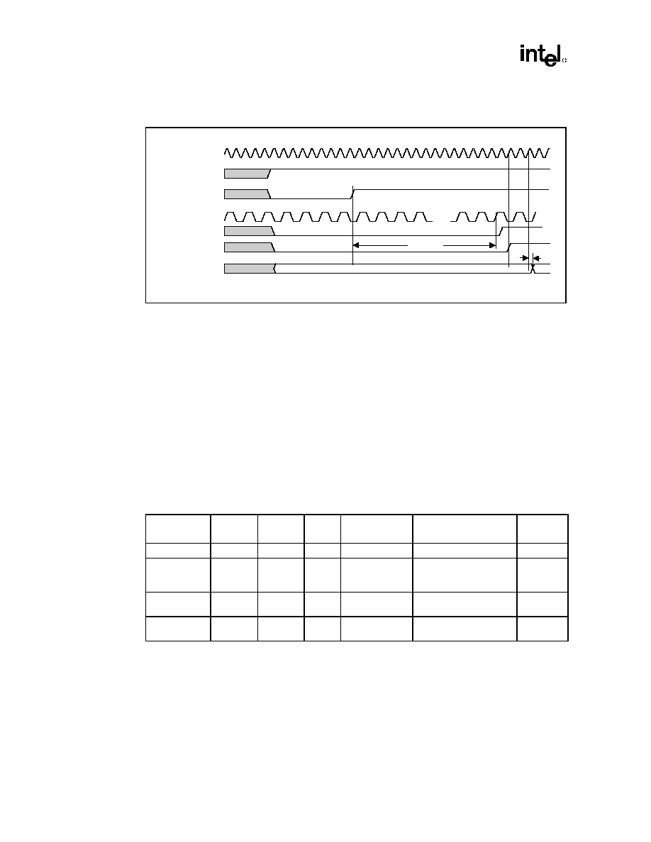
Functional Description
4-28
82443GX Host Bridge Datasheet
4.8.2.3
82443GX Straps
The 82443GX strapping options are latched in the rising edge of PCIRST#.
4.8.3
Suspend Resume
4.8.3.1
Suspend Resume protocols
The suspend resume sequences are indicated to the 82443GX by the PIIX4E, using SUS_STAT#,
and PCIRST#. In addition, the 82443GX contains NREF_EN and CRst_En configuration bits that
participate in the suspend resume sequences. As a result of suspend resume, the 82443GX
performs the following activities: Changing its refresh mode, performing internal and CPU reset
and Isolate or re-enable normal IO buffers.
Figure 4-5. External Glue Logic Drives CPU Clock Ratio Straps
1 2
1 m s
1
3 3 , 3 3 3
....
2
H C L K
S U S _ D I S s t r a p
CPU strap values from external Glue Logic
Suspend disable value latched when PCIRST#
P C I R S T #
P C L K
C R E S E T #
C P U s t r a p s
p_creset#
0
0
gx_time2.vsd
Table 4-15. Suspend / Resume Events and Activities
State
SUSTAT#
PCIRST#
CrstEn
RESET
REFRESH
IO
BUFFERS
ON
assert
inactive
-
-
switch to suspend refresh
isolate
POSCL/STR
deassert
active
-
reset exclude
resume/ref logic
suspend refresh
NREF_EN remains
inactive
enable
POS
deassert
inactive
0
no resets
auto switch to normal ref
NREF_EN is set
enable
POSCCL
deassert
inactive
1
reset CPU only
auto switch to normal ref
NREF_EN is set
enable

82443GX Host Bridge Datasheet
4-29
Functional Description
4.8.3.2
Suspend Refresh
SDRAM Suspend Refresh
When the 82443GX is configured for 4 DIMMs, a single GCKE (global CKE) is provided to allow
an external device to correctly drive the external CKE signals to the SDRAM devices. A detailed
description of the DRAM signal functions is given in the Chapter 2, "Signal Description".
For the Registered DIMMs the CKE function is not supported. The stacking technology used for
registered DIMMs prohibits the use of the CKE function. For registered DIMMs, components are
stacked on top of one another. The stacked components are physically in the same row, but
logically in separate rows. The stacked components connect all pins together, except for the CS#
pin, in order to address components in different rows. Since the CKE pins for the components are
connected together, and the components are logically in different rows, the CKE function is not
supported.
4.8.4
Clock Control Functions
The 82443GX implements an independent Clock Gating power savings feature to reduce its own
average power consumption. The 82443GX clock gating functions works along with the primary
PCI bus CLKRUN# function.
The Clock Gating function is enabled by setting the GCLKEN Configuration bit. This function
default value is 0. The AGP interface's clock domain can be permanently disabled by the AGP_DIS
configuration bit. This allows further power savings in systems that AGP is not used.
CLKRUN Clocking States
There are three states in the CLKRUN# protocol:
∑
Clock Running: The clock is running and the bus is operational.
∑
Clock Stop Request: The central resource has indicated on the CLKRUN# line that the clock
is about to stop.
∑
Clock Stopped: The clock is stopped with CLKRUN# being monitored for a restart.

Functional Description
4-30
82443GX Host Bridge Datasheet
4.8.5
SMRAM
SMRAM ranges
The 82443GX supports the use of main memory as System Management RAM (SMRAM)
enabling the use of System Management Mode. There are two SMRAM options: Compatible
SMRAM (C_SMRAM) and Extended SMRAM (E_SMRAM). System Management RAM
(SMRAM) space provides a memory area that is available for the SMI handler's and code and data
storage. This memory resource is normally hidden from the operating system so that the processor
has immediate access to this memory space upon entry to SMM. 82443GX provides three
SMRAM options:
∑
Below 1 MB option that supports compatible SMI handlers.
∑
Above 1 MB option that allows new SMI handlers to execute with write-back cacheable
SMRAM.
∑
Optional larger write-back cacheable T_SEG area from 128KB to 1MB in size above 1 MB
that is reserved from the highest area in system DRAM memory. The above 1 MB solutions
require changes to compatible SMRAM handlers code to properly execute above 1 MB.
Compatible SMRAM (C_SMRAM)
This is the traditional SMRAM feature supported in Intel AGPsets. When this function is enabled
via C_BASE_SEG[2:0]=010 and G_SMRAME=1 of the SMRAMC register, the 82443GX
reserves 000A0000h through 000BFFFFh (A and B segments) of the main memory for use as non-
cacheable SMRAM.
The SMI handler can set the CLS bit to enable data accesses to aliased memory space, while code
fetches access the SMRAM space.
Extended SMRAM (E_SMRAM)
This feature in the 82443GX extend the SMRAM space up to 1 MB and provide write-back
cacheability.
The TSEG size is 128 KBs, 256 KBs, 512 KBs or 1 MB, as defined by TSEG_SZ[1:0] of the
SMRAMC register.
The CPU can access these memory ranges by one of the following mechanisms:
∑
The processor can access SMRAM while in the SMM mode. A processor access to while not
in SMM and with while the D_OPN bit is reset will be forwarded to PCI bus and a status bit is
set in the SMRAMC register.
∑
The processor can access SMRAM while the D_OPN bit is set.

82443GX Host Bridge Datasheet
5-1
Pinout and Package Information
P i n o u t a n d Pa ck ag e I n fo r m a t i o n
5
5.1
82443GX Pinout
Figure 5-1 and Figure 5-2 show the ball footprint of the 82443GX package. These figures represent
the pinout by ball number. For an alphabetical list of the pinout by signal name refer to Table 5-1.

Pinout and Package Information
5-2
82443GX Host Bridge Datasheet
Figure 5-1. 82443GX Pinout (Top View≠left side)
1
2
3
4
5
6
7
8
9
10
11
12
13
A
VSS
AD20
PCIRST#
AD25
AD29
PREQ0#
HD56#
HD62#
HD55#
HD54#
HD49#
HD47#
HD40#
B
VCC
PCLKIN
AD22
AD27
AD28
PHOLD#
HD50#
HD61#
HD63#
HD53#
HD48#
HD42#
HD36#
C
AD19
REFVCC
AD21
C/BE3#
VSS
AD31
PREQ1#
HD52#
VSS
HD60#
HD59#
HD51#
HD44#
D
AD16
AD18
AD17
AD23
AD26
PHLDA#
PGNT1#
PREQ3#
HD58#
PREQ4#
HD46#
HD41#
HD39#
E
IRDY#
FRAME#
VSS
C/BE2#
AD24
AD30
PGNT0#
PGNT3#
PGNT4#
PGNT2#
HD57#
VSS
HD45#
F
SERR#
PLOCK#
DEVSEL#
STOP#
TRDY#
VSS
VCC
VSS
VCC
PREQ2#
G
AD13
AD14
C/BE1#
AD15
PAR
VCC
H
AD8
AD7
AD10
AD12
AD11
VSS
J
AD5
AD6
VSS
C/BE0#
AD9
VCC
K
SBA0
AD1
AD3
AD2
AD4
AD0
L
ST2
ST1
GGNT#
ST0
GREQ#
VCC
VSS
VCC
M
SBA2
SBA1
PIPE#
RBF#
VSS
VSS
VCC
VSS
N
VSS
SBA3
SBSTB
AGPREF
GCLKIN
VCC
VSS
VSS
P
VCC
SBA4
SBA6
SBA5
GCLKO
VCC
VSS
VSS
R
SBA7
GAD31
GAD29
GAD30
VSS
VSS
VCC
VSS
T
GAD27
GAD26
GAD24
GAD25
ADSTB_B
VCC
VSS
VCC
U
GAD23
GC/BE3#
GAD22
GAD21
GAD19
GAD28
V
GAD20
GAD17
VSS
GC/BE2#
GIRDY#
VCC
W
GAD16
GAD18
GFRAME#
GTRDY#
GDEVSEL#
VSS
Y
GSTOP#
GPAR
GAD15
GC/BE1#
GAD14
VCC
AA
GAD13
GAD12
GAD10
GAD11
GAD9
VSS
VCC
VSS
VCC
MECC1
AB
GAD8
GC/BE0#
VSS
GAD7
GAD0
MD34
MD5
MD8
MD9
MD12
MD46
VSS
SCASB#
AC
GAD6
ADSTB_A
GAD5
CLKRUN#
MD32
MD35
MD6
MD39
MD10
MD13
MD47
WEB#
DQMA1
AD
GAD4
GAD3
GAD2
SUSTAT#
VSS
MD3
MD37
MD40
VSS
MD44
MD15
MECC5
DQMA0
AE
VCC
GAD1
WSC#
MD1
MD33
MD4
MD38
MD42
MD11
MD45
MECC0
WEA#
DQMB1
AF
VSS
VCC
GXPWROK
MD0
MD2
MD36
MD7
MD41
MD43
MD14
MECC4
SCASA#
VSS

82443GX Host Bridge Datasheet
5-3
Pinout and Package Information
Figure 5-2. 82443GX Pinout (Top View≠right side)
14
15
16
17
18
19
20
21
22
23
24
25
26
VSS
HD33#
HD31#
HD27#
HD19#
HD20#
HD10#
HD6#
HD3#
HA29#
HA24#
HA22#
VSS
A
HD43#
HD32#
HD29#
HD25#
HD21#
HD18#
HD12#
HD8#
HD0#
CPURST#
HA27#
HA20#
BREQ0#
B
HD37#
HD28#
HD26#
HD22#
VSS
HD17#
HD7#
HD5#
VSS
HA26#
HA28#
HA23#
HA21#
C
HD34#
HD35#
HD30#
HD24#
HD16#
HD15#
HD14#
HD4#
HD1#
HA31#
HA25#
HA18#
HA19#
D
HD38#
VSS
GTLREFB
HD23#
HD13#
HD11#
HD9#
HD2#
HA30#
HA15#
VSS
HA17#
HA16#
E
VTTB
VCC
VSS
VCC
VSS
HA11#
HA12#
HA13#
HA14#
HA8#
F
VCC
HA10#
HA5#
HA7#
HA3#
HA9#
G
VSS
HA4#
HA6#
BNR#
HTRDY#
BPRI#
H
VCC
HREQ0#
HREQ1#
VSS
HREQ4#
DEFER#
J
ADS#
HLOCK#
DRDY#
HREQ2#
HREQ3#
RS0#
K
VCC
VSS
VCC
HITM#
DBSY#
HIT#
RS2#
RS1#
L
VSS
VCC
VSS
VSS
GTLREFA
VTTA
TESTIN#
CRESET#
M
VSS
VSS
VCC
VCC
HCLKIN
VSS
MD31
VCC
N
VSS
VSS
VCC
NC
MD30
MD62
MD63
VSS
P
VSS
VCC
VSS
VSS
MD60
MD28
MD29
MD61
R
VCC
VSS
VCC
MD25
MD26
MD57
MD58
MD27
T
MD59
MD54
MD24
MD23
MD55
MD56
U
VCC
MD51
MD52
VSS
MD53
MD22
V
VSS
MD50
MD18
MD19
MD21
MD20
W
VCC
MECC7
MD48
MD16
MD17
MD49
Y
SRASB#
VCC
VSS
VCC
VSS
DQMA6
MECC2
DQMA7
MECC6
MECC3
AA
CSA0#
VSS
MAA1
MAB3#
MAB6#
MAB7#
MAB10
DCLKO
NC
CSB5#
VSS
VSS
DQMA3
AB
DQMA5
CSA3#
MAB1#
MAA3
MAA7
MAA8
MAB9#
MAA12
FENA
CKE4
CSB3#
DQMA2#
CSB4#
AC
DQMB5
CSA4#
MAB0#
MAB2#
VSS
MAB5#
MAA10
MAB12#
VSS
CKE3
CSB1#
DCLKWR
CSB2#
AD
DQMA4
CSA2#
CSA5#
MAA2
MAB4#
MAA5
MAA9
MAB11#
MAA14
MAB14
CKE2
CSB0#
VCC
AE
VCC
CSA1#
SRASA#
MAA0
MAA4
MAA6
MAB8#
MAA11
MAB13
GCKE
CKE5
MAA13
VSS
AF
Pinout and Package Information
5-4
82443GX Host Bridge Datasheet
Table 5-1. 82443GX Alphabetical BGA Pin List (Sheet 1 of 4)
Signal Name
Pin
Signal Name
Pin
Signal Name
Pin
AD0
K6
C/BE2#
E4
GAD1
AE2
AD1
K2
C/BE3#
C4
GAD2
AD3
AD2
K4
FENA
AC22
GAD3
AD2
AD3
K3
GCKE
AF23
GAD4
AD1
AD4
K5
CSA6
AE24
GAD5
AC3
AD5
J1
CSA7
AD23
GAD6
AC1
AD6
J2
CSB6
AC23
GAD7
AB4
AD7
H2
CSB7
AF24
GAD8
AB1
AD8
H1
CLKRUN#
AC4
GAD9
AA5
AD9
J5
CPURST#
B23
GAD10
AA3
AD10
H3
CRESET#
M26
GAD11
AA4
AD11
H5
CSA0#
AB14
GAD12
AA2
AD12
H4
CSA1#
AF15
GAD13
AA1
AD13
G1
CSA2#
AE15
GAD14
Y5
AD14
G2
CSA3#
AC15
GAD15
Y3
AD15
G4
CSA4#
AD15
GAD16
W1
AD16
D1
CSA5#
AE16
GAD17
V2
AD17
D3
CSB0#
AE25
GAD18
W2
AD18
D2
CSB1#
AD24
GAD19
U5
AD19
C1
CSB2#
AD26
GAD20
V1
AD20
A2
CSB3#
AC24
GAD21
U4
AD21
C3
CSB4#
AC26
GAD22
U3
AD22
B3
CSB5#
AB23
GAD23
U1
AD23
D4
DBSY#
L23
GAD24
T3
AD24
E5
DCLKO
AB21
GAD25
T4
AD25
A4
DCLKWR
AD25
GAD26
T2
AD26
D5
DEFER#
J26
GAD27
T1
AD27
B4
DEVSEL#
F3
GAD28
U6
AD28
B5
DQMA0
AD13
GAD29
R3
AD29
A5
DQMA1
AC13
GAD30
R4
AD30
E6
DQMA2
AC25
GAD31
R2
AD31
C6
DQMA3
AB26
GC/BE0#
AB2
ADS#
K21
DQMA4
AE14
GC/BE1#
Y4
ADSTB_A
AC2
DQMA5
AC14
GC/BE2#
V4
ADSTB_B
T5
DQMA6
AA22
GC/BE3#
U2
AGPREF
N4
DQMA7
AA24
GCLKIN
N5
BNR#
H24
DQMB1
AE13
GCLKO
P5
BPRI#
H26
DQMB5
AD14
GDEVSEL#
W5
BREQ0#
B26
DRDY#
K23
GFRAME#
W3
C/BE0#
J4
FRAME#
E2
GGNT#
L3
C/BE1#
G3
GAD0
AB5
GIRDY#
V5

82443GX Host Bridge Datasheet
5-5
Pinout and Package Information
GPAR
Y2
HD5#
C21
HD46#
D11
GREQ#
L5
HD6#
A21
HD47#
A12
GSTOP#
Y1
HD7#
C20
HD48#
B11
GTLREFA
M23
HD8#
B21
HD49#
A11
GTLREFB
E16
HD9#
E20
HD50#
B7
GTRDY#
W4
HD10#
A20
HD51#
C12
HA3#
G25
HD11#
E19
HD52#
C8
HA4#
H22
HD12#
B20
HD53#
B10
HA5#
G23
HD13#
E18
HD54#
A10
HA6#
H23
HD14#
D20
HD55#
A9
HA7#
G24
HD15#
D19
HD56#
A7
HA8#
F26
HD16#
D18
HD57#
E11
HA9#
G26
HD17#
C19
HD58#
D9
HA10#
G22
HD18#
B19
HD59#
C11
HA11#
F22
HD19#
A18
HD60#
C10
HA12#
F23
HD20#
A19
HD61#
B8
HA13#
F24
HD21#
B18
HD62#
A8
HA14#
F25
HD22#
C17
HD63#
B9
HA15#
E23
HD23#
E17
HIT#
L24
HA16#
E26
HD24#
D17
HITM#
L22
HA17#
E25
HD25#
B17
HLOCK#
K22
HA18#
D25
HD26#
C16
HREQ0#
J22
HA19#
D26
HD27#
A17
HREQ1#
J23
HA20#
B25
HD28#
C15
HREQ2#
K24
HA21#
C26
HD29#
B16
HREQ3#
K25
HA22#
A25
HD30#
D16
HREQ4#
J25
HA23#
C25
HD31#
A16
HTRDY#
H25
HA24#
A24
HD32#
B15
IRDY#
E1
HA25#
D24
HD33#
A15
MAA0
AF17
HA26#
C23
HD34#
D14
MAA1
AB16
HA27#
B24
HD35#
D15
MAA2
AE17
HA28#
C24
HD36#
B13
MAA3
AC17
HA29#
A23
HD37#
C14
MAA4
AF18
HA30#
E22
HD38#
E14
MAA5
AE19
HA31#
D23
HD39#
D13
MAA6
AF19
HCLKIN
N23
HD40#
A13
MAA7
AC18
HD0#
B22
HD41#
D12
MAA8
AC19
HD1#
D22
HD42#
B12
MAA9
AE20
HD2#
E21
HD43#
B14
MAA10
AD20
HD3#
A22
HD44#
C13
MAA11
AF21
HD4#
D21
HD45#
E13
MAA12
AC21
Table 5-1. 82443GX Alphabetical BGA Pin List (Sheet 2 of 4)
Signal Name
Pin
Signal Name
Pin
Signal Name
Pin

Pinout and Package Information
5-6
82443GX Host Bridge Datasheet
MAA13
AF25
MD24
U23
MECC1
AA10
MAA14
AE22
MD25
T22
MECC2
AA23
MAB0#
AD16
MD26
T23
MECC3
AA26
MAB1#
AC16
MD27
T26
MECC4
AF11
MAB2#
AD17
MD28
R24
MECC5
AD12
MAB3#
AB17
MD29
R25
MECC6
AA25
MAB4#
AE18
MD30
P23
MECC7
Y22
MAB5#
AD19
MD31
N25
NC
AB22
MAB6#
AB18
MD32
AC5
NC
P22
MAB7#
AB19
MD33
AE5
PAR
G5
MAB8#
AF20
MD34
AB6
PCIRST#
A3
MAB9#
AC20
MD35
AC6
PCLKIN
B2
MAB10
AB20
MD36
AF6
PGNT0#
E7
MAB11#
AE21
MD37
AD7
PGNT1#
D7
MAB12#
AD21
MD38
AE7
PGNT2#
E10
MAB13
AF22
MD39
AC8
PGNT3#
E8
MAB14
AE22
MD40
AD8
PGNT4#
E9
MD0
AF4
MD41
AF8
PHLDA#
D6
MD1
AE4
MD42
AE8
PHOLD#
B6
MD2
AF5
MD43
AF9
PIPE#
M3
MD3
AD6
MD44
AD10
PLOCK#
F2
MD4
AE6
MD45
AE10
PREQ0#
A6
MD5
AB7
MD46
AB11
PREQ1#
C7
MD6
AC7
MD47
AC11
PREQ2#
F10
MD7
AF7
MD48
Y23
REQ3#
D8
MD8
AB8
MD49
Y26
PREQ4#
D10
MD9
AB9
MD50
W22
RBF#
M4
MD10
AC9
MD51
V22
REFVCC
C2
MD11
AE9
MD52
V23
RS0#
K26
MD12
AB10
MD53
V25
RS1#
L26
MD13
AC10
MD54
U22
RS2#
L25
MD14
AF10
MD55
U25
SBSTB
N3
MD15
AD11
MD56
U26
SBA0
K1
MD16
Y24
MD57
T24
SBA1
M2
MD17
Y25
MD58
T25
SBA2
M1
MD18
W23
MD59
U21
SBA3
N2
MD19
W24
MD60
R23
SBA4
P2
MD20
W26
MD61
R26
SBA5
P4
MD21
W25
MD62
P24
SBA6
P3
MD22
V26
MD63
P25
SBA7
R1
MD23
U24
MECC0
AE11
SCASA#
AF12
Table 5-1. 82443GX Alphabetical BGA Pin List (Sheet 3 of 4)
Signal Name
Pin
Signal Name
Pin
Signal Name
Pin
82443GX Host Bridge Datasheet
5-7
Pinout and Package Information
SCASB#
AB13
VCC
V21
VSS
N14
SERR#
F1
VCC
Y6
VSS
N15
SRASA#
AF16
VCC
Y21
VSS
N24
SRASB#
AA17
VCC
AA7
VSS
P12
ST0
L4
VCC
AA9
VSS
P13
ST1
L2
VCC
AA18
VSS
P14
ST2
L1
VCC AA20
VSS
P15
STOP#
F4
VCC
AE1
VSS
P26
GXPWROK
AF3
VCC
AE26
VSS
R5
SUSTAT#
AD4
VCC
AF2
VSS
R11
TESTIN#
M25
VCC
AF14
VSS
R13
TRDY#
F5
VSS
A1
VSS
R14
VCC
B1
VSS
A14
VSS
R16
VCC
F7
VSS
A26
VSS
R22
VCC
F9
VSS
C5
VSS
T12
VCC
F18
VSS
C9
VSS
T15
VCC
F20
VSS
C18
VSS
V3
VCC
G6
VSS
C22
VSS
V24
VCC
G21
VSS
E3
VSS
W6
VCC
J6
VSS
E12
VSS
W21
VCC
J21
VSS
E15
VSS
AA6
VCC
L11
VSS
E24
VSS
AA8
VCC
L13
VSS
F6
VSS
AA19
VCC
L14
VSS
F8
VSS
AA21
VCC
L16
VSS
F19
VSS
AB3
VCC
M12
VSS
F21
VSS
AB12
VCC
M15
VSS
H6
VSS
AB15
VCC
N11
VSS
H21
VSS
AB24
VCC
N16
VSS
J3
VSS
AB25
VCC
N22
VSS
J24
VSS
AD5
VCC
N26
VSS
L12
VSS
AD9
VCC
P1
VSS
L15
VSS
AD18
VCC
P11
VSS
M5
VSS
AD22
VCC
P16
VSS
M11
VSS
AF1
VCC
R12
VSS
M13
VSS
AF13
VCC
R15
VSS
M14
VSS
AF26
VCC
T11
VSS
M16
VTTA
M24
VCC
T13
VSS
M22
VTTB
F17
VCC
T14
VSS
N1
WEA#
AE12
VCC
T16
VSS
N12
WEB#
AC12
VCC
V6
VSS
N13
WSC#
AE3
Table 5-1. 82443GX Alphabetical BGA Pin List (Sheet 4 of 4)
Signal Name
Pin
Signal Name
Pin
Signal Name
Pin
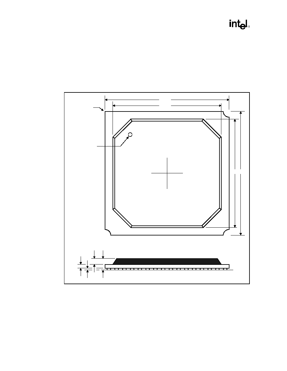
Pinout and Package Information
5-8
82443GX Host Bridge Datasheet
5.2
Package Dimensions
This specification outlines the mechanical dimensions for the 82443GX Host Bridge. The package
is a 492 ball grid array (BGA).
Figure 5-3. 82443GX BGA Package Dimensions--Top and Side Views
Pin A1 I.D.
P i n A 1 c o r n e r
D
D 1
E
E 1
T o p V i e w
A
A 2
A 1
c
S i d e V i e w
4 9 2 _ p k g 1 . v s d
82443GX Host Bridge Datasheet
5-9
Pinout and Package Information
Figure 5-4. 82443GX BGA Package Dimensions--Bottom Views
Table 5-2. 82443GX Package Dimensions (492 BGA)
Symbol
e=1.27 mm (solder ball pitch)
Note
Min
Nominal
Max
A
2.17
2.38
2.59
A1
0.50
0.60
0.70
A2
1.12
1.17
1.22
D
34.80
35.00
35.20
D1
29.75
30.00
30.25
E
34.80
35.00
35.20
E1
29.75
30.00
30.25
I
1.63 REF.
J
1.63 REF.
M
26 x 26 Matrix
N
4.92
b
0.60
0.75
0.90
c
0.55
0.61
0.67
A
B
C
D
E
F
G
H
J
K
L
P
R
T
U
V
Y
AB
AA
AC
2
10
16
20
22
3
5
7
9
11
13
15
17
19
1
21
23
AD
AE
N
25
24
W
4
6
18
8
12
14
M
AF
26
Pin A1 corner
b
e
j
l
468 BGA
Bottom View

Pinout and Package Information
5-10
82443GX Host Bridge Datasheet
82443GX Host Bridge Datasheet
6-1
Testability
Testability
6
This section provides information about the testability features of the 82443GX.
6.1
Test Mode Activation
The primary test mode is enabled via the TESTIN# pin. To enable a test mode, the TESTIN# input
pin is asserted low and a 5-bit binary pattern is presented on the PCI PREQ[4:0]# input pins. The
following tables show the PREQ[4:0]# signal encoding for test modes enabled via TESTIN# pin.
Normal Operation is the normal operating mode of 82443GX. The 82443GX enters this mode
during power up (as long as the TESTIN# pin is tied off to high) and stays in this mode for the
duration of its operation.
No primary test mode is accessible during normal operation. The Tristate All Outputs test mode is
used to tristate all bi-directional and output-only pins. This can be used as a debugging technique
on the motherboard. During this test mode, all pullups and pulldowns are also disabled.
Figure 6-1 shows the sequence required to enable a primary test mode. Note that the TESTIN#
input pin acts as a latch enable, and the PREQ[4:0]# pins act as latch inputs. The test mode is
decoded from the output of the latch.
Table 6-1. Test Modes
PREQ[2:0]#
Test Mode Enabled
000
NAND Chain A
001
NAND Chain B
110
Normal Operation
111
Normal Operation
Table 6-2. Output Modes
PREQ[4:3]#
Test Mode Enabled
00
Tristate all Outputs
11
Enable all Outputs (default)
Testability
6-2
82443GX Host Bridge Datasheet
6.2
Tester Powerup Sequence
Figure 6-2 shows the typical powerup sequence of 443GX on a tester. At time 0, PCIRST# and
TESTIN# must be asserted. The GXPWROK signal must also be asserted to indicate that a cold
reset is in progress. Once PCIRST# is deasserted TESTIN# can also be safely deasserted on the
fourth DCLKWR positive edge. PCIRST# and TESTIN# should not deassert at the same time
because a race condition prevents the circuit from guaranteeing proper latching of primary test
modes.
Figure 6-1. Waveform of Test Mode
test_tm1.vsd
T e s t m o d e a c t i v a t i o n w i t h o u t c o l d r e s e t ( t o g g l i n g o f G X P W R O K)
NAND Chain A
D C L K W R
G X P W R O K
P C I R S T #
T E S T I N #
P R E Q [ 4 : 0 ] #
T e s t M o d e
NAND Chain A
Figure 6-2. Typical power-up sequence
test_tm2.vsd
D C L K W R
1
2
3
4
5
6
7
8
9
1 0
1 1
1 2
1 3
1 4
G X P W R O K
P C I R S T #
T E S T I N #
P R E Q [ 2 : 0 ] #
P R E Q [ 4 : 3 ] #
S U S T A T #
T e s t M o d e
m i n o f 4 D C L K W R p e r i o d s
m i n o f 8 D C L K W R p e r i o d s
m i n o f 4 D C L K W R p e r i o d s
Output Enable
N o r m a l O p e r a t i o n
O u t p u t E n a b l e
Async Tristate
s u s p e n d m o d e d i s a b l e d a s l o n g a s S U S T A T # r e m a i n s d e a s s e r t e d
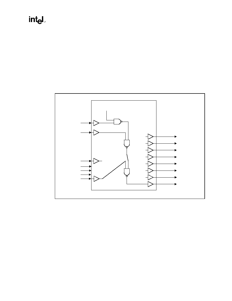
82443GX Host Bridge Datasheet
6-3
Testability
6.3
Test Mode Details
6.3.1
Nand CHAIN A
The NAND chain A test mode is used for board level connectivity test. Its main purpose is to
detect connectivity shorts between adjacent pins and to check proper bonding between I/O pads
and I/O pins. Figure 6-3 is a conceptual diagram of the NAND chain.
To help reduce the board level test cost, the NAND chain is limited to 60 pins per chain. This is
accomplished by implementing 9 separate NAND chains.
Figure 6-4 shows an example NAND tree test. At first, all the input pins are driven to logic 1. Next,
each input pin is driven to logic 0, in a sequence, so that the output pin, in this case SBA[0],
toggles. By observing the NAND chain output pin, one can detect shorted and unconnected pins.
Figure 6-3. NAND Chain A0 Connectivity
test_cha.vsd
H A 2 1 #
H A 6 #
H A 4 #
S B A [ 0 ]
V c c
8 2 4 4 3 G X
O u t p u t s
Inputs
S B A [ 1 ]
S B A [ 2 ]
S B A [ 3 ]
S B A [ 4 ]
S B A [ 5 ]
S B A [ 6 ]
S B A [ 7 ]
N A N D C h a i n A 0
A D 2 1
Testability
6-4
82443GX Host Bridge Datasheet
Figure 6-4. Waveform of NAND Chain A7 Test
An example of NAND chain A7 bein g exercised
G G N T #
S T 2
G C L K I N
G A D 2 6
G C L K O
G A D 2 4
G C B E 3 #
G A D 3 0
G A D 2 2
G A D 2 0
G A D S T B #
G A D 1 8
G S T O P #
G I R D Y #
G A D 2 8
G C B E 1 #
G A D 1 2
G A D 1 0
G A D 8
G A D 1 4
G A D 6
G A D 1
G A D 4
G A D 3
G A D 2
NAND chain out SBA[7]
test_tm3.vsd

82443GX Host Bridge Datasheet
6-5
Testability
Signals not included in NAND chain A or B are listed in Table 6-3. The pin assignments for NAND
chain A are shown in Table 6-4 and Table 6-5.
Note:
Chains A4 & A5 must always go through chains A8 and A9 respectively before they comes out of
SBA[4] and SBA[5].
Table 6-3. Signals Not Included in NAND chain A or B
Signals
Purpose
GXPWROK
Used for cold reset
PCIRST#
Used for cold and warm reset
TESTIN#
Used to enter NAND chain A and B test modes
Table 6-4. Nandtree A Outputs
Signals
Purpose
SBA[0]
NAND Chain A0 Output
SBA[1]
NAND Chain A1 Output
SBA[2]
NAND Chain A2 Output
SBA[3]
NAND Chain A3 Output
SBA[4]
NAND Chain A4 and A8 Output
SBA[5]
NAND Chain A5 and A9 Output
SBA[6]
NAND Chain A6 Output
SBA[7]
NAND Chain A7 Output
Table 6-5. NAND Chains A
#
Chain
#A0
Chain
#A1
Chain
#A2
Chain
#A3
Chain
#A4
Chain
#A5
Chain
#A6
Chain
#A7
Chain
#A8
Chain
#A9
1
HA21#
HA15#
PGNT3#
AD30
DQMB1
MAA0
RBF#
GGNT#
MAB14
DQMA2
2
HA6#
HREQ0#
PGNT0#
AD24
DQMB5
MAA2
GREQ#
ST2
MECC2
DQMA3
3
HA4#
HA18#
AD19
TRDY#
CSA7#
MAA4
ST1
GCLKIN
DQMA6
MECC6
4
HA28#
HA23#
AD17
AD18
CSA6#
MAA6
PIPE#
GAD26
DQMA7
MECC7
5
HA20#
HA31#
AD11
AD16
CSB6#
MAA5
ST0
GCLKO
MD48
MECC3
6
HA26#
BREQ0#
PAR
FRAME#
CSB1#
MAA8
SB-STB
GAD24
MD50
MD16
7
HA27#
HA10#
C/BE2#
IRDY#
CSB0#
MAA9
GAD31
GC/BE3#
MD49
MD17
8
HA30#
HA22#
AD15
AD12
CSB2#
MAA1
GAD29
GAD30
MD51
MD18
9
HA24#
HD1#
STOP#
PLOCK#
CSB3#
MAA10
GAD27
GAD22
MD52
MD19
10
CPURST#
HA11#
DEVSEL#
C/BE1#
CSB5#
MAA3
GAD23
GAD20
MD53
MD21
11
HD32#
HD2#
SERR#
AD14
DCLKO
MAA11
GAD25
GAD-STBB
MD59
MD20
12
HD33#
HA29#
AD13
AD10
CSB4#
MAA12
GAD17
GAD16
MD55
MD22
13
HD37#
HD4#
AD9
AD8
GCKE
GC/BE2#
GAD18
MD54
MD23
14
HD43#
HD0#
AD0
AD4
CSB7#
GFRAME#
GSTOP#
MD57
MD24
15
HD40#
HD3#
AD7
AD6
MAA7
GTRDY#
GIRDY#
MD58
MD27
16
HD36#
HD8#
C/BE0#
AD2
MAA13
GAD21
GAD28
MD56
MD28
17
HD35#
HD5#
AD5
AD1
MAA14
GPAR
GC/BE1#
MD61
MD29
18
HD44#
HD9#
AD3
CLKRUN#
GAD19
GAD12
MD62
MD25
19
HD34#
HD6#
MD34
WSC#
GAD15
GAD10
MD63
MD31

Testability
6-6
82443GX Host Bridge Datasheet
20
HD47#
HD7#
MD32
SUSTAT#
GAD13
GAD8
CRESET#
MD26
21
HD42#
HD10#
MD35
MD1
GDEVSEL#
GAD14
MD60
RS1#
22
HD38#
HD12#
MD33
MD0
GAD11
GAD6
RS0#
MD30
23
HD51#
HD14#
MD36
MD5
GAD7
GAD1
RS2#
HCLKIN
24
HD49#
HD15#
MD37
MD2
GC/BE0#
GAD4
HREQ3#
HIT#
25
HD54#
HD17#
MD38
MD3
GAD-STBA
GAD3
HREQ2#
DBSY#
26
HD48#
HD11#
MD42
MD4
GAD5
GAD2
HREQ4#
DEFER#
27
HD45#
HD18#
MD40
MD6
GAD9
HREQ1#
HITM#
28
HD59#
HD13#
MD39
MD8
GAD0
BPRI#
DRDY#
29
HD39#
HD20#
MD41
MD7
BNR#
HTRDY#
30
HD53#
HD16#
MD44
MD9
HLOCK#
HA9#
31
HD60#
HD21#
MD43
MD11
HA5#
HA3#
32
HD55#
HD19#
MD45
MD15
HA14#
HA7#
33
HD63#
HD22#
WEB#
MD10
HA13#
HA8#
34
HD41#
HD25#
SCASA#
MECC0
ADS#
HA12#
35
HD58#
HD23#
DQMA4
MD14
HA16#
HA17#
36
HD62#
HD26#
MD46
MECC1
HA19#
37
HD46#
HD29#
MD47
MECC4
HA25#
38
HD61#
HD27#
SCASB#
MD12
39
HD57#
HD31#
MAB0#
MECC5
40
HD52#
HD28#
MAB2#
WEA#
41
HD56#
HD24#
MAB4#
MD13
42
HD50#
HD30#
MAB1#
DQMA0
43
PREQ1#
PGNT1#
MAB5#
CSA1#
44
PREQ0#
PREQ4#
MAB8#
CSA2#
45
PGNT2#
PHLDA#
MAB9#
CSA4#
46
PHOLD#
PREQ2#
MAB11#
CSA3#
47
AD31
AD28
MAB12#
SRASA#
48
AD29
AD26
MAB3#
DQMA1
49
AD25
C/BE3#
MAB13
CSA5#
50
PGNT4#
AD22
MAB6#
CSA0#
51
AD27
REQ3#
MAB7#
DQMA5
52
AD23
AD20
MAB10
FENA
53
AD21
PCLKIN
DCLKWR
SRASB#
Table 6-5. NAND Chains A
#
Chain
#A0
Chain
#A1
Chain
#A2
Chain
#A3
Chain
#A4
Chain
#A5
Chain
#A6
Chain
#A7
Chain
#A8
Chain
#A9
82443GX Host Bridge Datasheet
6-7
Testability
6.3.2
Nand CHAIN B
The NAND chain B test mode is used to test the SBA[7:0] pins. These pins are outputs during the
NAND chain A test mode and are not tested in that mode. In NAND chain B test mode, the
SBA[7:0] signals become inputs and the CRESET# pin becomes the output.
Table 6-6. NAND Chain B Output
Signals
Purpose
CRESET#
NAND CHAIN B0 Output
Table 6-7. NAND Chain B
#
Chain #B0
1
SBA0
2
SBA1
3
SBA2
4
SBA3
5
SBA4
6
SBA6
7
SBA5
8
SBA7
Figure 6-5. NAND Chain B Test Mode
test_chb.vsd
SBA[0]
SBA[1]
SBA[7]
C R E S E T #
V c c
82443GX
Outputs
Inputs
NAND Chain B0

United States and Canada
Intel Corporation
Robert Noyce Building
2200 Mission College Boulevard
P.O. Box 58119
Santa Clara, CA 95052-8119
USA
Phone: (800) 628-8686
Europe
Intel Corporation (U.K.) Ltd.
Pipers Way
Swindon
Wiltshire SN3 1RJ
UK
Phone:
England
(44) 1793 403 000
Germany
(49) 89 99143 0
France
(33) 1 4571 7171
Italy
(39) 2 575 441
Israel
(972) 2 589 7111
Netherlands
(31) 10 286 6111
Sweden
(46) 8 705 5600
Asia Pacific
Intel Semiconductor Ltd.
32/F Two Pacific Place
88 Queensway, Central
Hong Kong, SAR
Phone: (852) 2844 4555
Japan
Intel Kabushiki Kaisha
P.O. Box 115 Tsukuba-gakuen
5-6 Tokodai, Tsukuba-shi
Ibaraki-ken 305
Japan
Phone: (81) 298 47 8522
South America
Intel Semicondutores do Brazil
Rua Florida 1703-2 and CJ22
CEP 04565-001 Sao Paulo-SP
Brazil
Phone: (55) 11 5505 2296
For More Information
To learn more about Intel Corporation, visit our site
on the World Wide Web at www.intel.com
Intel around the world