 | –≠–ª–µ–∫—Ç—Ä–æ–Ω–Ω—ã–π –∫–æ–º–ø–æ–Ω–µ–Ω—Ç: 440ZX | –°–∫–∞—á–∞—Ç—å:  PDF PDF  ZIP ZIP |
Document Outline
- Intel Æ 440ZX AGPset:
- Intel 82443ZX Features
- Intel 82443ZX Simplified Block Diagram
- Contents
- Architectural Overview
- Signal Description
- 2.1 Host Interface Signals
- 2.2 DRAM Interface
- 2.3 PCI Interface (Primary)
- 2.4 Primary PCI Sideband Interface
- 2.5 AGP Interface Signals
- 2.6 Clocks, Reset, and Miscellaneous
- 2.7 Power-Up/Reset Strap Options
- Register Description
- 3.1 I/O Mapped Registers
- 3.2 PCI Configuration Space Access
- 3.3 Host-to-PCI Bridge Registers (Device 0)
- 3.4 PCI-to-PCI Bridge Registers (Device 1)
- Functional Description
- 4.1 System Address Map
- 4.2 Host Interface
- 4.3 DRAM Interface
- 4.4 PCI Interface
- 4.5 AGP Interface
- 4.6 Data Integrity Support
- 4.7 System Clocking
- 4.8 Power Management
- Pinout and Package Information5
- 5.1 82443ZX Pinout
- 5.2 Package Dimensions
- Intel around the world

Intel
Æ
440ZX AGPset:
82443ZX Host Bridge/Controller
Datasheet
November 1998
Order Number: 290650-001

82443ZX Host Bridge
Datasheet
Information in this document is provided in connection with Intel products. No license, express or implied, by estoppel or otherwise, to any intellectual
property rights is granted by this document. Except as provided in Intel's Terms and Conditions of Sale for such products, Intel assumes no liability
whatsoever, and Intel disclaims any express or implied warranty, relating to sale and/or use of Intel products including liability or warranties relating to
fitness for a particular purpose, merchantability, or infringement of any patent, copyright or other intellectual property right. Intel products are not
intended for use in medical, life saving, or life sustaining applications.
Intel may make changes to specifications and product descriptions at any time, without notice.
Contact your local Intel sales office or your distributor to obtain the latest specifications and before placing your product order.
The 82443ZX chipset may contain design defects or errors known as errata which may cause the product to deviate from published specifications.
Current characterized errata are available upon request.
I
2
C is a two-wire communications bus/protocol developed by Philips. SMBus is a subset of the I
2
C bus/protocol and was developed by Intel.
Implementations of the I
2
C bus/protocol or the SMBus bus/protocol may require licenses from various entities, including Philips Electronics N.V. and
North American Philips Corporation.
Copies of documents which have an ordering number and are referenced in this document, or other Intel literature may be obtained by:
calling 1-800-548-4725 or
by visiting Intel's website at http://www.intel.com.
Copyright © Intel Corporation, 1997-1998
*Third-party brands and names are the property of their respective owners.

82443ZX Host Bridge
Datasheet
iii
Intel 82443ZX Features
The Intel
Æ
440ZX AGPset is intended for the Pentium
Æ
II processor platform and emerging 3D
graphics/multimedia applications. The 82443ZX Host Bridge provides a Host-to-PCI bridge,
optimized DRAM controller and data path, and an Accelerated Graphic Port (AGP) interface.
AGP is a high performance, component level interconnect targeted at 3D graphics applications
and is based on a set of performance enhancements to PCI.
The I/O subsystem portion of the Intel
Æ
440ZX AGPset platform is based on the 82371EB
(PIIX4E), a highly integrated version of the Intel's PCI-ISA bridge family.
∑
Processor/host bus support
-- Optimized for Pentium
Æ
II
processor at 100 MHz system bus
frequency; Support for 66 MHz
-- In-order transaction and dynamic
deferred transaction support
-- Desktop optimized GTL+ bus driver
technology (gated GTL+ receivers
for reduced power)
∑
Integrated DRAM controller
-- 8 to 256Mbytes
-- Supports 2 double-sided DIMMs (4
rows memory)
-- 64-bit data interface
-- Unbuffered SDRAM
(Synchronous) DRAM Support (x-
1-1-1 access @ 66 MHz, x-1-1-1
access @ 100 MHz)
-- Enhanced SDRAM Open Page
Architecture Support for 16- and
64-Mbit DRAM devices with 2k, 4k
and 8k page sizes
∑
PCI bus interface
-- PCI Rev. 2.1, 3.3V and 5V, 33MHz
interface compliant
-- PCI Parity Generation Support
-- Data streaming support from PCI to
DRAM
-- Delayed Transaction support for
PCI-DRAM Reads
-- Supports concurrent CPU, AGP and
PCI transactions to main memory
∑
AGP interface
-- Supports single AGP compliant
device (AGP-66/133 3.3V device)
-- AGP Specification Rev 1.0
compliant
-- AGP-data/transaction flow
optimized arbitration mechanism
-- AGP side-band interface for efficient
request pipelining without
interfering with the data streams
-- AGP-specific data buffering
-- Supports concurrent CPU, AGP and
PCI transactions to main memory
-- AGP high-priority transactions
("expedite") support
∑
Power Management Functions
-- Stop Clock Grant and Halt special
cycle translation (host to PCI Bus)
-- Dynamic power down of idle
DRAM rows
-- Independent, internal dynamic clock
gating reduces average power
dissipationt
∑
Packaging/Voltage
-- 492 Pin BGA
-- 3.3V core and mixed 3.3V and GTL
I/O
∑
Supporting I/O Bridge
-- System Management Bus (SMB)
with support for DIMM Serial
Presence Detect (SPD)
-- PCI-ISA Bridge (PIIX4E)
-- 3.3V core and mixed 5V, 3.3V I/O
and interface to the 2.5V CPU
signals via open-drain output buffers
The Intel 82443ZX may contain design defects or errors known as errata which may cause the products to deviate from
published specifications. Current characterized errata are available on request.

iv
82443ZX Host Bridge
Datasheet
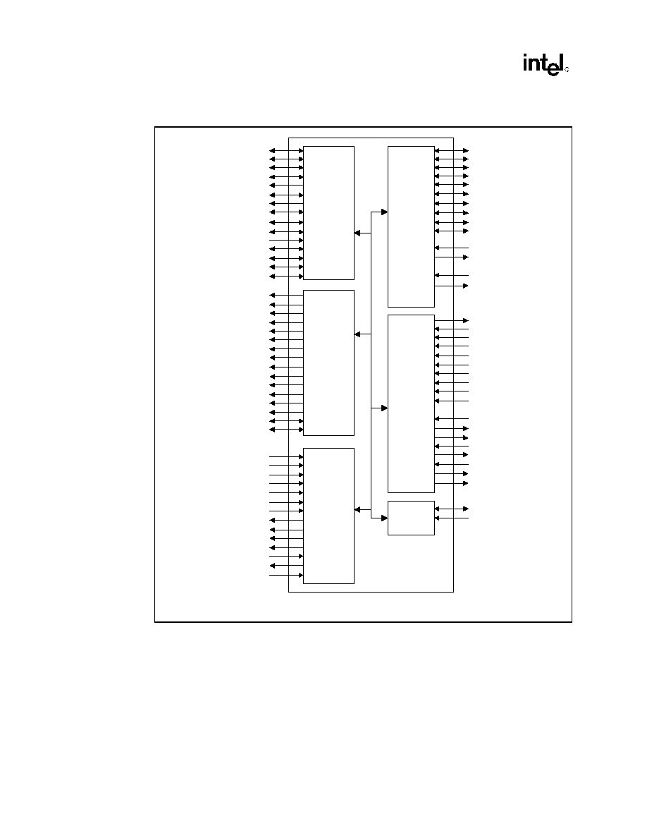
Intel 82443ZX Simplified Block Diagram
BX_BLK.VSD
Host
Interface
A[31:3]#
ADS#
BPRI#
BNR#
CPURST#
DBSY#
DEFER#
HD[63:0]#
HIT#
HITM#
HLOCK#
HREQ[4:0]#
HTRDY#
DRDY#
RS[2:0]#
DRAM
Interface
RASA[5:0]/CSA[5:0]#
RASB[5:0]/CSB[5:0]#
CKE[3:2]/CSA[7:6]#
CKE[5:4]/CSB[7:6]#
CASA[7:0]/DQMA[7:0]
CASB[5,1]/DQMB[5,1]
GCKE/CKE1
SRAS[B,A]#
CKE0/FENA
SCAS[B,A]#
MAA[13:0]
MAB[13,12#,11#,10,9#:0#]
WEA#
WEB#
MD[63:0]
MECC[7:0]
HCLKIN
PCLKIN
GTLREF[B:A]
AGPREF
VTT[B:A]
REF5V
PCIRST#
CRESET#
BREQ0#
TESTIN#
GCLKO
GCLKIN
DCLKO
DCLKWR
AD[31:0]
C/BE[3:0]#
FRAME#
TRDY#
IRDY#
DEVSEL#
PAR
SERR#
PLOCK#
STOP#
PHOLD#
PHLDA#
PREQ[3:0]#
PGNT[3:0]#
GAD[31:0]
GC/BE[3:0]#
GFRAME#
GIRDY#
GTRDY#
GSTOP#
GDEVSEL#
GREQ#
GGNT#
GPAR
PIPE#
SBA[7:0]
RBF#
STOP#
ST[2:0]
ADSTB_A
ADSTB_B
SBSTB
CLKRUN#
BXPWROK
PCI Bus
Interface
(PCI #0)
Clocks,
Reset,
Test,
and
Misc.
AGP
Interface
Power
Mgnt

82443ZX Host Bridge
Datasheet
v
Contents
1
Architectural Overview ...............................................................................................1-1
2
Signal Description ......................................................................................................2-1
2.1
Host Interface Signals...................................................................................2-1
2.2
DRAM Interface ............................................................................................2-3
2.3
PCI Interface (Primary) .................................................................................2-5
2.4
Primary PCI Sideband Interface ...................................................................2-6
2.5
AGP Interface Signals...................................................................................2-7
2.6
Clocks, Reset, and Miscellaneous ................................................................2-9
2.7
Power-Up/Reset Strap Options...................................................................2-10
3
Register Description...................................................................................................3-1
3.1
I/O Mapped Registers ...................................................................................3-2
3.1.1
CONFADD--Configuration Address Register..................................3-2
3.1.2
CONFDATA--Configuration Data Register .....................................3-3
3.1.3
PM2_CTL--ACPI Power Control 2 Control Register .......................3-4
3.2
PCI Configuration Space Access..................................................................3-4
3.2.1
Configuration Space Mechanism Overview .....................................3-5
3.2.2
Routing the Configuration Accesses to PCI or AGP ........................3-5
3.2.3
PCI Bus Configuration Mechanism Overview ..................................3-6
3.2.3.1 Type 0 Access ....................................................................3-6
3.2.3.2 Type 1 Access ....................................................................3-6
3.2.4
AGP Bus Configuration Mechanism Overview ................................3-6
3.2.5
Mapping of Configuration Cycles on AGP .......................................3-7
3.3
Host-to-PCI Bridge Registers (Device 0) ......................................................3-8
3.3.1
VID--Vendor Identification Register (Device 0).............................3-10
3.3.2
DID--Device Identification Register (Device 0) .............................3-10
3.3.3
PCICMD--PCI Command Register (Device 0) ..............................3-11
3.3.4
PCISTS--PCI Status Register (Device 0) .....................................3-12
3.3.5
RID--Revision Identification Register (Device 0) ..........................3-13
3.3.6
SUBC--Sub-Class Code Register (Device 0) ...............................3-13
3.3.7
BCC--Base Class Code Register (Device 0) ................................3-13
3.3.8
MLT--Master Latency Timer Register (Device 0)..........................3-14
3.3.9
HDR--Header Type Register (Device 0) .......................................3-14
3.3.10 APBASE--Aperture Base Configuration Register (Device 0)........3-14
3.3.11 SVID--Subsystem Vendor Identification Register (Device 0)........3-15
3.3.12 SID--Subsystem Identification Register (Device 0).......................3-16
3.3.13 CAPPTR--Capabilities Pointer Register (Device 0) ......................3-16
3.3.14 NBXCFG--NBX Configuration Register (Device 0) .......................3-16
3.3.15 DRAMC--DRAM Control Register (Device 0) ...............................3-19
3.3.16 DRAMT--DRAM Timing Register (Device 0) ................................3-20
3.3.17 PAM[6:0]--Programmable Attribute Map Registers
(Device 0)3-20
3.3.18 DRB[0:7]--DRAM Row Boundary Registers (Device 0) ................3-22
3.3.19 FDHC--Fixed DRAM Hole Control Register (Device 0) ................3-24
3.3.20 MBSC--Memory Buffer Strength Control Register
(Device 0).......................................................................................3-25


