PRELIMINARY
COPYRIGHT © INTEL CORPORATION, 1997
January 1997
Order Number: 272748-003
80296SA COMMERCIAL
CHMOS 16-BIT MICROCONTROLLER
The 80296SA is a member of Intel's 16-bit MCS
Æ
96 microcontroller family. The 80296SA features 6 Mbytes
of linear address space, a demultiplexed bus, and a chip-select unit. The external bus can dynamically switch
between multiplexed and demultiplexed operation. The device has hardware and instructions to support
various digital signal processing algorithms.
NOTE
This datasheet contains information on new products in production. The specifications
are subject to change without notice. Verify with your local Intel sales office that you have
the latest datasheet before finalizing a design.
s
50 MHz Operation
s
6 Mbytes of Linear Address Space
s
512 Bytes of Register RAM
s
2 Kbytes of Code/Data RAM
s
Register-register Architecture
s
Footprint and Functionally Compatible
Upgrade for the 8XC196NP and
80C196NU
s
Optional Phase-locked Loop (PLL)
Circuitry with 2x or 4x Clock Multiplier
s
32 I/O Port Pins
s
19 Interrupt Sources, 14 with
Programmable Priorities
s
4 External Interrupt Pins and NMI Pin
s
2 Flexible 16-bit Timer/Counters with
Quadrature Counting Capability
s
3 Pulse-width Modulator (PWM)
Outputs with High Drive Capability
s
Full-duplex Serial Port with Dedicated
Baud-rate Generator
40 MHz standard; 50 MHz is Speed Premium
s
Chip-select Unit
-- 6 Chip-select Pins
-- Dynamic Demultiplexed/Multiplexed
Address/Data Bus for Each
Chip Select
-- Programmable Wait States
(0≠15) for Each Chip Select
-- Programmable Bus Width
(8- or 16-bit) for Each Chip Select
-- Programmable Address Range for
Each Chip Select
s
Event Processor Array (EPA) with
4 High-speed Capture/Compare
Channels
s
Multiply and Accumulate Executes in
80 ns Using the 40-bit Hardware
Accumulator
s
880 ns 32/16 Unsigned Division
s
100-pin QFP Package
s
Complete System Development
Support
s
High-speed CHMOS Technology

Information in this document is provided in connection with Intel products. No license, express or implied, by
estoppel or otherwise, to any intellectual property rights is granted by this document. Except as provided in
Intel's Terms and Conditions of Sale for such products, Intel assumes no liability whatsoever, and Intel dis-
claims any express or implied warranty, relating to sale and/or use of Intel products including liability or war-
ranties relating to fitness for a particular purpose, merchantability, or infringement of any patent, copyright or
other intellectual property right. Intel products are not intended for use in medical, life saving, or life sustaining
applications.
Intel retains the right to make changes to specifications and product descriptions at any time, without notice.
*Third-party brands and names are the property of their respective owners.
Copies of documents which have an ordering number and are referenced in this document, or other Intel liter-
ature, may be obtained from:
Intel Corporation
P.O. Box 7641
Mt. Prospect, IL 60056-7641
or call 1-800-548-4725

PRELIMINARY
iii
CONTENTS
80296SA Commercial
CHMOS 16-bit Microcontroller
1.0
Product Overview ................................................................................................................ 1
2.0
Nomenclature Overview ...................................................................................................... 2
3.0
Pinout .................................................................................................................................. 3
4.0
Signals ................................................................................................................................ 6
5.0
Address Map ..................................................................................................................... 13
6.0
Electrical Characteristics ................................................................................................... 14
6.1
DC Characteristics........................................................................................................ 14
6.2
AC Characteristics........................................................................................................ 18
6.2.1
Relationship of XTAL1 to CLKOUT ....................................................................... 18
6.2.2
Explanation of AC Symbols ................................................................................... 19
6.2.3
AC Characteristics -- Multiplexed Bus Mode ........................................................ 20
6.2.3.1
System Bus Timings, Multiplexed Bus ...................................................... 22
6.2.3.2
READY Timing, Multiplexed Bus ............................................................... 23
6.2.4
AC Characteristics -- Demultiplexed Bus Mode ................................................... 24
6.2.4.1
System Bus Timings, Demultiplexed Bus .................................................. 26
6.2.4.2
READY Timing, Demultiplexed Bus .......................................................... 27
6.2.4.3
80296SA Deferred Bus Timing Mode ........................................................ 28
6.2.5
HOLD#, HLDA# Timings ....................................................................................... 29
6.2.6
AC Characteristics -- Serial Port, Synchronous Mode 0 ...................................... 30
6.2.7
External Clock Drive .............................................................................................. 31
7.0
Thermal Characteristics .................................................................................................... 33
8.0
80296SA Errata................................................................................................................. 33
9.0
Datasheet Revision History ............................................................................................... 33
FIGURES
1.
80296SA Block Diagram ......................................................................................................1
2.
The 80296SA Family Nomenclature ....................................................................................2
3.
80296SA 100-pin QFP Package ..........................................................................................3
4.
I
CC
versus Frequency in Reset ........................................................................................... 17
5.
Effect of Clock Mode on CLKOUT...................................................................................... 18
6.
System Bus Timings, Multiplexed Bus Mode ..................................................................... 22
7.
Example READY Timings at 50 MHz, Multiplexed Bus, BUSCON
x = 1 Wait State........... 23
8.
System Bus Timings, Demultiplexed Bus Mode................................................................. 26
9.
Example READY Timings at 50 MHz, Demultiplexed Bus, BUSCON
x = 1 Wait State ...... 27
10.
Deferred Bus Mode Timing Diagram.................................................................................. 28
11.
HOLD#, HLDA# Timing Diagram ....................................................................................... 29
12.
Serial Port Waveform -- Synchronous Mode 0.................................................................. 30
13.
External Clock Drive Waveforms........................................................................................ 31
14.
AC Testing Input and Output Waveforms During 5.0 Volt Testing ..................................... 32
15.
Float Waveforms During 5.0 Volt Testing........................................................................... 32

iv
PRELIMINARY
CONTENTS
TABLES
1.
Description of Product Nomenclature .................................................................................. 2
2.
80296SA 100-pin QFP Pin Assignment ............................................................................... 4
3.
80296SA 100-pin QFP Pin Assignment Arranged by Functional Categories ...................... 5
4.
Signal Descriptions .............................................................................................................. 6
5.
80296SA Address Map ...................................................................................................... 13
6.
DC Characteristics Over Specified Operating Conditions .................................................. 14
7.
AC Timing Symbol Definitions............................................................................................ 19
8.
AC Characteristics the 80C296SA Will Meet, Multiplexed Bus Mode ................................ 20
9.
AC Characteristics the External Memory System Must Meet, Multiplexed Bus Mode ....... 21
10.
AC Characteristics the 80C296SA Will Meet, Demultiplexed Bus Mode ........................... 24
11.
AC Characteristics the External Memory System Must Meet, Demultiplexed Bus Mode .. 25
12.
HOLD#, HLDA# Timings .................................................................................................... 29
13.
Serial Port Timing -- Synchronous Mode 0 ....................................................................... 30
14.
External Clock Drive........................................................................................................... 31
15.
Thermal Characteristics ..................................................................................................... 33

PRELIMINARY
1
80296SA COMMERCIAL CHMOS 16-BIT MICROCONTROLLER
1.0
PRODUCT OVERVIEW
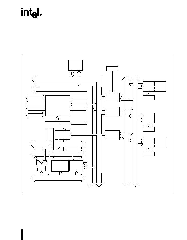
The 80296SA is a member of Intel's 16-bit MCS
Æ
96 microcontroller family. The 80296SA features 6 Mbytes
of linear address space, a demultiplexed bus, and a chip-select unit. The external bus can dynamically switch
between multiplexed and demultiplexed operation. The device has hardware and instructions to support
various digital signal processing algorithms.
Figure 1. 80296SA Block Diagram
Code/Data
RAM
(2 Kbytes)
Port 3
Bus Control Signals
A19:16
AD15:0
Memory Data Bus (16)
SIO
Baud-
rate
Generator
EPA
Timer 1
Timer 2
Port 1
Port 4
PWM
Port 2
Source 2 Addr (24)
Source 2 Data (16)
Bus
Controller
A15:0
Source 1 Addr (24)
Source 1 Data (16)
Destination Addr (24)
Destination Data (16)
A3175-02
Aligner
Chip-select
Unit
Peripheral
Bus
Interface
Memory
Interface
Unit
Register File
(3-port RAM)
Instruction
Sequencer
Queue
ALU
Interrupt
Controller
Memory Data Bus (16)
Memory Addr Bus (24)
Memory Addr Bus (24)
Peripheral Addr Bus (8)
Peripheral Data Bus (16)


