
© INTEL CORPORATION, 1997
September, 1997
Order Number: 273123-001
80960MC
EMBEDDED 32-BIT MICROPROCESSOR
WITH INTEGRATED FLOATING-POINT UNIT
AND MEMORY MANAGEMENT UNIT
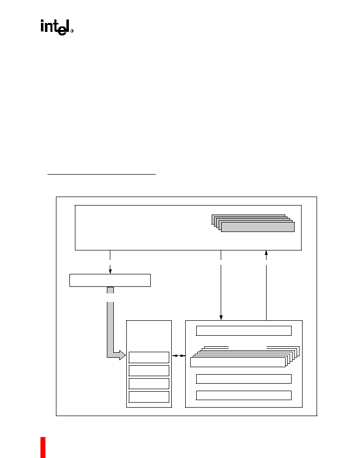
Figure 1. The 80960MC Processor's Highly Parallel Architecture
Commercial
s
High-Performance Embedded Architecture
-- 25 MIPS Burst Execution at 25 MHz
-- 9.4 MIPS* Sustained Execution at
25 MHz
s
On-Chip Floating Point Unit
-- Supports IEEE 754 Floating Point
Standard
-- Full Transcendental Support
-- Four 80-Bit Registers
-- 13.6 Million Whetstones/s
(Single Precision) at 25 MHz
s
512-Byte On-Chip Instruction Cache
-- Direct Mapped
-- Parallel Load/Decode for Uncached
Instructions
s
Multiple Register Sets
-- Sixteen Global 32-Bit Registers
-- Sixteen Local 32-Bit Registers
-- Four Local Register Sets Stored
On-Chip (Sixteen 32-Bit Registers per
Set)
-- Register Scoreboarding
s
On-Chip Memory Management Unit
-- 4 Gbyte Virtual Address Space per
Task
-- 4 Kbyte Pages with Supervisor/User
Protection
s
Built-in Interrupt Controller
-- 32 Priority Levels
-- 248 Vectors
-- Supports M8259A
-- 3.4
µ
s Latency @ 25 MHz
s
Easy to Use, High Bandwidth 32-Bit Bus
-- 66.7 Mbytes/s Burst
-- Up to 16 Bytes Transferred per Burst
s
Multitasking and Multiprocessor Support
-- Automatic Task dispatching
-- Prioritized Task Queues
s
Advanced Package Technology
-- 132-Lead Ceramic Pin Grid Array
SIXTEEN
32-BIT GLOBAL
REGISTERS
64- BY 32-BIT
LOCAL
REGISTER
CACHE
32-BIT
INSTRUCTION
EXECUTION
UNIT
INSTRUCTION
FETCH UNIT
512-BYTE
INSTRUCTION
CACHE
INSTRUCTION
DECODER
MICRO-
INSTRUCTION
SEQUENCER
MICRO-
INSTRUCTION
ROM
32-BIT
BUS CONTROL
LOGIC
32-BIT
BURST
BUS
FOUR
80-BIT FP
REGISTERS
80-BIT
FPU
MMU

Information in this document is provided in connection with Intel products. No license, express or implied, by
estoppel or otherwise, to any intellectual property rights is granted by this document. Except as provided in
Intel's Terms and Conditions of Sale for such products, Intel assumes no liability whatsoever, and Intel
disclaims any express or implied warranty, relating to sale and/or use of Intel products including liability or
warranties relating to fitness for a particular purpose, merchantability, or infringement of any patent, copyright
or other intellectual property right. Intel products are not intended for use in medical, life saving, or life
sustaining applications. Intel may make changes to specifications and product descriptions at any time, without
notice. Contact your local Intel sales office or your distributor to obtain the latest specifications and before
placing your product order.
Intel retains the right to make changes to specifications and product descriptions at any time, without notice.
*Third party brands and names are the property of their respective owners.
Copies of documents which have an ordering number and are referenced in this document, or other Intel
literature, may be obtained from:
Intel Corporation
P.O. Box 7641
Mt. Prospect IL 60056-7641
or call 1-800-879-4683
Many documents are available for download from Intel's website at http://www.intel.com
Copyright © Intel Corporation 1997

80960MC
iii
1.0 THE i960
Æ
MC PROCESSOR ................................................................................................................. .. 1
1.1 Key Performance Features ................................................................................................................. 2
1.1.1 Memory Space And Addressing Modes ................................................................................... 4
1.1.2 Data Types ............................................................................................................. .................. 4
1.1.3 Large Register Set ..................................................................................................... .............. 4
1.1.4 Multiple Register Sets .............................................................................................................. 5
1.1.5 Instruction Cache ..................................................................................................................... 5
1.1.6 Register Scoreboarding ................................................................................................. .......... 5
1.1.7 Memory Management and Protection ...................................................................................... 6
1.1.8 Floating-Point Arithmetic .............................................................................................. ............ 6
1.1.9 Multitasking Support ................................................................................................................ 7
1.1.10 Synchronization and Communication .................................................................................... 7
1.1.11 High Bandwidth Local Bus ..................................................................................................... 7
1.1.12 Multiple Processor Support .................................................................................................... 7
1.1.13 Interrupt Handling .................................................................................................... .............. 8
1.1.14 Debug Features ..................................................................................................................... 8
1.1.15 Fault Detection ....................................................................................................................... 8
1.1.16 Inter-Agent Communications (IAC) ...................................................................................... .. 9
1.1.17 Built-in Testability ................................................................................................................... 9
1.1.18 Compatibility with 80960K-Series ...................................................................................... .... 9
1.1.19 CHMOS ................................................................................................................. ................. 9
2.0 ELECTRICAL SPECIFICATIONS ................................................................................................ ........... 13
2.1 Power and Grounding ...................................................................................................... ................. 13
2.2 Power Decoupling Recommendations ......................................................................................... .... 13
2.3 Connection Recommendations ........................................................................................................ 13
2.4 Characteristic Curves ....................................................................................................................... 13
2.5 Test Load Circuit .............................................................................................................................. 16
2.7 DC Characteristics ....................................................................................................... ..................... 17
2.6 Absolute Maximum Ratings .............................................................................................................. 17
2.8 AC Specifications ............................................................................................................................. 18
2.9 Design Considerations ..................................................................................................................... 22
3.0 MECHANICAL DATA .............................................................................................................................. 22
3.1 Packaging ......................................................................................................................................... 22
3.1.1 Pin Assignment ...................................................................................................................... 22
3.2 Pinout ............................................................................................................................................... 26
3.3 Package Thermal Specification ........................................................................................................ 28
4.0 WAVEFORMS ......................................................................................................................................... 30
5.0 REVISION HISTORY ............................................................................................................................... 35

80960MC
iv
FIGURES
Figure 1.
80960MC Programming Environment ........................................................................................ 1
Figure 2.
Instruction Formats .................................................................................................................... 4
Figure 3.
Multiple Register Sets Are Stored On-Chip ............................................................................... 6
Figure 4.
Connection Recommendations for Low Current Drive Network .............................................. 13
Figure 5.
Connection Recommendations for High Current Drive Network .............................................. 13
Figure 6.
Typical Supply Current vs. Case Temperature ........................................................................ 14
Figure 7.
Typical Current vs. Frequency (Room Temp) .......................................................................... 14
Figure 8.
Typical Current vs. Frequency (Hot Temp) .............................................................................. 15
Figure 9.
Worst-Case Voltage vs. Output Current on Open-Drain Pins .................................................. 15
Figure 10.
Capacitive Derating Curve ....................................................................................................... 15
Figure 11.
Test Load Circuit for Three-State Output Pins ......................................................................... 16
Figure 12.
Test Load Circuit for Open-Drain Output Pins ......................................................................... 16
Figure 13.
Drive Levels and Timing Relationships for 80960MC Signals ................................................. 18
Figure 14.
Timing Relationship of L-Bus Signals ................................................................................ ...... 19
Figure 15.
System and Processor Clock Relationship ............................................................................. . 19
Figure 16.
Processor Clock Pulse (CLK2) ................................................................................................ 21
Figure 17.
RESET Signal Timing .............................................................................................................. 21
Figure 18.
HOLD Timing ........................................................................................................................... 22
Figure 19.
132-Lead Pin-Grid Array (PGA) Package ................................................................................ 23
Figure 20.
80960MC PGA Pinout--View from Bottom (Pins Facing Up) .................................................. 24
Figure 21.
80960MC PGA Pinout--View from Top (Pins Facing Down) .................................................. 25
Figure 22.
25 MHz Maximum Allowable Ambient Temperature ................................................................ 29
Figure 23.
Non-Burst Read and Write Transactions Without Wait States ................................................. 30
Figure 24.
Burst Read and Write Transaction Without Wait States .......................................................... 31
Figure 25.
Burst Write Transaction with 2, 1, 1, 1 Wait States .................................................................. 32
Figure 26.
Accesses Generated by Quad Word Read Bus Request, Misaligned Two Bytes from
Quad Word Boundary (1, 0, 0, 0 Wait States) ......................................................................... 33
Figure 27.
Interrupt Acknowledge Transaction ......................................................................................... 34
Figure 28.
Bus Exchange Transaction (PBM = Primary Bus Master, SBM = Secondary Bus Master) ..... 35
TABLES
Table 1.
80960MC Instruction Set ........................................................................................................... 3
Table 2.
Memory Addressing Modes ....................................................................................................... 4
Table 3.
Sample Floating-Point Execution Times (µs) at 25 MHz ........................................................... 7
Table 4.
80960MC Pin Description: L-Bus Signals .................................................................................. 9
Table 5.
80960MC Pin Description: Support Signals ............................................................................. 11
Table 6.
DC Characteristics ................................................................................................................... 17
Table 7.
80960MC AC Characteristics (25 MHz) ...................................................................................20
Table 8.
80960MC PGA Pinout -- In Pin Order .....................................................................................26
Table 9.
80960MC PGA Pinout -- In Signal Order ................................................................................ 27
Table 10.
80960MC PGA Package Thermal Characteristics ................................................................... 28
1
80960MC
1.0
THE i960
Æ
MC PROCESSOR
The 80960MC, a member of Intel's i960
Æ
32-bit
processor family, is ideally suited for embedded
applications. It includes a 512-byte instruction cache
and a built-in interrupt controller. The 80960MC has
a large register set, multiple parallel execution units
and a high-bandwidth burst bus. Using advanced
RISC technology, this processor is capable of
execution rates in excess of 9.4 million instructions
per second
*
. The 80960MC is well-suited for a wide
range of applications including non-impact printers,
I/O control and specialty instrumentation. The
embedded market includes applications as diverse
as industrial automation, avionics, image
processing, graphics and networking. These types of
applications require high integration, low power
consumption, quick interrupt response times and
* Relative to Digital Equipment Corporation's VAX-11/780*
at 1 MIPS
high performance. Since time to market is critical,
embedded processors must be easy to use in both
hardware and software designs.
All members of the i960 processor family share a
common core architecture which utilizes RISC tech-
nology so that, except for special functions, the
family members are object-code compatible. Each
new processor in the family adds its own special set
of functions to the core to satisfy the needs of a
specific application or range of applications in the
embedded market.
The 80960MC includes an integrated Floating Point
Unit (FPU), a Memory Management Unit (MMU),
multitasking support, and multiprocessor support.
Two commercial members of the i960
Æ
family
provide similar features: the 80960KB processor with
integrated FPU and the 80960KA without floating-
point.
Figure 1. 80960MC Programming Environment
INSTRUCTION CACHE
INSTRUCTION
STREAM
FETCH
LOAD
STORE
SIXTEEN 32-BIT GLOBAL REGISTERS
g0
g15
SIXTEEN 32-BIT LOCAL REGISTERS
REGISTER CACHE
FOUR 80-BIT FLOATING POINT REGISTERS
r0
r15
CONTROL REGISTERS
INSTRUCTION
EXECUTION
INSTRUCTION
POINTER
ARITHMETIC
CONTROLS
PROCESS
CONTROLS
TRACE
CONTROLS
ARCHITECTURALLY
DEFINED
DATA STRUCTURES
FFFF FFFFH
0000 0000H
ADDRESS SPACE
PROCESSOR STATE
REGISTERS

80960MC
2
1.1
Key Performance Features
The 80960 architecture is based on the most recent
advances in microprocessor technology and is
grounded in Intel's long experience in the design and
manufacture of embedded microprocessors. Many
features contribute to the 80960MC's exceptional
performance:
1.
Large Register Set. Having a large number of
registers reduces the number of times that a
processor needs to access memory. Modern
compilers can take advantage of this feature to
optimize execution speed. For maximum flexi-
bility, the 80960MC provides thirty-two 32-bit
registers. (See
Figure 2
.)
2.
Fast Instruction Execution. Simple functions
make up the bulk of instructions in most
programs so that execution speed can be
improved by ensuring that these core instruc-
tions are executed as quickly as possible. The
most frequently executed instructions such as
register-register moves, add/subtract, logical
operations and shifts execute in one to two
cycles. (
Table 1
contains a list of instructions.)
3.
Load/Store Architecture. One way to improve
execution speed is to reduce the number of
times that the processor must access memory
to perform an operation. As with other proces-
sors based on RISC technology, the 80960MC
has a Load/Store architecture. As such, only
the LOAD and STORE instructions reference
memory; all other instructions operate on regis-
ters. This type of architecture simplifies instruc-
tion decoding and is used in combination with
other techniques to increase parallelism.
4.
Simple Instruction Formats. All instructions
in the 80960MC are 32 bits long and must be
aligned on word boundaries. This alignment
makes it possible to eliminate the instruction
alignment stage in the pipeline. To simplify the
instruction decoder, there are only five instruc-
tion formats; each instruction uses only one
format. (See
Figure 3
.)
5.
Overlapped Instruction Execution. Load
operations allow execution of subsequent
instructions to continue before the data has
been returned from memory, so that these
instructions can overlap the load. The
80960MC manages this process transparently
to software through the use of a register score-
board. Conditional instructions also make use
of a scoreboard so that subsequent unrelated
instructions may be executed while the condi-
tional instruction is pending.
6.
Integer Execution Optimization. When the
result of an arithmetic execution is used as an
operand in a subsequent calculation, the value
is sent immediately to its destination register.
Yet at the same time, the value is put on a
bypass path to the ALU, thereby saving the
time that otherwise would be required to
retrieve the value for the next operation.
7.
Bandwidth Optimizations. The 80960MC
gets optimal use of its memory bus bandwidth
because the bus is tuned for use with the on-
chip instruction cache: instruction cache line
size matches the maximum burst size for
instruction fetches. The 80960MC automati-
cally fetches four words in a burst and stores
them directly in the cache. Due to the size of
the cache and the fact that it is continually filled
in anticipation of needed instructions in the
program flow, the 80960MC is relatively insen-
sitive to memory wait states. The benefit is that
the 80960MC delivers outstanding perfor-
mance even with a low cost memory system.
8.
Cache Bypass. When a cache miss occurs,
the processor fetches the needed instruction
then sends it on to the instruction decoder at
the same time it updates the cache. Thus, no
extra time is spent to load and read the cache.

80960MC
3
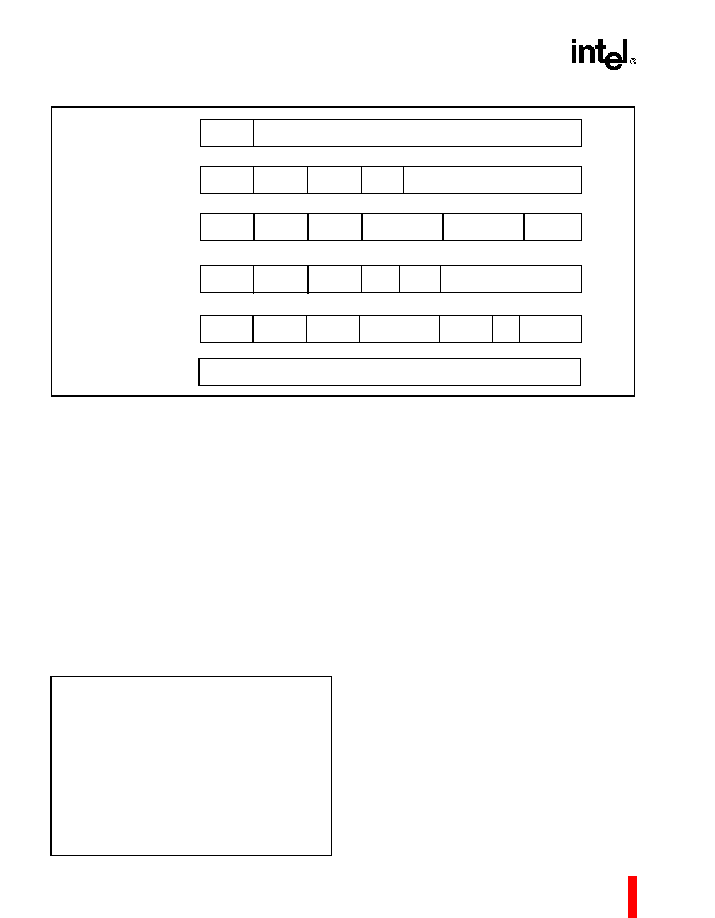
Table 1. 80960MC Instruction Set
Data Movement
Process Management
Floating Point
Logical
Load
Store
Move
Load Address
Load Physical Address
Schedule Process
Saves Process
Resume Process
Load Process Time
Modify Process Controls
Wait
Conditional Wait
Signal
Receive
Conditional Receive
Send
Send Service
Atomic Add
Atomic Modify
Add
Subtract
Multiply
Divide
Remainder
Scale
Round
Square Root
Sine
Cosine
Tangent
Arctangent
Log
Log Binary
Log Natural
Exponent
Classify
Copy Real Extended
Compare
And
Not And
And Not
Or
Exclusive Or
Not Or
Or Not
Nor
Exclusive Nor
Not
Nand
Rotate
Comparison
Branch
Bit and Bit Field
String
Compare
Conditional Compare
Compare and Increment
Compare and Decrement
Unconditional Branch
Conditional Branch
Compare and Branch
Set Bit
Clear Bit
Not Bit
Check Bit
Alter Bit
Scan For Bit
Scan Over Bit
Extract
Modify
Move String
Move Quick String
Fill String
Compare String
Scan Byte for Equal
Conversion
Decimal
Call/Return
Arithmetic
Convert Real to Integer
Convert Integer to Real
Move
Add with Carry
Subtract with Carry
Call
Call Extended
Call System
Return
Branch and Link
Add
Subtract
Multiply
Divide
Remainder
Modulo
Shift
Fault
Debug
Miscellaneous
Conditional Fault
Synchronize Faults
Modify Trace Controls
Mark
Force Mark
Flush Local Registers
Inspect Access
Modify Arithmetic
Controls
Test Condition Code
80960MC
4
Figure 2. Instruction Formats
Opcode
Displacement
Opcode
Reg/Lit
Reg
M
Displacement
Displacement
Control
Compare and
Branch
Register to
Register
Memory Access-
Short
Memory Access-
Long
Opcode
Reg
Reg/Lit
Modes
Ext'd Op
Reg/Lit
Opcode
Reg
Base
M
X
Offset
Opcode
Reg
Base
Mode
Scale
xx
Offset
1.1.1
Memory Space And Addressing Modes
The 80960MC allows each task (process) to address
a logical memory space of up to 4 Gbytes. Each
task's address space is divided into four 1 Gbyte
regions and each region can be mapped to physical
addresses by zero, one, or two levels of page tables.
The region with the highest addresses (Region 3) is
common to all tasks.
In keeping with RISC design principles, the number
of addressing modes is minimal yet includes all
those necessary to ensure efficient execution of
high-level languages such as Ada, C, and Fortran.
Table 2
lists the memory accessing modes.
1.1.2
Data Types
The 80960MC recognizes the following data types:
Numeric:
∑ 8-, 16-, 32- and 64-bit ordinals
∑ 8-, 16-, 32- and 64-bit integers
∑ 32-, 64- and 80-bit real numbers
Non-Numeric:
∑ Bit
∑ Bit Field
∑ Triple Word (96 bits)
∑ Quad-Word (128 bits)
1.1.3
Large Register Set
The 80960MC programming environment includes a
large number of registers. 36 registers are available
at any time; this greatly reduces the number of
memory accesses required to perform algorithms,
which leads to greater instruction processing speed.
Two types of general-purpose registers are avail-
able: local and global. The 20 global registers
consist of sixteen 32-bit registers (G0 though G15)
and four 80-bit registers (FP0 through FP3). These
Table 2. Memory Addressing Modes
∑ 12-Bit Offset
∑ 32-Bit Offset
∑ Register-Indirect
∑ Register + 12-Bit Offset
∑ Register + 32-Bit Offset
∑ Register + (Index-Register x Scale-Factor)
∑ Register x Scale Factor + 32-Bit Displacement
∑ Register + (Index-Register x Scale-Factor) + 32-
Bit Displacement
∑ Scale-Factor is 1, 2, 4, 8 or 16

80960MC
5
registers perform the same function as the general-
purpose registers provided in other popular micro-
processors. The term
global
refers to the fact that
these registers retain their contents across proce-
dure calls.
The local registers are procedure-specific. For each
procedure call, the 80960MC allocates 16 local
registers (R0 through R15). Each local register is 32
bits wide. Any register can also be used for floating-
point operations; the 80-bit floating-point registers
are provided for extended precision.
1.1.4
Multiple Register Sets
To further increase the efficiency of the register set,
multiple sets of local registers are stored on-chip
(See
Figure 4
). This cache holds up to four local
register frames, which means that up to three proce-
dure calls can be made without having to access the
procedure stack resident in memory.
Although programs may have procedure calls nested
many calls deep, a program typically oscillates back
and forth between only two to three levels. As a
result, with four stack frames in the cache, the prob-
ability of having a free frame available on the cache
when a call is made is very high. Runs of representa-
tive C-language programs show that 80% of the calls
are handled without needing to access memory.
When four or more procedures are active and a new
procedure is called, the 80960MC moves the oldest
local register set in the stack-frame cache to a
procedure stack in memory to make room for a new
set of registers. Global register G15 is the frame
pointer (FP) to the procedure stack.
Global registers are not exchanged on a procedure
call, but retain their contents, making them available
to all procedures for fast parameter passing.
1.1.5
Instruction Cache
To further reduce memory accesses, the 80960MC
includes a 512-byte on-chip instruction cache. The
instruction cache is based on the concept of
locality
of reference
; most programs are typically not
executed in a steady stream but consist of many
branches, loops and procedure calls that lead to
jumping back and forth in the same small section of
code. Thus, by maintaining a block of instructions in
cache, the number of memory references required to
read instructions into the processor is greatly
reduced.
To load the instruction cache, instructions are
fetched in 16-byte blocks; up to four instructions can
be fetched at one time. An efficient prefetch algo-
rithm increases the probability that an instruction is
already in the cache when it is needed.
Code for small loops often fits entirely within the
cache, leading to an increase in processing speed
since further memory references might not be
necessary until the program exits the loop. Similarly,
when calling short procedures, the code for the
calling procedure is likely to remain in the cache so it
is there on the procedure's return.
1.1.6
Register Scoreboarding
The instruction decoder is optimized in several ways.
One optimization method is the ability to overlap
instructions by using
register scoreboarding
.
Register scoreboarding occurs when a LOAD moves
a variable from memory into a register. When the
instruction initiates, a scoreboard bit on the target
register is set. Once the register is loaded, the bit is
reset. In between, any reference to the register
contents is accompanied by a test of the scoreboard
bit to ensure that the load has completed before
processing continues. Since the processor does not
need to wait for the LOAD to complete, it can
execute additional instructions placed between the
LOAD and the instruction that uses the register
contents, as shown in the following example:
ld data_2, r4
ld data_2, r5
Unrelated instruction
Unrelated instruction
add R4, R5, R6
In essence, the two unrelated instructions between
LOAD and ADD are executed "for free" (i.e., take no
apparent time to execute) because they are
executed while the register is being loaded. Up to
three load instructions can be pending at one time
with three corresponding scoreboard bits set. By
exploiting this feature, system programmers and
compiler writers have a useful tool for optimizing
execution speed.
80960MC
6
Figure 3. Multiple Register Sets Are Stored On-Chip
REGISTER
CACHE
ONE OF FOUR
LOCAL
REGISTER SETS
LOCAL REGISTER SET
R
15
R
0
31
0
1.1.7
Memory Management and Protection
The 80960MC is ideal for multitasking applications
that require software protection and a large address
space. To ensure the highest level of performance
possible, the memory management unit (MMU) and
translation look-aside buffer (TLB) are contained on-
chip.
The 80960MC supports a conventional form of
demand-paged virtual memory in which the address
space is divided into 4-Kbyte pages. Studies indicate
that a 4-Kbyte page is the optimum size for a broad
range of applications.
Each page table entry includes a 2-bit page rights
field that specifies whether the page is a no-access,
read-only, or read-write page. This field is inter-
preted differently depending on whether the current
task (process) is executing in user or supervisor
mode, as shown below:
Rights User
Supervisor
00
No Access
Read-Only
01
No Access
Read-Write
10
Read-Only
Read-Write
11
Read-Write
Read-Write
1.1.8
Floating-Point Arithmetic
In the 80960MC, floating-point arithmetic is an
integral part of the architecture. Having the floating-
point unit integrated on-chip provides two advan-
tages. First, it improves the performance of the chip
for floating-point applications, since no additional
bus overhead is associated with floating-point calcu-
lations, thereby leaving more time for other bus oper-
ations such as I/O. Second, the cost of using
floating-point operations is reduced because a
separate coprocessor chip is not required.
The 80960MC floating-point (real-number) data
types include single-precision (32-bit), double-preci-
sion (64-bit) and extended precision (80-bit) floating-
point numbers. Any registers may be used to
execute floating-point operations.
The processor provides hardware support for both
mandatory and recommended portions of IEEE
Standard 754 for floating-point arithmetic, including
all arithmetic, exponential, logarithmic and other
transcendental functions.
Table 3
shows execution
times for some representative instructions.

80960MC
7
1.1.9
Multitasking Support
Multitasking programs commonly involve the moni-
toring and control of an external operation, such as
the activities of a process controller or the move-
ments of a machine tool. These programs generally
consist of a number of processes that run indepen-
dently of one another, but share a common
database or pass data among themselves.
The 80960MC offers several hardware functions
designed to support multitasking systems. One
unique feature, called self-dispatching, allows a
processor to switch itself automatically among
scheduled tasks. When self-dispatching is used, all
the operating system is required to do is place the
task in the scheduling queue.
When the processor becomes available, it
dispatches the task from the beginning of the queue
and then executes it until it becomes blocked, inter-
rupted, or until its time-slice expires. It then returns
the task to the end of the queue (i.e., automatically
reschedules it) and dispatches the next ready task.
During these operations, no communication between
the processor and the operating system is necessary
until the running task is complete or an interrupt is
issued.
1.1.10 Synchronization and Communication
The 80960MC also offers instructions to set up and
test semaphores to ensure that concurrent tasks
remain synchronized and no data inconsistency
results. Special data structures, known as communi-
cation ports, provide the means for exchanging
parameters and data structures. Transmission of
information by means of communication ports is
asynchronous and automatically buffered by the
processor.
Communication between tasks by means of ports
can be carried out independently of the operating
system. Once the ports have been set up by the
programmer, the processor handles the message
passing automatically.
1.1.11 High Bandwidth Local Bus
The 80960MC CPU resides on a high-bandwidth
address/data bus known as the local bus (L-Bus).
The L-Bus provides a direct communication path
between the processor and the memory and I/O
subsystem interfaces. The processor uses the L-Bus
to fetch instructions, manipulate memory and
respond to interrupts. L-Bus features include:
∑ 32-bit multiplexed address/data path
∑ Four-word burst capability which allows transfers
from 1 to 16 bytes at a time
∑ High bandwidth reads and writes with 66.7
MBytes/s burst (at 25 MHz)
∑ Special signal to indicate whether a memory trans-
action can be cached
Table 4
defines L-bus signal names and functions;
Table 5
defines other component-support signals
such as interrupt lines.
1.1.12 Multiple Processor Support
One means of increasing the processing power of a
system is to run two or more processors in parallel.
Since microprocessors are not generally designed to
run in tandem with other processors, designing such
a system is usually difficult and costly.
The 80960MC solves this problem by offering a
number of functions to coordinate the actions of
multiple processors. First, messages can be passed
between processors to initiate actions such as
flushing a cache, stopping or starting another
processor, or preempting a task. The messages are
passed on the bus and allow multiple processors to
run together smoothly, with rare need to lock the bus
or memory.
Table 3. Sample Floating-Point Execution Times
(µs) at 25 MHz
Function
32-Bit
64-Bit
Add
0.4
0.5
Subtract
0.4
0.5
Multiply
0.7
1.3
Divide
1.3
2.9
Square Root
3.7
3.9
Arctangent
10.1
13.1
Exponent
11.3
12.5
Sine
15.2
16.6
Cosine
15.2
16.6

80960MC
8
Second, a set of synchronization instructions help
maintain memory coherency. These instructions
permit several processors to modify memory at the
same time without inserting inaccuracies or ambigu-
ities into shared data structures.
The self-dispatching mechanism -- in addition to
being used in single-processor systems -- provides
the means to increase the performance of a system
merely by adding processors. Each processor can
either work on the same pool of tasks (sharing the
same queue with other processors) or can be
restricted to its own queue.
When processors perform system operation, they
synchronize themselves by using atomic operations
and sending special messages between each other.
In theory, changing the number of processors in a
system does not require a software change.
Software executes correctly regardless of the
number of processors in the system; systems with
more processors simply execute faster.
1.1.13 Interrupt Handling
The 80960MC can be interrupted in two ways: by the
activation of one of four interrupt pins or by sending
a message on the processor's data bus.
The 80960MC is unusual in that it automatically
handles interrupts on a priority basis and can keep
track of pending interrupts through its on-chip inter-
rupt controller. Two of the interrupt pins can be
configured to provide 8259A-style handshaking for
expansion beyond four interrupt lines.
An interrupt message is made up of a vector number
and an interrupt priority. When the interrupt priority is
greater than that of the currently running task, the
processor accepts the interrupt and uses the vector
as an index into the interrupt table. When the priority
of the interrupt message is below that of the current
task, the processor saves the information in a
section of the interrupt table reserved for pending
interrupts.
1.1.14 Debug Features
The 80960MC has built-in debug capabilities,
including two types of breakpoints and six trace
modes. Debug features are controlled by two
internal 32-bit registers: the Process-Controls Word
and the Trace-Controls Word. By setting bits in these
control words, a software debug monitor can closely
control how the processor responds during program
execution.
The 80960MC has both hardware and software
breakpoints. It provides two hardware breakpoint
registers on-chip which, by using a special
command, can be set to any value. When the
instruction pointer matches either breakpoint register
value, the breakpoint handling routine is automati-
cally called.
The 80960MC also provides software breakpoints
through the use of two instructions: MARK and
FMARK. These can be placed at any point in a
program and cause the processor to halt execution
at that point and call the breakpoint handling routine.
The breakpoint mechanism is easy to use and
provides a powerful debugging tool.
Tracing is available for instructions (single step
execution), calls and returns and branching. Each
trace type may be enabled separately by a special
debug instruction. In each case, the 80960MC
executes the instruction first and then calls a trace
handling routine (usually part of a software debug
monitor). Further program execution is halted until
the routine completes, at which time execution
resumes at the next instruction. The 80960MC'S
tracing mechanisms, implemented completely in
hardware, greatly simplify the task of software test
and debug.
1.1.15 Fault Detection
The 80960MC has an automatic mechanism to
handle faults. There are ten fault types include
floating point, trace and arithmetic faults. When the
processor detects a fault, it automatically calls the
appropriate fault handling routine and saves the
current instruction pointer and necessary state infor-
mation to make efficient recovery possible. The
processor posts diagnostic information on the type of
fault to a Fault Record. Like interrupt handling
routines, fault handling routines are usually written to
meet the needs of specific applications and are often
included as part of the operating system or kernel.
For each of the ten fault types, numerous subtypes
provide specific information about a fault. For
example, a floating point fault may have the subtype
set to an Overflow or Zero-Divide fault. The fault
handler can use this specific information to respond
correctly to the fault.

80960MC
9
1.1.16 Inter-Agent Communications (IAC)
To coordinate their actions, processors in a multiple
processor system need a means for communicating
with each other. The 80960MC does this through a
mechanism known as "IACs" -- Inter-Agent Commu-
nication messages.
IAC messages cause a variety of actions including
starting and stopping processors, flushing instruction
caches and TLBs, and sending interrupts to other
processors in the system. The upper 16 Mbytes of
the processor's physical memory space is reserved
for sending and receiving IAC messages.
1.1.17 Built-in Testability
Upon reset, the 80960MC automatically conducts an
exhaustive internal test of its major blocks of logic.
Then, before executing its first instruction, it does a
zero check sum on the first eight words in memory to
ensure that the memory image was programmed
correctly. When a problem is discovered at any point
during the self-test, the 80960MC asserts its
FAILURE pin and does not begin program execu-
tion. Self test takes approximately 47,000 cycles to
complete.
System manufacturers can use the 80960MC's self-
test feature during incoming parts inspection. No
special diagnostic programs need to be written. The
test is both thorough and fast. The self-test capability
helps ensure that defective parts are discovered
before systems are shipped and, once in the field,
the self-test makes it easier to distinguish between
problems caused by processor failure and problems
resulting from other causes.
1.1.18 Compatibility with 80960K-Series
Application programs written for the 80960K-Series
microprocessors can be run on the 80960MC
without modification. The 80960K-Series instruction
set forms the core of the 80960MC's instructions, so
binary compatibility is assured.
1.1.19 CHMOS
The 80960MC is fabricated using Intel's CHMOS IV
(Complementary High Speed Metal Oxide Semicon-
ductor) process. The 80960MC is currently available
at 25 MHz.
Table 4. 80960MC Pin Description: L-Bus Signals (Sheet 1 of 3)
NAME
TYPE
DESCRIPTION
CLK2
I
SYSTEM CLOCK provides the fundamental timing for 80960MC systems. It is
divided by two inside the 80960MC to generate the internal processor clock. Refer
to
Figure 16, Processor Clock Pulse (CLK2) (pg. 21)
LAD31:0
I/O
T.S.
LOCAL ADDRESS / DATA BUS carries 32-bit physical addresses and data to and
from memory. During an address (T
a
) cycle, bits 2-31 contain a physical word
address (bits 0-1 indicate SIZE; see below). During a data (T
d
) cycle, bits 0-31
contain read or write data. These pins float to a high impedance state when not
active.
Bits 0-1 comprise SIZE during a T
a
cycle. SIZE specifies burst transfer size in
words.
LAD1
LAD0
0
0
1 Word
0
1
2 Words
1
0
3 Words
1
1
4 Words
ALE
O
T.S.
ADDRESS LATCH ENABLE indicates the transfer of a physical address. ALE is
asserted during a T
a
cycle and deasserted before the beginning of the T
d
state. It is
active LOW and floats to a high impedance state during a hold cycle (T
h
).
I/O = Input/Output, O = Output, I = Input, O.D. = Open Drain, T.S. = Three-state
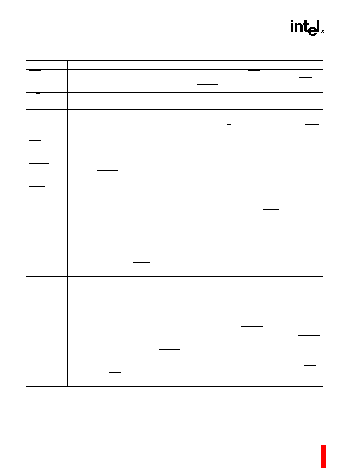
80960MC
10
ADS
O
O.D.
ADDRESS/DATA STATUS indicates an address state. ADS is asserted every T
a
state and deasserted during the following T
d
state. For a burst transaction, ADS is
asserted again every T
d
state where READY was asserted in the previous cycle.
W/R
O
O.D.
WRITE/READ specifies, during a T
a
cycle, whether the operation is a write or read.
It is latched on-chip and remains valid during T
d
cycles.
DT/R
O
O.D.
DATA TRANSMIT / RECEIVE indicates the direction of data transfer to and from
the L-Bus. It is low during T
a
and T
d
cycles for a read or interrupt acknowledgment;
it is high during T
a
and T
d
cycles for a write. DT/R never changes state when DEN
is asserted.
DEN
O
O.D.
DATA ENABLE (active low) enables data transceivers. The processor asserts
DEN# during all T
d
and T
w
states. The DEN# line is an open drain-output of the
80960MC.
READY
I
READY indicates that data on LAD lines can be sampled or removed. When
READY is not asserted during a T
d
cycle, the T
d
cycle is extended to the next cycle
by inserting a wait state (T
w
) and ADS is not asserted in the next cycle.
LOCK
I/O
O.D.
BUS LOCK prevents bus masters from gaining control of the L-Bus during
Read/Modify/Write (RMW) cycles. The processor or any bus agent may assert
LOCK.
At the start of a RMW operation, the processor examines the LOCK pin. When the
pin is already asserted, the processor waits until it is not asserted. When the pin is
not asserted, the processor asserts LOCK during the T
a
cycle of the read trans-
action. The processor deasserts LOCK in the T
a
cycle of the write transaction.
During the time LOCK is asserted, a bus agent can perform a normal read or write
but not a RMW operation.
The processor also asserts LOCK during interrupt-acknowledge transactions.
Do not leave LOCK unconnected. It must be pulled high for the processor to
function properly.
BE3:0
O
O.D.
BYTE ENABLE LINES specify the data bytes (up to four) on the bus which are
used in the current bus cycle. BE3 corresponds to LAD31:24; BE0 corresponds to
LAD7:0.
The byte enables are provided in advance of data:
Byte enables asserted during T
a
specify the bytes of the first data word.
Byte enables asserted during T
d
specify the bytes of the next data word, if any (the
word to be transmitted following the next assertion of READY).
Byte enables that occur during T
d
cycles that precede the last assertion of READY
are undefined. Byte enables are latched on-chip and remain constant from one T
d
cycle to the next when READY is not asserted.
For reads, byte enables specify the byte(s) that the processor actually uses. L-Bus
agents are required to assert only adjacent byte enables (e.g., asserting just BE0
and BE2 is not permitted) and are required to assert at least one byte enable.
Address bits A
0
and A
1
can be decoded externally from the byte enables.
Table 4. 80960MC Pin Description: L-Bus Signals (Sheet 2 of 3)
NAME
TYPE
DESCRIPTION
I/O = Input/Output, O = Output, I = Input, O.D. = Open Drain, T.S. = Three-state

80960MC
11
HOLD/
HLDAR
I
HOLD: A request from an external bus master to acquire the bus. When the
processor receives HOLD and grants bus control to another master, it floats its
three-state bus lines and open-drain control lines, asserts HLDA and enters the T
h
state. When HOLD deasserts, the processor deasserts HLDA and enters the T
i
or
T
a
state.
HOLD ACKNOWLEDGE RECEIVED: Indicates that the processor has acquired
the bus. When the processor is initialized as the secondary bus master this input is
interpreted as HLDAR.
Refer to
Figure 18, HOLD Timing (pg. 22)
.
HLDA/
HOLDR
O
T.S.
HOLD ACKNOWLEDGE: Relinquishes control of the bus to another bus master.
When the processor is initialized as the primary bus master this output is
interpreted as HLDA. When HOLD is deasserted, the processor deasserts HLDA
and goes to either the T
i
or T
a
state.
HOLD REQUEST: Indicates a request to acquire the bus. When the processor is
initialized as the secondary bus master this output is interpreted as HOLDR.
Refer to
Figure 18, HOLD Timing (pg. 22)
.
CACHE/
TAG
O
T.S.
CACHE indicates when an access is cacheable during a T
a
cycle. It is not asserted
during any synchronous access, such as a synchronous load or move instruction
used for sending an IAC message. The CACHE signal floats to a high impedance
state when the processor is idle.
TAG is an input/output signal that, during T
d
and T
w
cycles, identifies the contents
of a 32-bit word as either data (TAG = 0) or an access descriptor (TAG = 1).
Table 5. 80960MC Pin Description: Support Signals (Sheet 1 of 2)
NAME
TYPE
DESCRIPTION
BADAC
I
BAD ACCESS, when asserted in the cycle following the one in which the last
READY of a transaction is asserted, indicates that an unrecoverable error has
occurred on the current bus transaction or that a synchronous load/store instruction
has not been acknowledged.
During system reset the BADAC signal is interpreted differently. When the signal is
high, it indicates that this processor will perform system initialization. When low,
another processor in the system will perform system initialization instead.
RESET
I
RESET clears the processor's internal logic and causes it to reinitialize.
During RESET assertion, the input pins are ignored (except for BADAC and
IAC/INT
0
), the three-state output pins are placed in a high impedance state and
other output pins are placed in their non-asserted states.
RESET must be asserted for at least 41 CLK2 cycles for a predictable RESET. The
HIGH to LOW transition of RESET should occur after the rising edge of both CLK2
and the external bus clock and before the next rising edge of CLK2.
Refer to
Figure 17, RESET Signal Timing (pg. 21)
.
I/O = Input/Output, O = Output, I = Input, O.D. = Open Drain, T.S. = Three-state
Table 4. 80960MC Pin Description: L-Bus Signals (Sheet 3 of 3)
NAME
TYPE
DESCRIPTION
I/O = Input/Output, O = Output, I = Input, O.D. = Open Drain, T.S. = Three-state
80960MC
12
FAILURE
O
O.D.
INITIALIZATION FAILURE indicates that the processor did not initialize correctly.
After RESET deasserts and before the first bus transaction begins, FAILURE
asserts while the processor performs a self-test. When the self-test completes
successfully, then FAILURE deasserts. The processor then performs a zero
checksum on the first eight words of memory. When it fails, FAILURE asserts for a
second time and remains asserted. When it passes, system initialization continues
and FAILURE remains deasserted.
IAC/INT
0
LOCAL
PROCESSOR
NUMBER
I
INTERAGENT COMMUNICATION REQUEST/INTERRUPT 0 indicates an IAC
message or an interrupt is pending. The bus interrupt control register determines
how the signal is interpreted. To signal an interrupt or IAC request in a synchronous
system, this pin -- as well as the other interrupt pins -- must be enabled by being
deasserted for at least one bus cycle and then asserted for at least one additional
bus cycle. In an asynchronous system the pin must remain deasserted for at least
two bus cycles and then asserted for at least two more bus cycles.
LOCAL PROCESSOR NUMBER - this signal is interpreted differently during
system reset. When the signal is a high voltage level it indicates that this processor
is a primary bus master (local processor number = 0). When at a low voltage level it
indicates that this processor is a secondary bus master (local processor number
= 1).
INT
1
I
INTERRUPT 1, like INT
0
, provides direct interrupt signaling.
INT
2
/INTR
I
INTERRUPT2/INTERRUPT REQUEST: The interrupt control register determines
how this pin is interpreted. When INT
2
, it has the same interpretation as the INT
0
and INT
1
pins. When INTR, it is used to receive an interrupt request from an
external interrupt controller.
INT
3
/INTA
I/O
O.D.
INTERRUPT3/INTERRUPT ACKNOWLEDGE: The bus interrupt control register
determines how this pin is interpreted. When INT
3
, it has the same interpretation as
the INT
0
, INT1 and INT2 pins. When INTA, it is used as an output to control
interrupt-acknowledge transactions. The INTA output is latched on-chip and
remains valid during T
d
cycles; as an output, it is open-drain.
N.C.
N/A
NOT CONNECTED indicates pins should not be connected. Never connect any pin
marked N.C. as these pins may be reserved for factory use.
Table 5. 80960MC Pin Description: Support Signals (Sheet 2 of 2)
NAME
TYPE
DESCRIPTION
I/O = Input/Output, O = Output, I = Input, O.D. = Open Drain, T.S. = Three-state

80960MC
13
2.0
ELECTRICAL SPECIFICATIONS
2.1
Power and Grounding
The 80960MC is implemented in CHMOS IV tech-
nology and therefore has modest power require-
ments. Its high clock frequency and numerous
output buffers (address/data, control, error and arbi-
tration signals) can cause power surges as multiple
output buffers simultaneously drive new signal
levels. For clean on-chip power distribution, V
CC
and
V
SS
pins separately feed the device's functional
units. Power and ground connections must be made
to all 80960MC power and ground pins. On the
circuit board, all V
cc
pins must be strapped closely
together, preferably on a power plane; all V
ss
pins
should be strapped together, preferably on a ground
plane.
2.2
Power Decoupling
Recommendations
Place a liberal amount of decoupling capacitance
near the 80960MC. When driving the L-bus the
processor can cause transient power surges, partic-
ularly when connected to a large capacitive load.
Low inductance capacitors and interconnects are
recommended for best high frequency electrical
performance. Inductance is reduced by shortening
board traces between the processor and decoupling
capacitors as much as possible.
2.3
Connection Recommendations
For reliable operation, always connect unused inputs
to an appropriate signal level. In particular, when
one or more interrupt lines are not used, they should
be pulled up. No inputs should ever be left floating.
All open-drain outputs require a pull-up device.
While in most cases a simple pull-up resistor is
adequate, a network of pull-up and pull-down resis-
tors biased to a valid V
IH
(
>
3.0 V) and terminated in
the characteristic impedance of the circuit board is
recommended to limit noise and AC power
consumption.
Figure 5
and
Figure 6
show recom-
mended values for the resistor network for low and
high current drive, assuming a characteristic imped-
ance of 100
.
Terminating output signals in this
fashion limits signal swing and reduces AC power
consumption.
NOTE:
Do not connect external logic to pins marked N.C.
Figure 4. Connection Recommendations
for Low Current Drive Network
Figure 5. Connection Recommendations
for High Current Drive Network
2.4
Characteristic Curves
Figure 7
shows typical supply current requirements
over the operating temperature range of the
processor at supply voltage (V
CC
) of 5 V.
Figure 8
and
Figure 9
show the typical power supply current
(I
CC
) that the 80960MC requires at various operating
frequencies when measured at three input voltage
(V
CC
) levels and two temperatures.
For a given output current (I
OL
) the curve in
Figure 10
shows the worst case output low voltage
(V
OL
).
Figure 11
shows the typical capacitive
derating curve for the 80960MC measured from 1.5V
on the system clock (CLK) to 1.5V on the falling
edge and 1.5V on the rising edge of the L-Bus
address/data (LAD) signals.
220
330
Low Drive Network:
V
OH
= 3.0 V
I
OL
= 20.7 mA
V
CC
OPEN-DRAIN OUTPUT
OPEN-DRAIN OUTPUT
180
390
High Drive Network:
V
OH
= 3.4 V
I
OL
= 25.3 mA
V
CC
80960MC
14
Figure 6. Typical Supply Current vs. Case Temperature
Figure 7. Typical Current vs. Frequency (Room Temp)
-60 -40 -20 0
20
40
60
80
100 120 140
V
CC
= 5.0 V
P
O
W
E
R S
U
P
P
L
Y
CURRE
NT
(
m
A
)
CASE TEMPERATURE (∞C)
25 MHz
20 MHz
16 MHz
380
360
340
320
300
280
260
240
220
200
OPERATING FREQUENCY (MHz)
@4.5V
@5.0V
@5.5V
T
Y
P
I
CA
L
S
U
P
P
L
Y
CURRE
NT
(
m
A
)
TEMP = +22∞C
400
380
360
340
320
300
280
260
240
220
200
180
16
20
25
80960MC
15
Figure 8. Typical Current vs. Frequency (Hot Temp)
OPERATING FREQUENCY (MHz)
@4.5V
@5.0V
@5.5V
T
Y
P
I
CA
L
S
U
P
P
L
Y
CURRE
NT
(
m
A
)
TEMP = +22∞C
380
360
340
320
300
280
260
240
220
200
180
16
20
25
160
Figure 9. Worst-Case Voltage vs. Output Current
on Open-Drain Pins
Figure 10. Capacitive Derating Curve
0
10
20
30
40
50
0.8
0.6
0.4
0.2
0.0
OUTPUT LOW CURRENT(mA)
(TEMP = +85∞C, V
CC
= 4.5V)
O
U
T
P
UT
L
O
W VO
L
T
AG
E
(V
)
0
20
40
60
80
100
30
25
20
15
10
CAPACITIVE LOAD(pF)
(TEMP = +85∞C, V
CC
= 4.5V)
5
0
RISING
FALLING
V
A
LID
D
E
LA
Y
(
ns
)
T
H
R
E
E-
ST
AT
E
O
U
T
P
U
T

80960MC
16
2.5
Test Load Circuit
Figure 12
illustrates the load circuit used to test the
80960MC's three-state pins;
Figure 13
shows the
load circuit used to test the open drain outputs. The
open drain test uses an active load circuit in the form
of a matched diode bridge. Since the open-drain
outputs sink current, only the I
OL
legs of the bridge
are necessary and the I
OH
legs are not used. When
the 80960MC driver under test is turned off, the
output pin is pulled up to V
REF
(i.e., V
OH
). Diode D
1
is turned off and the I
OL
current source flows through
diode D
2
.
When the 80960MC open-drain driver under test is
on, diode D
1
is also on and the voltage on the pin
being tested drops to V
OL
. Diode D
2
turns off and I
OL
flows through diode D
1
.
Figure 11. Test Load Circuit for Three-State
Output Pins
Figure 12. Test Load Circuit for Open-Drain
Output Pins
THREE-STATE OUTPUT
C
L
= 50 pF for all signals
C
L
C
L
OPEN-DRAIN OUTPUT
I
OL
D
2
I
OL
Tested at 25 mA
V
REF
= V
CC
D1 and D
2
are matched
D
1
C
L
= 50 pF for all signals

80960MC
17
2.7
DC Characteristics
2.6
Absolute Maximum Ratings
NOTICE: This is a production data sheet. The specifi-
cations are subject to change without notice.
Operating Temperature (PGA) ...... 0∞ C to +85∞ C Case
Storage Temperature..................... ≠65∞ C to +150∞ C
Voltage on Any Pin ........................ ≠0.5 V to VCC +0.5 V
Power Dissipation .......................... 2.5 W (25 MHz)
*WARNING: Stressing the device beyond the
"Absolute Maximum Ratings" may cause
permanent damage. These are stress ratings
only. Operation beyond the "Operating Condi-
tions" is not recommended and extended
exposure beyond the "Operating Conditions"
may affect device reliability.
PGA:
80960MC (25 MHz) T
CASE
= 0∞ C to +85∞ C, V
CC
= 5V ± 5%
Table 6. DC Characteristics
Symbol
Parameter
Min
Max
Units
Notes
V
IL
Input Low Voltage
≠0.3
+0.8
V
V
IH
Input High Voltage
2.0
V
CC
+ 0.3
V
V
CL
CLK2 Input Low Voltage
≠0.3
+0.8
V
V
CH
CLK2 Input High Voltage
0.55 V
CC
V
CC
+ 0.3
V
V
OL
Output Low Voltage
0.45
V
(1,2)
V
OH
Output High Voltage
2.4
V
(3,4)
I
CC
Power Supply Current:
16 MHz
20 MHz
25 MHz
315
360
420
mA
mA
mA
(5)
(5)
(5)
I
LI
Input Leakage Current
±15
µA
0
V
IN
V
CC
I
LO
Output Leakage Current
±15
µA
0.45
V
O
V
CC
C
IN
Input Capacitance
10
pF
f
C
= 1 MHz (6)
C
O
Output Capacitance
12
pF
f
C
= 1 MHz (6)
C
CLK
Clock Capacitance
10
pF
f
C
= 1 MHz (6)
NOTES:
1. For three-state outputs, this parameter is measured at:
Address/Data 4.0
mA
Controls
5.0 mA
2. For open-drain outputs 25 mA
3. This parameter is measured at:
Address/Data
≠1.0 mA
Controls ≠0.9
mA
ALE ≠5.0
mA
4. Not measured on open-drain outputs.
5. Measured at worst case frequency, V
CC
and temperature, with device operating and outputs loaded to the test conditions
in
Figure 12
and
Figure 13
.
Figure 7
,
Figure 8
and
Figure 9
indicate typical values.
6. Input, output and clock capacitance are not tested.

18
80960MC
2.8
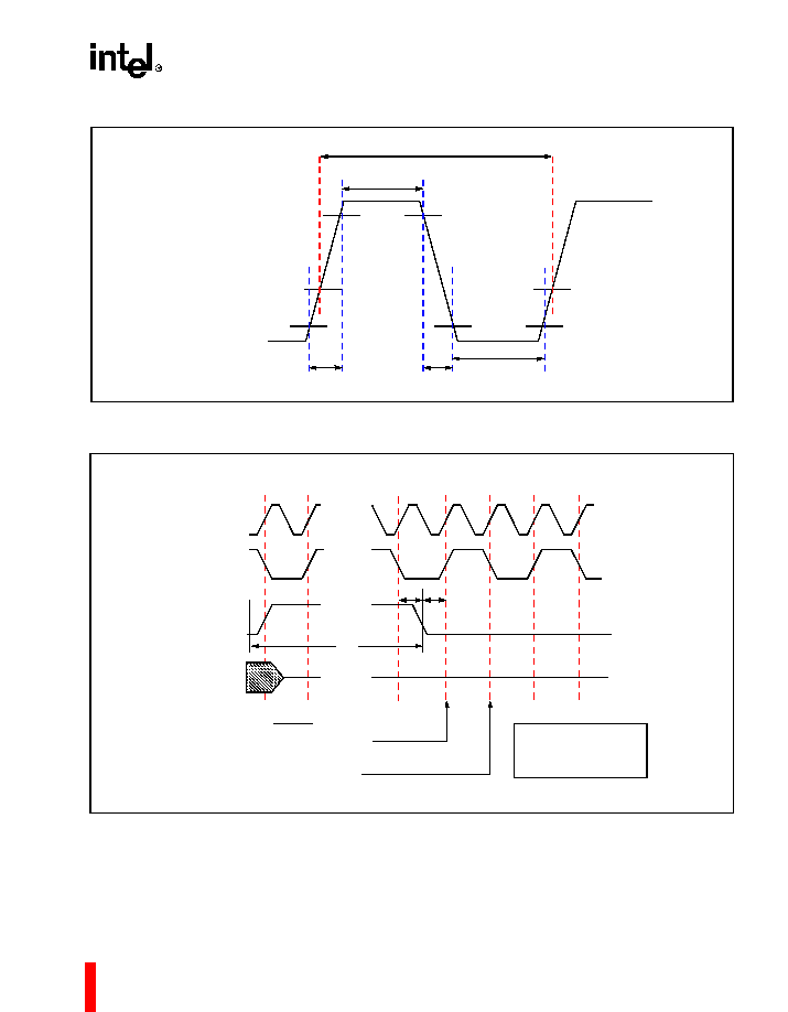
AC Specifications
This section describes the AC specifications for the
80960MC pins. All input and output timings are spec-
ified relative to the 1.5 V level of the rising edge of
CLK2. For output timings the specifications refer to
the time it takes the signal to reach 1.5 V.
For input timings the specifications refer to the time
at which the signal reaches (for input setup) or
leaves (for hold time) the TTL levels of LOW (0.8 V)
or HIGH (2.0 V). All AC testing should be done with
input voltages of 0.4 V and 2.4 V, except for the
clock (CLK2), which should be tested with input
voltages of 0.45 V and 0.55 V
CC
.
Figure 13. Drive Levels and Timing Relationships for 80960MC Signals
A
B
C
D
A
B
C
1.5V
1.5V
1.5V
1.5V
0.8V
T
6
1.5V
1.5V
T
7
1.5V
1.5V
VALID OUTPUT
T
6
T
8
T
8
T
13
T
14
1.5V
1.5V
VALID OUTPUT
T
9
2.0V
2.0V
2.0V
2.0V
0.8V
0.8V
0.8V
0.8V
EDGE
CLK2
OUTPUTS:
LAD 31:0
ADS
W/R, DEN
BE3:0
HLDA/HOLDR
CACHE
LOCK, INTA
ALE
DT/R
INPUTS:
LAD31:0
BADAC
IAC/INT0, INT1
INT2/INTR, INT3
HOLD, HLDAR
LOCK
READY
T
9
VALID INPUT
T
10
T
11
T
12
T
11

80960MC
19
Figure 14. Timing Relationship of L-Bus Signals
Figure 15. System and Processor Clock Relationship
A4484-01
READY#
DEN#
DT/R
W/R#
BE(0:3)#
ADS#
ALE#
LAD
(31-0)
CLK
CLK2
T11
T12
T11
T12
T11
T12
T6
T6
T6
T6
T9
T13
T14
T9
T13
14
T
T7
T6
Address
Data
T13
T8 T14
T9
T10
T11
T6
T13
Address
Data
T9
T6
T9
T8
T7
T
T
T
a
d
r
T
T
T
a
d
r
T2
T3
Td
T1
T9
CLK
CLK2
T
Ta
Td
r
Bus
State
Bus
State
Bus
State
80960MC
20
1. Clock rise and fall times are not tested.
2. A float condition occurs when the maximum output current becomes less than I
LO
. Float delay is not tested; however, it
should not be longer than the valid delay.
3. LAD31:0,
BADAC, HOLD, LOCK and READY are synchronous inputs. IAC/INT
0
, INT
1
, INT
2
/INT
R
and INT
3
may be syn-
chronous or asynchronous.
Table 7. 80960MC AC Characteristics (25 MHz)
Symbol
Parameter
Min
Max
Units
Notes
Input Clock
T
1
Processor Clock Period (CLK2)
20
125
ns
V
IN
= 1.5V
T
2
Processor Clock Low Time (CLK2)
5
ns
V
IL
= 10% Point = 1.2V
T
3
Processor Clock High Time (CLK2)
5
ns
V
IH
= 90% Point = 0.1V + 0.5 V
CC
T
4
Processor Clock Fall Time (CLK2)
10
ns
V
IN
= 90% Point to 10% Point (1)
T
5
Processor Clock Rise Time (CLK2)
10
ns
V
IN
= 10% Point to 90% Point (1)
Synchronous Outputs
T
6
Output Valid Delay
2
18
ns
T
6H
HLDA Output Valid Delay
4
23
ns
T
7
ALE Width
12
ns
T
8
ALE Output Valid Delay
2
18
ns
T
9
Output Float Delay
2
18
ns
(2)
T
9H
HLDA Output Float Delay
4
20
ns
(2)
Synchronous Inputs
T
10
Input Setup 1
3
ns
(3)
T
11
Input Hold
5
ns
(3)
T
11H
HOLD Input Hold
4
ns
T
12
Input Setup 2
7
ns
T
13
Setup to ALE Inactive
8
ns
T
14
Hold after ALE Inactive
8
ns
T
15
Reset Hold
3
ns
T
16
Reset Setup
5
ns
T
17
Reset Width
820
ns
41 CLK2 Periods Minimum
NOTES:
80960MC
21
Figure 16. Processor Clock Pulse (CLK2)
Figure 17. RESET Signal Timing
HIGH LEVEL (MIN) 0.55V
CC
LOW LEVEL (MAX) 0.8V
T
1
T
3
T
5
T
4
T
2
90%
10%
1.5 V
...
...
...
...
CLK2
CLK
RESET
OUTPUTS
FIRST
A
B
C
D
A
INIT PARAMETERS (BADAC,
INT
0
/IAC) MUST BE SET UP 8 CLOCKS
PRIOR TO THIS CLK2 EDGE
INIT PARAMETERS MUST BE HELD
BEYOND THIS CLK2 EDGE
T
15
= RESET HOLD
T
16
= RESET SETUP
T
17
= RESET WIDTH
T
15
T
16
T
17

80960MC
22
Figure 18. HOLD Timing
A4490-01
HOLDR
HOLDAR
D
Secondary
D
HOLD
HLDA
Primary
Delay of 5 ns Minimum
is Required
Th
Th
Th
Th
CLK2
CLK
HOLDR
HOLD
HLDA
HLDAR
T9h
T11h
T9h
T11h
T12
T6h
T12
T6h
2.9
Design Considerations
Input hold times can be disregarded by the designer
whenever the input is removed because a subse-
quent output from the processor is deasserted (e.g.,
DEN becomes deasserted).
In other words, whenever the processor generates
an output that indicates a transition into a subse-
quent state, the processor must have sampled any
inputs for the previous state.
Similarly, whenever the processor generates an
output that indicates a transition into a subsequent
state, any outputs that are specified to be three
stated in this new state are guaranteed to be three
stated.
3.0
MECHANICAL DATA
3.1
Packaging
The 80960MC is available in one package type: a
132-lead ceramic pin-grid array (PGA). Pins are
arranged 0.100 inch (2.54 mm) center-to-center, in a
14 by 14 matrix, three rows around (see
Figure 20
).
Dimensions for the PGA package type is given in the
Intel
Packaging
handbook (Order #240800).
3.1.1
Pin Assignment
Figure 21
shows the view from the PGA bottom (pins
facing up).
Table 8
and
Table 9
list the function of
each PGA pin.

80960MC
23
Figure 19. 132-Lead Pin-Grid Array (PGA) Package
1
2
3
A
B
C
D
E
F G
H
J
K
L M
N
P
4
5
6
7
8
9
10
11
12
13
14
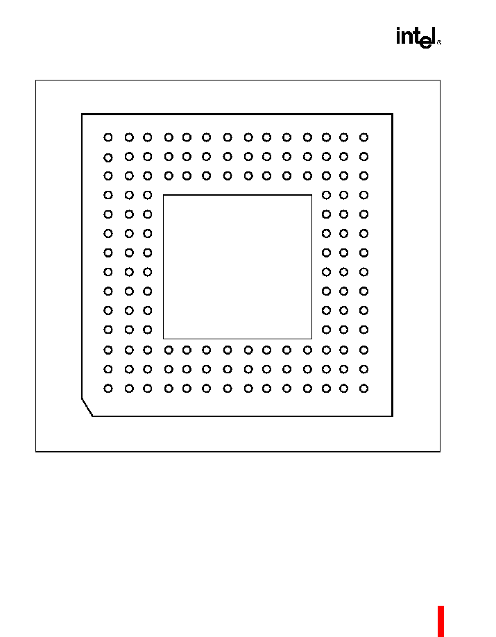
80960MC
24
Figure 20. 80960MC PGA Pinout--View from Bottom (Pins Facing Up)
V
CC
V
SS
N.C.
N.C.
N.C.
N.C.
N.C.
N.C.
N.C.
N.C.
N.C.
N.C.
N.C.
V
CC
N.C.
N.C.
N.C.
N.C.
N.C.
N.C.
N.C.
N.C.
N.C.
N.C.
N.C.
N.C.
N.C.
V
SS
N.C.
N.C.
N.C.
V
CC
V
SS
N.C.
N.C.
N.C.
N.C.
V
CC
V
SS
V
CC
N.C.
V
SS
V
CC
N.C.
DEN
V
SS
FAIL
BE
3
V
SS
BE
2
DT/R
LOCK
BE
0
W/R
BE
1
READY
LAD
30
CACHE
LAD
31
LAD
29
LAD
27
LAD
26
LAD
28
HLDA
ADS
ALE
N.C.
N.C.
N.C.
N.C.
N.C.
N.C.
N.C.
N.C.
N.C.
N.C.
N.C.
N.C.
N.C.
N.C.
N.C.
N.C.
N.C.
N.C.
N.C.
N.C.
V
SS
V
CC
V
SS
V
CC
V
SS
V
SS
V
SS
V
SS
V
CC
V
CC
V
CC
V
CC
INT
2
INT
0
INT
1
INT
3
LAD
3
LAD
8
LAD
20
LAD
13
BADAC
HOLD LAD
25
RESET
LAD
0
LAD
1
LAD
4
LAD
5
LAD
7
LAD
9
LAD
11
LAD
14
LAD
16
LAD
17
LAD
19
LAD
2
LAD
6
LAD
10
LAD
12
LAD
15
LAD
18
LAD
21
LAD
22
LAD
24
LAD
23
CLK2
P
N
M
L
K
J
H
G
F
E
D
C
B
A
P
N
M
L
K
J
H
G
F
E
D
C
B
A
14
13
12
11
10
9
8
7
6
5
4
3
2
1
14
13
12
11
10
9
8
7
6
5
4
3
2
1

80960MC
25
Figure 21. 80960MC PGA Pinout--View from Top (Pins Facing Down)
V
CC
V
SS
N.C.
N.C.
N.C.
N.C.
N.C.
N.C.
N.C.
N.C.
N.C.
N.C.
N.C.
V
CC
N.C.
N.C.
N.C.
N.C.
N.C.
N.C.
N.C.
N.C.
N.C.
N.C.
N.C.
N.C.
N.C.
V
SS
N.C.
N.C.
N.C.
V
CC
V
SS
N.C.
N.C.
N.C.
N.C.
V
CC
V
SS
V
CC
N.C.
V
SS
V
CC
N.C.
DEN
V
SS
FAIL
BE
3
V
SS
BE
2
DT/R
LOCK
BE
0
W/R
BE
1
READY LAD
30
CACHE LAD
31
LAD
29
LAD
27
LAD
26
LAD
28
HLDA ADS
ALE
N.C.
N.C.
N.C.
N.C.
N.C.
N.C.
N.C.
N.C.
N.C.
N.C.
N.C.
N.C.
N.C.
N.C.
N.C.
N.C.
N.C.
N.C.
N.C.
N.C.
V
SS
V
CC
V
SS
V
CC
V
SS
V
SS
V
SS
V
SS
V
CC
V
CC
V
CC
V
CC
INT
2
INT
0
INT
1
INT
3
LAD
3
LAD
8
LAD
20
LAD
13
BADAC
HOLD
LAD
25
RESET LAD
0
LAD
1
LAD
4
LAD
5
LAD
7
LAD
9
LAD
11
LAD
14
LAD
16
LAD
17
LAD
19
LAD
2
LAD
6
LAD
10
LAD
12
LAD
15
LAD
18
LAD
21
LAD
22
LAD
24
LAD
23
CLK2
P
N
M
L
K
J
H
G
F
E
D
C
B
A
P
N
M
L
K
J
H
G
F
E
D
C
B
A
14
13
12
11
10
9
8
7
6
5
4
3
2
1
14
13
12
11
10
9
8
7
6
5
4
3
2
1
A
80960
MC
-2
5
X
XXXXX
XX
X
XXXXX
X
XXXXX
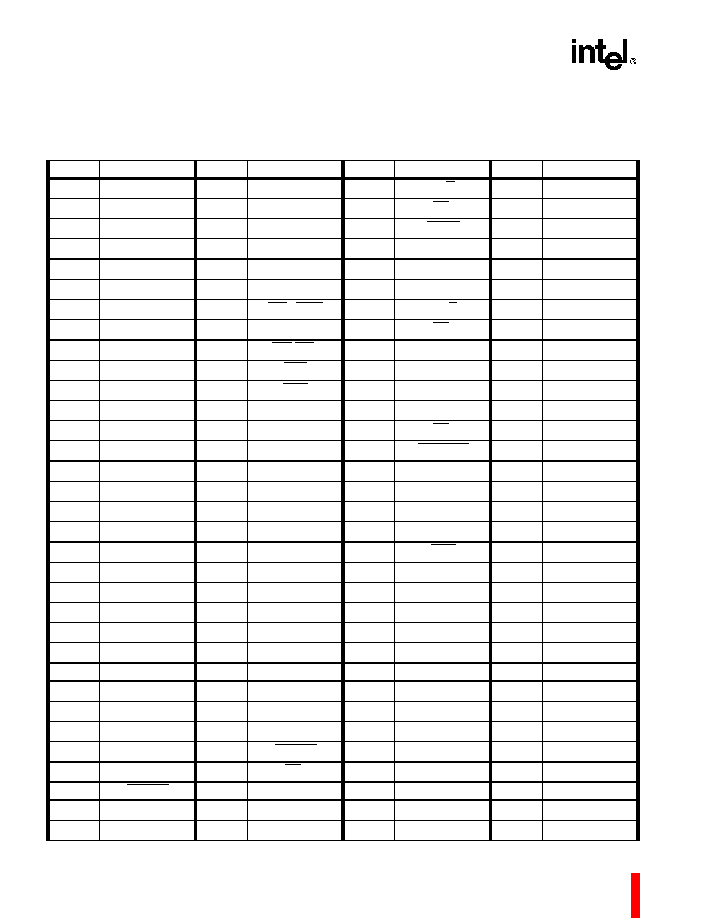
80960MC
26
3.2
Pinout
NOTES:
Do not connect any external logic to any pins marked N.C.
Table 8. 80960MC PGA Pinout -- In Pin Order
Pin
Signal
Pin
Signal
Pin
Signal
Pin
Signal
A1
V
CC
C6
LAD
20
H1
W/R
M10
V
SS
A2
V
SS
C7
LAD
13
H2
BE
0
M11
V
CC
A3
LAD
19
C8
LAD
8
H3
LOCK
M12
N.C.
A4
LAD
17
C9
LAD
3
H12
N.C.
M13
N.C.
A5
LAD
16
C10
V
CC
H13
N.C.
M14
N.C.
A6
LAD
14
C11
V
SS
H14
N.C.
N1
V
SS
A7
LAD
11
C12
INT
3
/INTA
J1
DT/R
N2
N.C.
A8
LAD
9
C13
INT
1
J2
BE
2
N3
N.C.
A9
LAD
7
C14
IAC/INT
0
J3
V
SS
N4
N.C.
A10
LAD
5
D1
ALE
J12
N.C.
N5
N.C.
A11
LAD
4
D2
ADS
J13
N.C.
N6
N.C.
A12
LAD
1
D3
HLDA/HOLDR
J14
N.C.
N7
N.C.
A13
INT
2
/INTR
D12
V
CC
K1
BE
3
N8
N.C.
A14
V
CC
D13
N.C.
K2
FAILURE
N9
N.C.
B1
LAD
23
D14
N.C.
K3
V
SS
N10
N.C.
B2
LAD
24
E1
LAD
28
K12
V
CC
N11
N.C.
B3
LAD
22
E2
LAD
26
K13
N.C.
N12
N.C.
B4
LAD
21
E3
LAD
27
K14
N.C.
N13
N.C.
B5
LAD
18
E12
N.C.
L1
DEN
N14
N.C.
B6
LAD
15
E13
V
SS
L2
N.C.
P1
V
CC
B7
LAD
12
E14
N.C.
L3
V
CC
P2
N.C.
B8
LAD
10
F1
LAD
29
L12
V
SS
P3
N.C.
B9
LAD
6
F2
LAD
31
L13
N.C.
P4
N.C.
B10
LAD
2
F3
CACHE/TAG
L14
N.C.
P5
N.C.
B11
CLK2
F12
N.C.
M1
N.C.
P6
N.C.
B12
LAD
0
F13
N.C.
M2
V
CC
P7
N.C.
B13
RESET
F14
N.C.
M3
V
SS
P8
N.C.
B14
V
SS
G1
LAD
30
M4
V
SS
P9
N.C.
C1
HOLD/HLDAR
G2
READY
M5
V
CC
P10
N.C.
C2
LAD
25
G3
BE
1
M6
N.C.
P11
N.C.
C3
BADAC
G12
N.C.
M7
N.C.
P12
N.C.
C4
V
CC
G13
N.C.
M8
N.C.
P13
V
SS
C5
V
SS
G14
N.C.
M9
N.C.
P14
V
CC

80960MC
27
NOTE:
Do not connect external logic to any pins marked N.C.
Table 9. 80960MC PGA Pinout -- In Signal Order
Signal
Pin
Signal
Pin
Signal
Pin
Signal
Pin
ADS
D2
LAD
15
B6
N.C.
J14
N.C.
P9
ALE
D1
LAD
16
A5
N.C.
K13
N.C.
P10
BADAC
C3
LAD
17
A4
N.C.
K14
N.C.
P11
BE
0
H2
LAD
18
B5
N.C.
L13
N.C.
P12
BE
1
G3
LAD
19
A3
N.C.
L14
N.C.
L2
BE
2
J2
LAD
20
C6
N.C.
M1
READY
G2
BE
3
K1
LAD
21
B4
N.C.
M6
RESET
B13
CACHE
F3
LAD
22
B3
N.C.
M7
V
CC
A1
CLK2
B11
LAD
23
B1
N.C.
M8
V
CC
A14
DEN
L1
LAD
24
B2
N.C.
M9
V
CC
C4
DT/R
J1
LAD
25
C2
N.C.
M12
V
CC
C10
FAILURE
K2
LAD
26
E2
N.C.
M13
V
CC
D12
HLDA/HOLDR
D3
LAD
27
E3
N.C.
M14
V
CC
K12
HOLD/HLDAR
C1
LAD
28
E1
N.C.
N2
V
CC
L3
IAC/INT
0
C14
LAD
29
F1
N.C.
N3
V
CC
M2
INT
1
C13
LAD
30
G1
N.C.
N4
V
CC
M5
INT
2
/INTR
A13
LAD
31
F2
N.C.
N5
V
CC
M11
INT
3
/INTA
C12
LOCK
H3
N.C.
N6
V
CC
P1
LAD
0
B12
N.C.
D13
N.C.
N7
V
CC
P14
LAD
1
A12
N.C.
D14
N.C.
N8
V
SS
A2
LAD
2
B10
N.C.
E12
N.C.
N9
V
SS
B14
LAD
3
C9
N.C.
E14
N.C.
N10
V
SS
C5
LAD
4
A11
N.C.
F12
N.C.
N11
V
SS
C11
LAD
5
A10
N.C.
F13
N.C.
N12
V
SS
E11
LAD
6
B9
N.C.
F14
N.C.
N13
V
SS
J3
LAD
7
A9
N.C.
G12
N.C.
N14
V
SS
K3
LAD
8
C8
N.C.
G13
N.C.
P2
V
SS
L12
LAD
9
A8
N.C.
G14
N.C.
P3
V
SS
M3
LAD
10
B8
N.C.
H12
N.C.
P4
V
SS
M4
LAD
11
A7
N.C.
H13
N.C.
P5
V
SS
M10
LAD
12
B7
N.C.
H14
N.C.
P6
V
SS
N1
LAD
13
C7
N.C.
J12
N.C.
P7
V
SS
P13
LAD
14
A6
N.C.
J13
N.C.
P8
W/R
H1
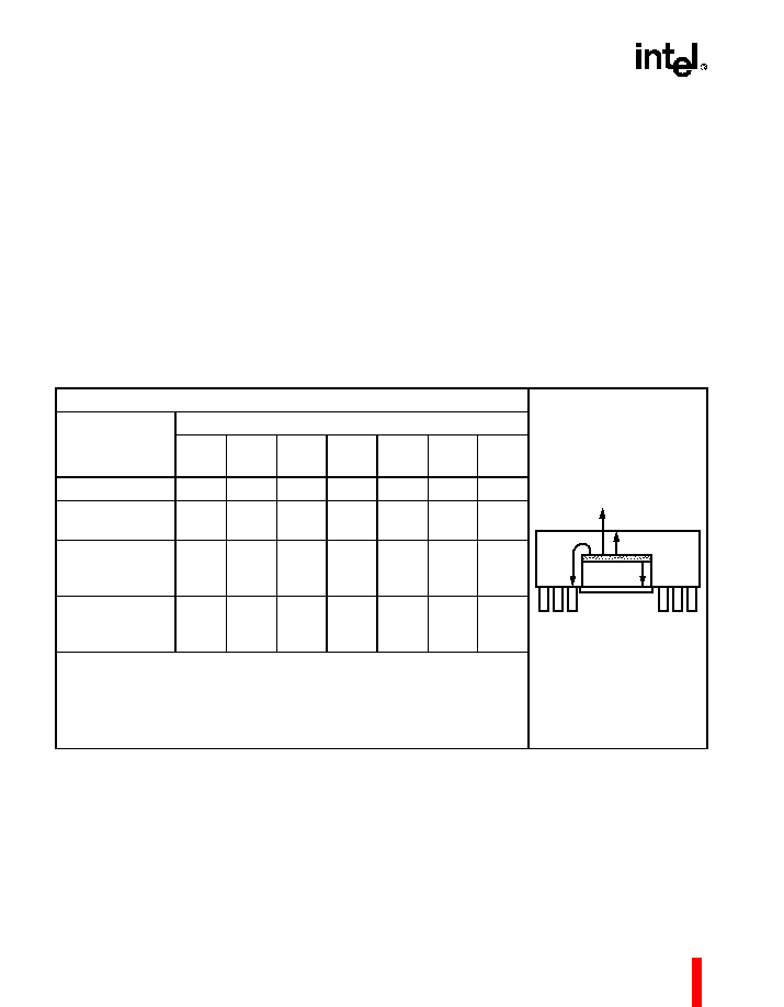
28
80960MC
3.3
Package Thermal Specification
The 80960MC is specified for operation when case
temperature is within the range 0∞C to 85∞C (PGA).
Measure case temperature at the top center of the
package. Ambient temperature can be calculated
from:
∑
T
J
= T
C
+ P*
jc
∑
T
A
= T
J
+ P*
ja
∑
T
C
= T
A
+ P*
[
ja
-
jc
]
Values for
ja
and
jc
for various airflows are given in
Table 10
for the PGA package. The PGA's
ja
can
be reduced by adding a heatsink.
Maximum allowable ambient temperature (T
A
)
permitted without exceeding T
C
is shown by the
graphs in
Figure 23
,
Figure 24
and
Figure 25
. The
curves assume the maximum permitted supply
current (I
CC
) at each speed, V
CC
of +5.0 V and a
T
CASE
of +85∞ C (PGA).
Table 10. 80960MC PGA Package Thermal Characteristics
Thermal Resistance -- ∞C/Watt
Parameter
Airflow -- ft./min (m/sec)
0
(0)
50
(0.25)
100
(0.50)
200
(1.01)
400
(2.03)
600
(3.04)
800
(4.06)
Junction-to-Case
2
2
2
2
2
2
2
Case-to-Ambient
(No Heatsink)
19
18
17
15
12
10
9
Case-to-Ambient
(Omnidirectional
Heatsink)
16
15
14
12
9
7
6
Case-to-Ambient
(Unidirectional
Heatsink)
15
14
13
11
8
6
5
NOTES:
1. This table applies to 80960MC PGA plugged into socket or soldered directly to board.
2.
JA
=
JC
+
CA
3.
J-CAP
= 4∞C/W (approx.)
J-PIN
= 4∞C/W (inner pins) (approx.)
J-PIN
= 8∞C/W (outer pins) (approx.)
JC
JA
J-PIN
J-CAP
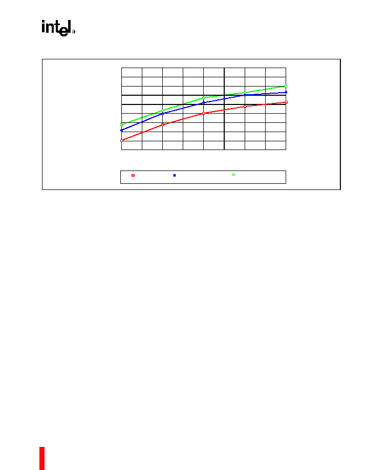
80960MC
29
Figure 22. 25 MHz Maximum Allowable Ambient Temperature
AIRFLOW (ft/min)
T
E
M
P
E
RAT
U
R
E
(
o
C)
80
75
70
65
60
55
50
45
40
0
100
200
300
400
500
600
700
800
PGA with no
heatsink
PGA with omni-
directional heatsink
PGA with uni-
directional heatsink
85

80960MC
30
4.0
WAVEFORMS
The following figures present waveforms for various transactions on the 80960MC'S local bus:
∑
Figure 23, Non-Burst Read and Write Transactions Without Wait States (pg. 30)
∑
Figure 24, Burst Read and Write Transaction Without Wait States (pg. 31)
∑
Figure 25, Burst Write Transaction with 2, 1, 1, 1 Wait States (pg. 32)
∑
Figure 26, Accesses Generated by Quad Word Read Bus Request, Misaligned Two Bytes from Quad Word
Boundary (1, 0, 0, 0 Wait States) (pg. 33)
∑
Figure 27, Interrupt Acknowledge Transaction (pg. 34)
∑
Figure 28, Bus Exchange Transaction (PBM = Primary Bus Master, SBM = Secondary Bus Master) (pg. 35)
Figure 23. Non-Burst Read and Write Transactions Without Wait States
T
a
T
d
T
r
T
a
T
d
T
r
CLK2
CLK
LAD31:0
ALE
ADS
BE3:0
W/R
DT/R
DEN
READY
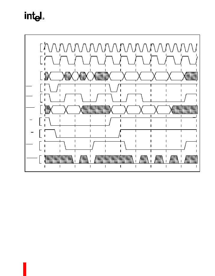
80960MC
31
Figure 24. Burst Read and Write Transaction Without Wait States
T
a
T
d
T
d
T
r
T
a
T
d
T
d
T
d
T
d
T
r
CLK2
CLK
LAD31:0
ALE
ADS
BE3:0
W/R
DT/R
DEN
READY
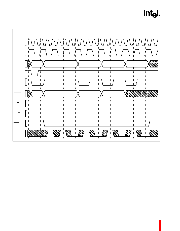
80960MC
32
Figure 25. Burst Write Transaction with 2, 1, 1, 1 Wait States
T
a
T
w
T
w
T
d
T
w
T
d
T
w
T
d
T
w
T
d
T
r
CLK2
CLK
LAD31:0
ALE
ADS
BE3:0
W/R
DT/R
DEN
READY

80960MC
33
Figure 26. Accesses Generated by Quad Word Read Bus Request, Misaligned Two Bytes from Quad
Word Boundary (1, 0, 0, 0 Wait States)
T
a
T
w
T
d
T
d
T
d
T
d
T
r
T
a
T
w
T
d
T
r
CLK2
CLK
LAD31:0
ALE
ADS
BE3:2
W/R
DT/R
DEN
READY
BE1:0

80960MC
34
Figure 27. Interrupt Acknowledge Transaction
CLK2
T
X
T
X
T
a
T
d
T
r
T
r
T
I
T
I
T
I
T
I
T
I
T
a
T
w
T
d
INTR
LAD31:0
ALE
ADS
INTA
DT/R
DEN
LOCK
READY
NOTE:
INTR can go low no sooner than the input hold time following the beginning of interrupt acknowledgment cycle 1.
For a second interrupt to be acknowledged, INTR must be low for at least three cycles before it can be reasserted.
INTERRUPT
ACKNOWLEDGEMENT
CYCLE 1
IDLE
(5 BUS STATES)
INTERRUPT
ACKNOWLEDGEMENT
CYCLE 2
PREVIOUS
CYCLE
ADDR
VECTOR
ADDR
CLK

80960MC
35
Figure 28. Bus Exchange Transaction (PBM = Primary Bus Master, SBM = Secondary Bus Master)
5.0
REVISION HISTORY
No revision history was maintained in earlier revisions of this data sheet. All errata that has been identified to
date is incorporated into this revision. The sections significantly changed since the previous revision are:
Section
Last
Rev.
Description
This is the initial commercial data sheet for the A80960MC.
A4492-01
LAD
31
CLK
T
T
T
a
d
h
T
T
T
a
d
r
Addr
Data
Addr
Data
Addr
Data
Data
Data
Data
Addr
Th
Th
Th
Th
Th
Th
Th
Td
Th
Thr
Thr
Thr
Ta
Td
Tr
Thr
Thr
Thr
Thr
Ta
Td
Td
Ti
Ti
Th
Th
Th
Th
W/R#
LAD
0
_
PBM ALE#
SBM ALE#
READY#
SBM
HOLDR
PBM
HOLD
PBM
HLDA
SBM
HLDAR
PBM BUS
STATE
SBM BUS
STATE