Other brands and names are the property of their respective owners
Information in this document is provided in connection with Intel products Intel assumes no liability whatsoever including infringement of any patent or
copyright for sale and use of Intel products except as provided in Intel's Terms and Conditions of Sale for such products Intel retains the right to make
changes to these specifications at any time without notice Microcomputer Products may have minor variations to this specification known as errata
June, 2002
COPYRIGHT
© INTEL CORPORATION, 2002
Order Number: 272433-005
80C186EB 80C188EB AND 80L186EB 80L188EB
16-BIT HIGH-INTEGRATION EMBEDDED PROCESSORS
X
Full Static Operation
X
True CMOS Inputs and Outputs
Y
Integrated Feature Set
Low-Power Static CPU Core
Two Independent UARTs each with
an Integral Baud Rate Generator
Two 8-Bit Multiplexed I O Ports
Programmable Interrupt Controller
Three Programmable 16-Bit
Timer Counters
Clock Generator
Ten Programmable Chip Selects with
Integral Wait-State Generator
Memory Refresh Control Unit
System Level Testing Support (ONCE
Mode)
Y
Direct Addressing Capability to 1 Mbyte
Memory and 64 Kbyte I O
Y
Speed Versions Available (5V)
25 MHz (80C186EB25 80C188EB25)
20 MHz (80C186EB20 80C188EB20)
13 MHz (80C186EB13 80C188EB13)
Y
Available in Extended Temperature
Range (
b
40 C to
a
85 C)
Y
Speed Versions Available (3V)
16 MHz (80L186EB16 80L188EB16)
13 MHz (80L186EB13 80L188EB13)
Y
Low-Power Operating Modes
Idle Mode Freezes CPU Clocks but
keeps Peripherals Active
Powerdown Mode Freezes All
Internal Clocks
Y
Supports 80C187 Numeric Coprocessor
Interface (80C186EB PLCC Only)
Y
Available In
80-Pin Quad Flat Pack (QFP)
84-Pin Plastic Leaded Chip Carrier
(PLCC)
80-Pin Shrink Quad Flat Pack (SQFP)
The 80C186EB is a second generation CHMOS High-Integration microprocessor It has features that are new
to the 80C186 family and include a STATIC CPU core an enhanced Chip Select decode unit two independent
Serial Channels I O ports and the capability of Idle or Powerdown low power modes
272433 ≠ 1

80C186EB 80C188EB and 80L186EB 80L188EB
16-Bit High-Integration Embedded Processors
CONTENTS
PAGE
INTRODUCTION
4
CORE ARCHITECTURE
4
Bus Interface Unit
4
Clock Generator
4
80C186EC PERIPHERAL
ARCHITECTURE
5
Interrupt Control Unit
5
Timer Counter Unit
5
Serial Communications Unit
7
Chip-Select Unit
7
I O Port Unit
7
Refresh Control Unit
7
Power Management Unit
7
80C187 Interface (80C186EB Only)
7
ONCE Test Mode
7
PACKAGE INFORMATION
8
Prefix Identification
8
Pin Descriptions
8
80C186EB PINOUT
14
PACKAGE THERMAL
SPECIFICATIONS
22
ELECTRICAL SPECIFICATIONS
23
Absolute Maximum Ratings
23
CONTENTS
PAGE
Recommended Connections
23
DC SPECIFICATIONS
24
I
CC
versus Frequency and Voltage
27
PDTMR Pin Delay Calculation
27
AC SPECIFICATIONS
28
AC Characteristics
80C186EB25
28
AC Characteristics
80C186EB20 13
30
AC Characteristics
80L186EB16
32
Relative Timings
36
Serial Port Mode 0 Timings
37
AC TEST CONDITIONS
38
AC TIMING WAVEFORMS
38
DERATING CURVES
41
RESET
42
BUS CYCLE WAVEFORMS
45
EXECUTION TIMINGS
52
INSTRUCTION SET SUMMARY
53
ERRATA
59
REVISION HISTORY
59
2

80C186EB 80C188EB 80L186EB 80L188EB
272433 ≠ 2
NOTE
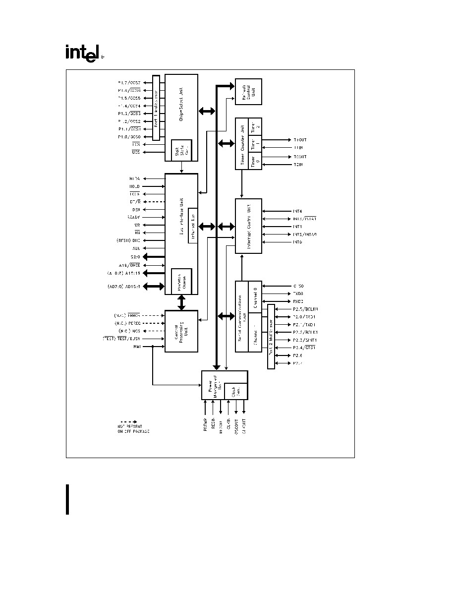
Pin names in parentheses apply to the 80C188EB 80L188EB
Figure 1 80C186EB 80C188EB Block Diagram
3

80C186EB 80C188EB 80L186EB 80L188EB
INTRODUCTION
Unless specifically noted
all references to the
80C186EB apply to the 80C188EB 80L186EB and
80L188EB References to pins that differ between
the 80C186EB 80L186EB and the 80C188EB
80L188EB are given in parentheses The ``L'' in the
part number denotes low voltage operation Physi-
cally and functionally the ``C'' and ``L'' devices are
identical
The 80C186EB is the first product in a new genera-
tion of low-power high-integration microprocessors
It enhances the existing 186 family by offering new
features and new operating modes The 80C186EB
is object code compatible with the 80C186XL
80C188XL microprocessors
The 80L186EB is the 3V version of the 80C186EB
The 80L186EB is functionally identical to the
80C186EB
embedded
processor
Current
80C186EB users can easily upgrade their designs to
use the 80L186EB and benefit from the reduced
power consumption inherent in 3V operation
The feature set of the 80C186EB meets the needs
of low power space critical applications Low-Power
applications benefit from the static design of the
CPU core and the integrated peripherals as well as
low voltage operation Minimum current consump-
tion is achieved by providing a Powerdown mode
that halts operation of the device and freezes the
clock circuits Peripheral design enhancements en-
sure that non-initialized peripherals consume little
current
Space critical applications benefit from the inte-
gration of commonly used system peripherals Two
serial channels are provided for services such as
diagnostics inter-processor communication modem
interface terminal display interface and many oth-
ers A flexible chip select unit simplifies memory and
peripheral interfacing The interrupt unit provides
sources for up to 129 external interrupts and will pri-
oritize these interrupts with those generated from
the on-chip peripherals Three general purpose tim-
er counters and sixteen multiplexed I O port pins
round out the feature set of the 80C186EB
Figure 1 shows a block diagram of the 80C186EB
80C188EB The Execution Unit (EU) is an enhanced
8086 CPU core that includes dedicated hardware to
speed up effective address calculations enhance
execution speed for multiple-bit shift and rotate in-
structions and for multiply and divide instructions
string move instructions that operate at full bus
bandwidth ten new instruction and fully static oper-
ation The Bus Interface Unit (BIU) is the same as
that found on the original 186 family products ex-
cept the queue status mode has been deleted and
buffer interface control has been changed to ease
system design timings An independent internal bus
is used to allow communication between the BIU
and internal peripherals
CORE ARCHITECTURE
Bus Interface Unit
The 80C186EB core incorporates a bus controller
that generates local bus control signals In addition
it employs a HOLD HLDA protocol to share the local
bus with other bus masters
The bus controller is responsible for generating 20
bits of address read and write strobes bus cycle
status information and data (for write operations) in-
formation It is also responsible for reading data off
the local bus during a read operation A READY in-
put pin is provided to extend a bus cycle beyond the
minimum four states (clocks)
The local bus controller also generates two control
signals (DEN and DT R) when interfacing to exter-
nal transceiver chips (Both DEN and DT R are
available on the PLCC devices only DEN is avail-
able on the QFP and SQFP devices ) This capability
allows the addition of transceivers for simple buffer-
ing of the multiplexed address data bus
Clock Generator
The processor provides an on-chip clock generator
for both internal and external clock generation The
clock generator features a crystal oscillator a divide-
by-two counter
and two low-power operating
modes
The oscillator circuit is designed to be used with ei-
ther a parallel resonant fundamental or third-over-
tone mode crystal network Alternatively the oscilla-
tor circuit may be driven from an external clock
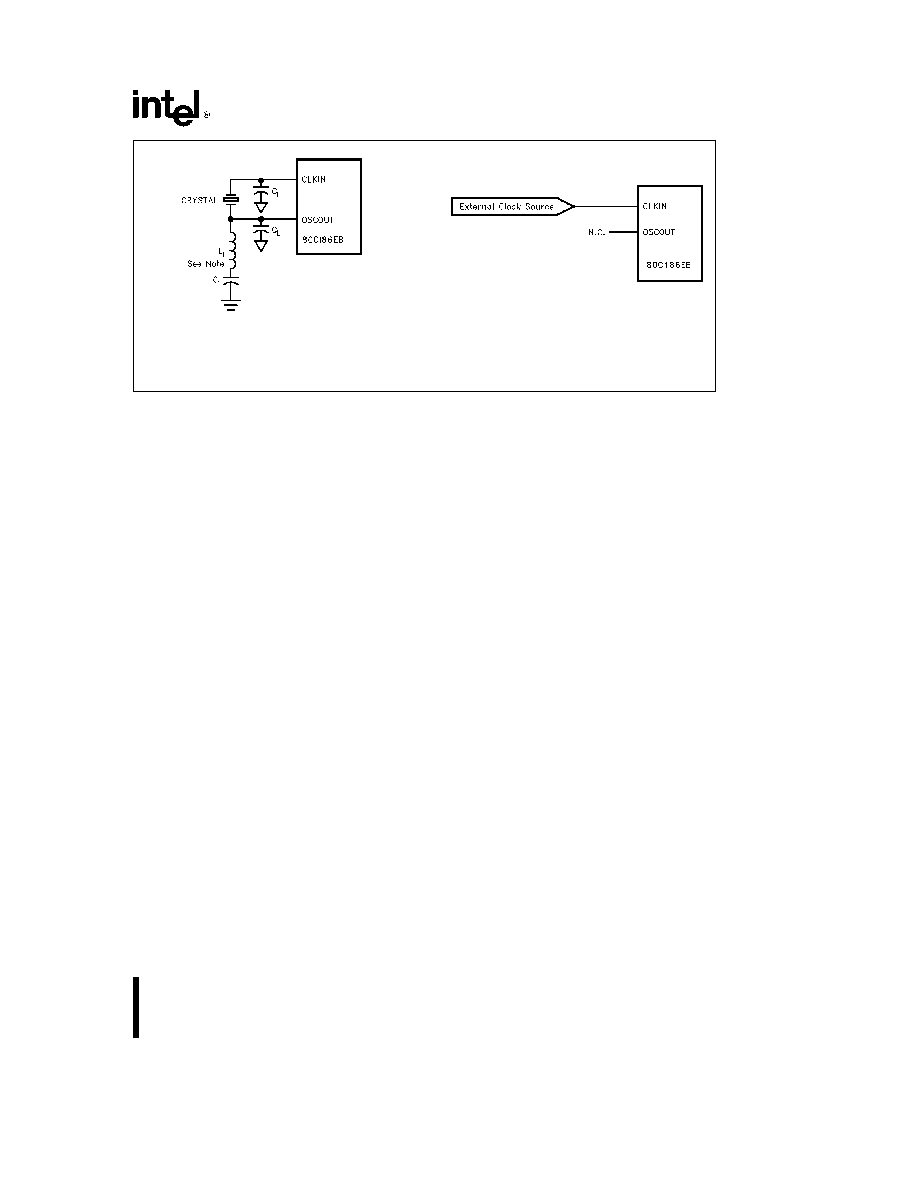
source Figure 2 shows the various operating modes
of the oscillator circuit
The crystal or clock frequency chosen must be twice
the required processor operating frequency due to
the internal divide-by-two counter This counter is
used to drive all internal phase clocks and the exter-
nal CLKOUT signal CLKOUT is a 50% duty cycle
processor clock and can be used to drive other sys-
tem components All AC timings are referenced to
CLKOUT
4

80C186EB 80C188EB 80L186EB 80L188EB
272433 ≠ 3
(A) Crystal Connection
NOTE
The L
1
C
1
network is only required when using a third-
overtone crystal
272433 ≠ 4
(B) Clock Connection
Figure 2 Clock Configurations
The following parameters are recommended when
choosing a crystal
Temperature Range
Application Specific
ESR (Equivalent Series Resistance)
40X max
C0 (Shunt Capacitance of Crystal)
7 0 pF max
C
L
(Load Capacitance)
20 pF
g
2 pF
Drive Level
1 mW max
80C186EB PERIPHERAL
ARCHITECTURE
The 80C186EB has integrated several common sys-
tem peripherals with a CPU core to create a com-
pact yet powerful system The integrated peripher-
als are designed to be flexible and provide logical
interconnections between supporting units (e g the
interrupt control unit supports interrupt requests
from the timer counters or serial channels)
The list of integrated peripherals includes
7-Input Interrupt Control Unit
3-Channel Timer Counter Unit
2-Channel Serial Communications Unit
10-Output Chip-Select Unit
I O Port Unit
Refresh Control Unit
Power Management Unit
The registers associated with each integrated peri-
heral are contained within a 128 x 16 register file
called the Peripheral Control Block (PCB) The PCB
can be located in either memory or I O space on
any 256 Byte address boundary
Figure 3 provides a list of the registers associated
with the PCB The Register Bit Summary at the end
of this specification individually lists all of the regis-
ters and identifies each of their programming attri-
butes
Interrupt Control Unit
The 80C186EB can receive interrupts from a num-
ber of sources both internal and external The inter-
rupt control unit serves to merge these requests on
a priority basis for individual service by the CPU
Each interrupt source can be independently masked
by the Interrupt Control Unit (ICU) or all interrupts
can be globally masked by the CPU
Internal interrupt sources include the Timers and Se-
rial channel 0 External interrupt sources come from
the five input pins INT4 0 The NMI interrupt pin is
not controlled by the ICU and is passed directly to
the CPU Although the Timer and Serial channel
each have only one request input to the ICU sepa-
rate vector types are generated to service individual
interrupts within the Timer and Serial channel units
Timer Counter Unit
The 80C186EB Timer Counter Unit (TCU) provides
three 16-bit programmable timers Two of these are
highly flexible and are connected to external pins for
control or clocking A third timer is not connected to
any external pins and can only be clocked internally
However it can be used to clock the other two timer
channels The TCU can be used to count external
events time external events generate non-repeti-
tive waveforms generate timed interrupts etc
5
