Other brands and names are the property of their respective owners
Information in this document is provided in connection with Intel products Intel assumes no liability whatsoever including infringement of any patent or
copyright for sale and use of Intel products except as provided in Intel's Terms and Conditions of Sale for such products Intel retains the right to make
changes to these specifications at any time without notice Microcomputer Products may have minor variations to this specification known as errata
May 1996
COPYRIGHT
INTEL CORPORATION 1996
Order Number 272434-004
80C186EC 80C188EC AND 80L186EC 80L188EC
16-BIT HIGH-INTEGRATION EMBEDDED PROCESSORS
X
Fully Static Operation
X
True CMOS Inputs and Outputs
Y
Integrated Feature Set
Low-Power Static Enhanced 8086
CPU Core
Two Independent DMA Supported
UARTs each with an Integral Baud
Rate Generator
Four Independent DMA Channels
22 Multiplexed I O Port Pins
Two 8259A Compatible
Programmable Interrupt Controllers
Three Programmable 16-Bit Timer
Counters
32-Bit Watchdog Timer
Ten Programmable Chip Selects with
Integral Wait-State Generator
Memory Refresh Control Unit
Power Management Unit
On-Chip Oscillator
System Level Testing Support
(ONCE Mode)
Y
Direct Addressing Capability to 1 Mbyte
Memory and 64 Kbyte I O
Y
Low-Power Operating Modes
Idle Mode Freezes CPU Clocks but
Keeps Peripherals Active
Powerdown Mode Freezes All
Internal Clocks
Powersave Mode Divides All Clocks
by Programmable Prescalar
Y
Available in Extended Temperature
Range (
b
40 C to
a
85 C)
Y
Supports 80C187 Numerics Processor
Extension (80C186EC only)
Y
Package Types
100-Pin EIAJ Quad Flat Pack (QFP)
100-Pin Plastic Quad Flat Pack
(PQFP)
100-Pin Shrink Quad Flat Pack
(SQFP)
Y
Speed Versions Available (5V)
25 MHz (80C186EC25 80C188EC25)
20 MHz (80C186EC20 80C188EC20)
13 MHz (80C186EC13 80C188EC13)
Y
Speed Version Available (3V)
16 MHz (80L186EC16 80L188EC16)
13 MHz (80L186EC13 80L188EC13)
The 80C186EC is a member of the 186 Integrated Processor Family The 186 Integrated Processor Family
incorporates several different VLSI devices all of which share a common CPU architecture the 8086 8088
The 80C186EC uses the latest high density CHMOS technology to integrate several of the most common
system peripherals with an enhanced 8086 CPU core to create a powerful system on a single monolithic
silicon die

80C186EC 80C188EC and 80L186EC 80L188EC
16-BIT HIGH-INTEGRATION
EMBEDDED PROCESSOR
CONTENTS
PAGE
INTRODUCTION
4
80C186EC CORE ARCHITECTURE
4
Bus Interface Unit
4
Clock Generator
4
80C186EC PERIPHERAL
ARCHITECTURE
5
Programmable Interrupt Controllers
7
Timer Counter Unit
7
Serial Communications Unit
7
DMA Unit
7
Chip-Select Unit
7
I O Port Unit
7
Refresh Control Unit
7
Watchdog Timer Unit
7
Power Management Unit
8
80C187 Interface (80C186EC only)
8
ONCE Test Mode
8
PACKAGE INFORMATION
8
Prefix Identification
8
Pin Descriptions
8
Pinout
15
Package Thermal Specifications
24
ELECTRICAL SPECIFICATIONS
25
Absolute Maximum Ratings
25
CONTENTS
PAGE
Recommended Connections
25
DC SPECIFICATIONS
26
I
CC
versus Frequency and Voltage
29
PDTMR Pin Delay Calculation
29
AC SPECIFICATIONS
30
AC Characteristics
80C186EC25
30
AC Characteristics
80C186EC20 13
32
AC Characteristics
80L186EC13
33
AC Characteristics
80L186EC16
34
Relative Timings
35
Serial Port Mode 0 Timings
36
AC TEST CONDITIONS
37
AC TIMING WAVEFORMS
37
DERATING CURVES
40
RESET
40
BUS CYCLE WAVEFORMS
43
EXECUTION TIMINGS
50
INSTRUCTION SET SUMMARY
51
ERRATA
57
REVISION HISTORY
57
2

80C186EC 188EC 80L186EC 188EC
INTRODUCTION
Unless specifically noted
all references to the
80C186EC apply to the 80C188EC 80L186EC and
80L188EC References to pins that differ between
the 80C186EC 80L186EC and the 80C188EC
80L188EC are given in parentheses The ``L'' in the
part number denotes low voltage operation Physi-
cally and functionally the ``C'' and ``L'' devices are
identical
The 80C186EC is one of the highest integration
members of the 186 Integrated Processor Family
Two serial ports are provided for services such as
interprocessor communication diagnostics and mo-
dem interfacing Four DMA channels allow for high
speed data movement as well as support of the on-
board serial ports A flexible chip select unit simpli-
fies memory and peripheral interfacing The three
general purpose timer counters can be used for a
variety of time measurement and waveform genera-
tion tasks A watchdog timer is provided to insure
system integrity even in the most hostile of environ-
ments Two 8259A compatible interrupt controllers
handle internal interrupts and up to 57 external in-
terrupt requests A DRAM refresh unit and 24 multi-
plexed I O ports round out the feature set of the
80C186EC
The future set of the 80C186EC meets the needs of
low-power
space-critical applications
Low-power
applications benefit from the static design of the
CPU and the integrated peripherals as well as low
voltage operation Minimum current consumption is
achieved by providing a powerdown mode that halts
operaton of the device and freezes the clock cir-
cuits Peripheral design enhancements ensure that
non-initialized peripherals consume little current
The 80L186EC is the 3V version of the 80C186EC
The 80L186EC is functionally identical to the
80C186EC
embedded
processor
Current
80C186EC users can easily upgrade their designs to
use the 80L186EC and benefit from the reduced
power consumption inherent in 3V operation
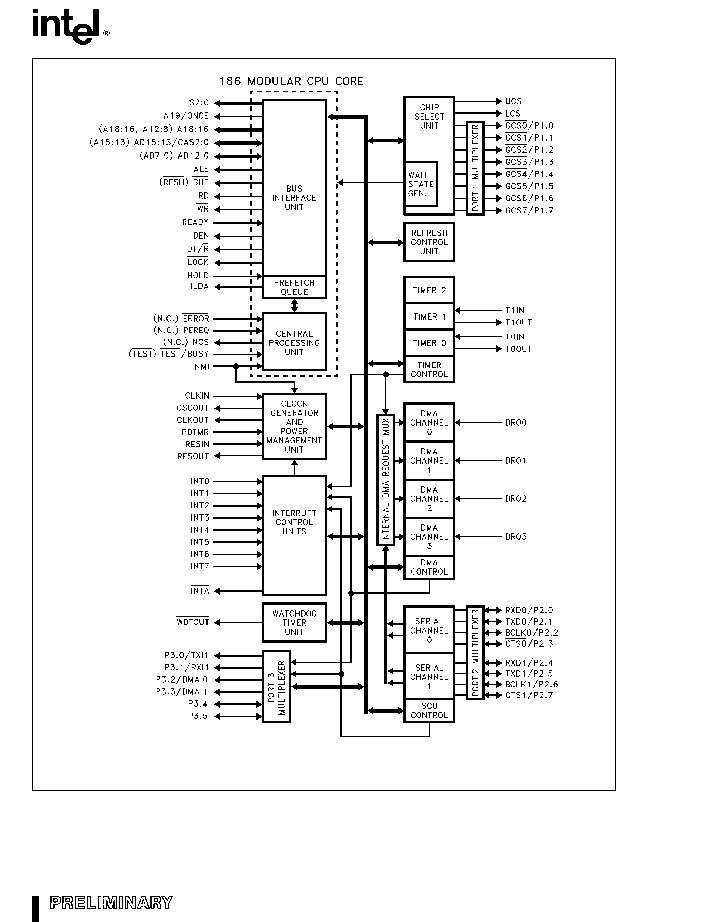
Figure 1 shows a block diagram of the 80C186EC
80C188EC The execution unit (EU) is an enhanced
8086 CPU core that includes dedicated hardware to
speed up effective address calculations enhanced
execution speed for multiple-bit shift and rotate in-
structions and for multiply and divide instructions
string move instructions that operate at full bus
bandwidth ten new instructions and fully static oper-
ation The bus interface unit (BIU) is the same as
that found on the original 186 family products ex-
cept the queue-status mode has been deleted and
buffer interface control has been changed to ease
system design timings An independent internal bus
is used for communication between the BIU and on-
chip peripherals
80C186EC CORE ARCHITECTURE
Bus Interface Unit
The 80C186EC core incorporates a bus controller
that generates local bus control signals In addition
it employs a HOLD HLDA protocol to share the local
bus with other bus masters
The bus controller is responsible for generating 20
bits of address read and write strobes bus cycle
status information and data (for write operations) in-
formation It is also responsible for reading data
from the local bus during a read operation A ready
input pin is provided to extend a bus cycle beyond
the minimum four states (clocks)
The bus controller also generates two control sig-
nals (DEN and DT R) when interfacing to external
transceiver chips This capability allows the addition
of transceivers for simple buffering of the multi-
plexed address data bus
Clock Generator
The 80C186EC provides an on-chip clock generator
for both internal and external clock generation The
clock generator features a crystal oscillator a divide-
by-two counter and three low-power operating
modes
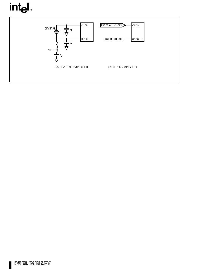
The oscillator circuit is designed to be used with ei-
ther a parallel resonant fundamental or third-over-
tone mode crystal network Alternatively the oscilla-
tor circuit may be driven from an external clock
source Figure 2 shows the various operating modes
of the oscillator circuit
The crystal or clock frequency chosen must be twice
the required processor operating frequency due to
the internal divide-by-two counter This counter is
used to drive all internal phase clocks and the exter-
nal CLKOUT signal CLKOUT is a 50% duty cycle
processor clock and can be used to drive other sys-
tem components All AC timings are referenced to
CLKOUT
The following parameters are recommended when
choosing a crystal
Temperature Range
Application Specific
ESR (Equivalent Series Res )
40X max
C0 (Shunt Capacitance of Crystal)
7 0 pF max
C
L
(Load Capacitance)
20 pF
g
2 pF
Drive Level
1 mW (max)
4

80C186EC 188EC 80L186EC 188EC
272434 ≠ 2
NOTE
1 The LC network is only required when using a third overtone crystal
Figure 2 80C186EC Clock Connections
80C186EC PERIPHERAL
ARCHITECTURE
The 80C186EC integrates several common system
peripherals with a CPU core to create a compact yet
powerful system The integrated peripherals are de-
signed to be flexbile and provide logical interconnec-
tions between supporting units (e g
the DMA unit
can accept requests from the Serial Communica-
tions Unit)
The list of integrated peripherals includes
Two cascaded 8259A compatible Programma-
ble Interrupt Controllers
3-Channel Timer Counter Unit
2-Channel Serial Communications Unit
4-Channel DMA Unit
10-Output Chip-Select Unit
32-bit Watchdog Timer Unit
I O Port Unit
Refresh Control Unit
Power Management Unit
The registers associated with each integrated pe-
ripheral are contained within a 128 x 16-bit register
file called the Peripheral Control Block (PCB) The
base address of the PCB is programmable and can
be located on any 256 byte address boundary in ei-
ther memory or I O space
Figure 3 provides a list of the registers associated
with the PCB The Register Bit Summary individually
lists all of the registers and identifies each of their
programming attributes
5


