Other brands and names are the property of their respective owners
Information in this document is provided in connection with Intel products Intel assumes no liability whatsoever including infringement of any patent or
copyright for sale and use of Intel products except as provided in Intel's Terms and Conditions of Sale for such products Intel retains the right to make
changes to these specifications at any time without notice Microcomputer Products may have minor variations to this specification known as errata
June, 2002
COPYRIGHT
© INTEL CORPORATION, 2002
Order Number: 272431-005
80C186XL 80C188XL
16-BIT HIGH-INTEGRATION EMBEDDED PROCESSORS
Y
Low Power Fully Static Versions of
80C186 80C188
Y
Operation Modes
Enhanced Mode
DRAM Refresh Control Unit
Power-Save Mode
Direct Interface to 80C187
(80C186XL Only)
Compatible Mode
NMOS 80186 80188 Pin-for-Pin
Replacement for Non-Numerics
Applications
Y
Integrated Feature Set
Static Modular CPU
Clock Generator
2 Independent DMA Channels
Programmable Interrupt Controller
3 Programmable 16-Bit Timers
Dynamic RAM Refresh Control Unit
Programmable Memory and
Peripheral Chip Select Logic
Programmable Wait State Generator
Local Bus Controller
Power-Save Mode
System-Level Testing Support (High
Impedance Test Mode)
Y
Completely Object Code Compatible
with Existing 8086 8088 Software and
Has 10 Additional Instructions over
8086 8088
Y
Speed Versions Available
25 MHz (80C186XL25 80C188XL25)
20 MHz (80C186XL20 80C188XL20)
12 MHz (80C186XL12 80C188XL12)
Y
Direct Addressing Capability to
1 MByte Memory and 64 Kbyte I O
Y
Available in 68-Pin
Plastic Leaded Chip Carrier (PLCC)
Ceramic Pin Grid Array (PGA)
Ceramic Leadless Chip Carrier
(JEDEC A Package)
Y
Available in 80-Pin
Quad Flat Pack (EIAJ)
Shrink Quad Flat Pack (SGFP)
Y
Available in Extended Temperature
Range (
b
40 C to
a
85 C)
The Intel 80C186XL is a Modular Core re-implementation of the 80C186 microprocessor It offers higher speed
and lower power consumption than the standard 80C186 but maintains 100% clock-for-clock functional com-
patibility Packaging and pinout are also identical
272431-1

80C186XL 80C188XL
16-Bit High-Integration Embedded Processors
CONTENTS
PAGE
INTRODUCTION
4
80C186XL CORE ARCHITECTURE
4
80C186XL Clock Generator
4
Bus Interface Unit
5
80C186XL PERIPHERAL
ARCHITECTURE
5
Chip-Select Ready Generation Logic
5
DMA Unit
6
Timer Counter Unit
6
Interrupt Control Unit
6
Enhanced Mode Operation
6
Queue-Status Mode
6
DRAM Refresh Control Unit
7
Power-Save Control
7
Interface for 80C187 Math Coprocessor
(80C186XL Only)
7
ONCE Test Mode
7
PACKAGE INFORMATION
8
Pin Descriptions
8
80C186XL 80C188XL Pinout
Diagrams
16
ELECTRICAL SPECIFICATIONS
22
Absolute Maximum Ratings
22
DC SPECIFICATIONS
22
Power Supply Current
23
CONTENTS
PAGE
AC SPECIFICATIONS
24
Major Cycle Timings (Read Cycle)
24
Major Cycle Timings (Write Cycle)
26
Major Cycle Timings (Interrupt
Acknowledge Cycle)
27
Software Halt Cycle Timings
28
Clock Timings
29
Ready Peripheral and Queue Status
Timings
30
Reset and Hold HLDA Timings
31
AC TIMING WAVEFORMS
36
AC CHARACTERISTICS
37
EXPLANATION OF THE AC
SYMBOLS
39
DERATING CURVES
40
80C186XL 80C188XL EXPRESS
41
80C186XL 80C188XL EXECUTION
TIMINGS
41
INSTRUCTION SET SUMMARY
42
REVISION HISTORY
48
ERRATA
48
PRODUCT IDENTIFICATION
48
2
80C186XL 80C188XL
NOTE
Pin names in parentheses applies to 80C188XL
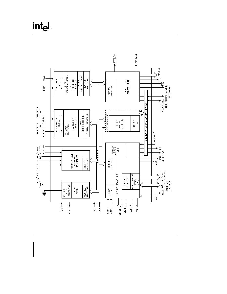
Figure 1 80C186XL 80C188XL Block Diagram
272431
≠
2
3
80C186XL 80C188XL
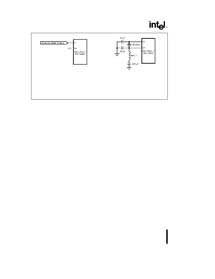
(2a)
272431 ≠ 3
272431 ≠ 4
(2b)
Note 1
XTAL Frequency
L1 Value
20 MHz
12 0 mH
g
20%
25 MHz
8 2 mH
g
20%
32 MHz
4 7 mH
g
20%
40 MHz
3 0 mH
g
20%
LC network is only required when using a third
overtone crystal
Figure 2 Oscillator Configurations (see text)
INTRODUCTION
Unless specifically noted
all references to the
80C186XL apply to the 80C188XL References to
pins that differ between the 80C186XL and the
80C188XL are given in parentheses
The following Functional Description describes the
base architecture of the 80C186XL The 80C186XL
is a very high integration 16-bit microprocessor It
combines 15 ≠ 20 of the most common microproces-
sor system components onto one chip
The
80C186XL is object code compatible with the
8086 8088 microprocessors and adds 10 new in-
struction types to the 8086 8088 instruction set
The 80C186XL has two major modes of operation
Compatible and Enhanced In Compatible Mode the
80C186XL is completely compatible with NMOS
80186 with the exception of 8087 support The En-
hanced mode adds three new features to the system
design These are Power-Save control Dynamic
RAM refresh and an asynchronous Numerics Co-
processor interface (80C186XL only)
80C186XL CORE ARCHITECTURE
80C186XL Clock Generator
The 80C186XL provides an on-chip clock generator
for both internal and external clock generation The
clock generator features a crystal oscillator a divide-
by-two counter
synchronous and asynchronous
ready inputs and reset circuitry
The 80C186XL oscillator circuit is designed to be
used either with a parallel resonant fundamental or
third-overtone mode crystal depending upon the
frequency range of the application This is used as
the time base for the 80C186XL
The output of the oscillator is not directly available
outside the 80C186XL The recommended crystal
configuration is shown in Figure 2b When used in
third-overtone mode the tank circuit is recommend-
ed for stable operation Alternately the oscillator
may be driven from an external source as shown in
Figure 2a
The crystal or clock frequency chosen must be twice
the required processor operating frequency due to
the internal divide by two counter This counter is
used to drive all internal phase clocks and the exter-
nal CLKOUT signal CLKOUT is a 50% duty cycle
processor clock and can be used to drive other sys-
tem components All AC Timings are referenced to
CLKOUT
Intel recommends the following values for crystal se-
lection parameters
Temperature Range
Application Specific
ESR (Equivalent Series Resistance)
60X max
C
0
(Shunt Capacitance of Crystal)
7 0 pF max
C
1
(Load Capacitance)
20 pF
g
2 pF
Drive Level
2 mW max
4
80C186XL 80C188XL
Bus Interface Unit
The 80C186XL provides a local bus controller to
generate the local bus control signals In addition it
employs a HOLD HLDA protocol for relinquishing
the local bus to other bus masters It also provides
outputs that can be used to enable external buffers
and to direct the flow of data on and off the local
bus
The bus controller is responsible for generating 20
bits of address read and write strobes bus cycle
status information and data (for write operations) in-
formation It is also responsible for reading data
from the local bus during a read operation Synchro-
nous and asynchronous ready input pins are provid-
ed to extend a bus cycle beyond the minimum four
states (clocks)
The 80C186XL bus controller also generates two
control signals (DEN and DT R) when interfacing to
external transceiver chips This capability allows the
addition of transceivers for simple buffering of the
multiplexed address data bus
During RESET the local bus controller will perform
the following action
Drive DEN RD and WR HIGH for one clock cy-
cle then float them
Drive S0 ≠ S2 to the inactive state (all HIGH) and
then float
Drive LOCK HIGH and then float
Float AD0 ≠ 15 (AD0 ≠ 8) A16 ≠ 19 (A9 ≠ A19) BHE
(RFSH) DT R
Drive ALE LOW
Drive HLDA LOW
RD QSMD
UCS
LCS
MCS0 PEREQ
MCS1
ERROR and TEST BUSY pins have internal pullup
devices which are active while RES is applied Ex-
cessive loading or grounding certain of these pins
causes the 80C186XL to enter an alternative mode
of operation
RD QSMD low results in Queue Status Mode
UCS and LCS low results in ONCE Mode
TEST BUSY low (and high later) results in En-
hanced Mode
80C186XL PERIPHERAL
ARCHITECTURE
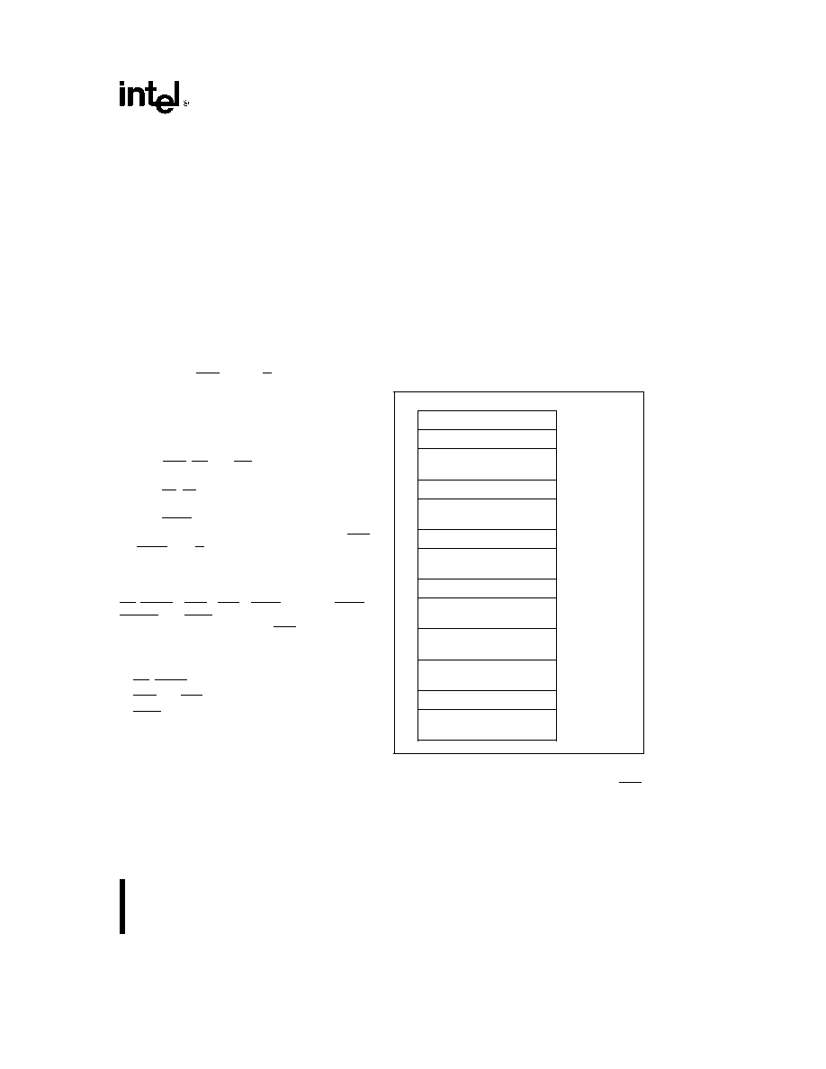
All the 80C186XL integrated peripherals are con-
trolled by 16-bit registers contained within an inter-
nal 256-byte control block The control block may be
mapped into either memory or I O space Internal
logic will recognize control block addresses and re-
spond to bus cycles An offset map of the 256-byte
control register block is shown in Figure 3
Chip-Select Ready Generation Logic
The 80C186XL contains logic which provides
programmable chip-select generation for both mem-
ories and peripherals
In addition
it can be
programmed to provide READY (or WAIT state) gen-
eration It can also provide latched address bits A1
and A2 The chip-select lines are active for all mem-
ory and I O cycles in their programmed areas
whether they be generated by the CPU or by the
integrated DMA unit
The 80C186XL provides 6 memory chip select out-
puts for 3 address areas upper memory lower
memory and midrange memory One each is provid-
ed for upper memory and lower memory while four
are provided for midrange memory
OFFSET
Relocation Register
FEH
DMA Descriptors Channel 1
DAH
D0H
DMA Descriptors Channel 0
CAH
C0H
Chip-Select Control Registers
A8H
A0H
Time 2 Control Registers
66H
60H
Time 1 Control Registers
5EH
58H
Time 0 Control Registers
56H
50H
Interrupt Controller Registers
3EH
20H
Figure 3 Internal Register Map
The 80C186XL provides a chip select called UCS
for the top of memory The top of memory is usually
used as the system memory because after reset the
80C186XL begins executing at memory location
FFFF0H
5