 | –≠–ª–µ–∫—Ç—Ä–æ–Ω–Ω—ã–π –∫–æ–º–ø–æ–Ω–µ–Ω—Ç: 80C31BH | –°–∫–∞—á–∞—Ç—å:  PDF PDF  ZIP ZIP |

Other brands and names are the property of their respective owners
Information in this document is provided in connection with Intel products Intel assumes no liability whatsoever including infringement of any patent or
copyright for sale and use of Intel products except as provided in Intel's Terms and Conditions of Sale for such products Intel retains the right to make
changes to these specifications at any time without notice Microcomputer Products may have minor variations to this specification known as errata
January 1995
COPYRIGHT
INTEL CORPORATION 1995
Order Number 270419-007
80C31BH 80C51BH 87C51
MCS
51
CHMOS SINGLE-CHIP 8-BIT MICROCONTROLLER
Automotive
Y
Extended Automotive Temperature
Range (
b
40 C to
a
125 C Ambient)
Y
High Performance CHMOS Process
Y
Power Control Modes
Y
4 Kbyte On-Chip ROM EPROM
Y
128 x 8-bit RAM
Y
32 Programmable I O Lines
Y
Two 16-Bit Timer Counters
Y
5 Interrupt Sources
Y
Quick-Pulse EPROM Programming
Y
2-Level Program Memory Lock EPROM
Y
Boolean Processor
Y
Programmable Serial Port
Y
TTL- and CMOS-Compatible Logic
Levels
Y
64K External Program Memory Space
Y
64K External Data Memory Space
Y
IDLE and POWER DOWN Modes
Y
ONCE Mode Facilitates System Testing
Y
Available in 12 MHz and 16 MHz
Versions
Y
Available in PLCC and DIP Packages
(See Packaging Specification Order
231369)
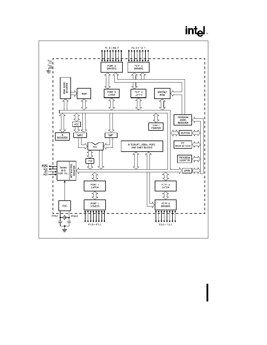
The MCS
51 CHMOS microcontroller products are fabricated on Intel's reliable CHMOS process and are
functionally compatible with the standard MCS 51 HMOS microcontroller products This technology combines
the high speed and density characteristics of HMOS with the low power attributes of CHMOS This combina-
tion expands the effectiveness of the powerful MCS 51 microcontroller architecture and instruction set
Like the MCS 51 HMOS microcontroller versions the MCS 51 CHMOS microcontroller products have the
following features 4 Kbytes of EPROM ROM (87C51 80C51BH respectively) 128 bytes of RAM 32 I O lines
two 16-bit timer counters a five-source two-level interrupt structure a full duplex serial port and on-chip
oscillator and clock circuitry In addition the MCS 51 CHMOS microcontroller products exhibit low operating
power along with two software selectable modes of reduced activity for further power reduction
Idle and
Power Down
The Idle mode freezes the CPU while allowing the RAM timer counters serial port and interrupt system to
continue functioning The Power Down mode saves the RAM contents but freezes the oscillator causing all
other chip functions to be inoperative
The 87C51 is the EPROM version of the 80C51BH It contains 4 Kbytes of on-chip program memory that can
be electrically programmed and can be erased by exposure to ultraviolet light The 87C51 EPROM array uses
a modified Quick-Pulse Programming algorithm by which the entire 4 Kbyte array can be programmed in about
12 seconds
NOTICE
This datasheet contains information on products in full production Specifications within this datasheet
are subject to change without notice Verify with your local Intel sales office that you have the latest
datasheet before finalizing a design
AUTOMOTIVE 80C31BH 80C51BH 87C51
270419 ≠ 1
Figure 1 MCS
51 Microcontroller Architectural Block Diagram
2
AUTOMOTIVE 80C31BH 80C51BH 87C51
80C31BH 80C51BH 87C51
PRODUCT OPTIONS
Intel's extended and automotive temperature range
products are designed to meet the needs of those
applications whose operating requirements exceed
commercial standards
With the extended temperature range option opera-
tional characteristics are guaranteed over the tem-
perature range of b40 C to a85 C ambient For the
automotive temperature range option operational
characteristics are guaranteed over the temperature
range of b40 C to a125 C ambient
The automotive and extended temperature versions
of the MCS 51 microcontroller product families are
available with or without burn-in options as listed in
Table 1
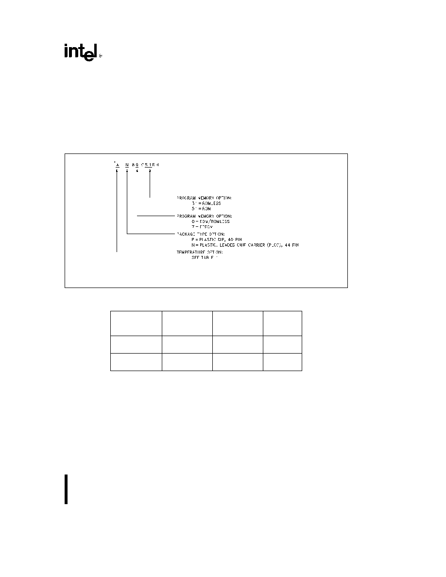
As shown in Figure 2 temperature burn-in and
package options are identified by a one- or two-letter
prefix to the part number
270419 ≠ 2
Example
AN80C51 indicates an automotive temperature range version of the 80C51 in a PLCC package with 4 Kbyte ROM
program memory
Figure 2 MCS
51 Microcontroller Product Family Nomenclature
Table 1 Temperature Options
Temperature
Temperature
Operating
Burn-In
Classification
Designation
Temperature
Options
C Ambient
Extended
T
b
40 to a85
Standard
L
b
40 to a85
Extended
Automotive
A
b
40 toa125
Standard
B
b
40 toa125
Extended
3
AUTOMOTIVE 80C31BH 80C51BH 87C51
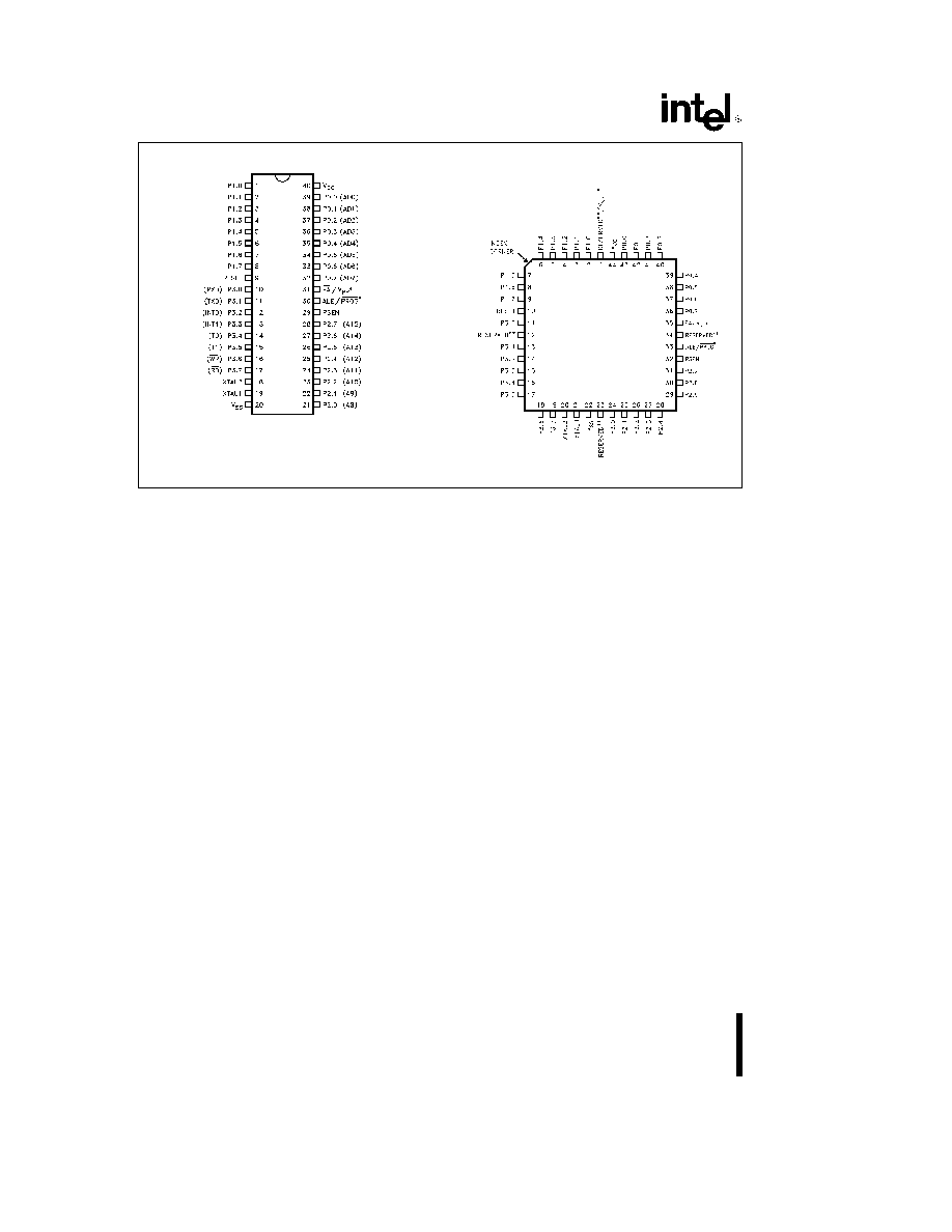
Diagrams are for pin reference only Package sizes are not to scale
270419 ≠ 3
Pin (PDIP)
EPROM only
Do not connect reserved pins
270419 ≠ 4
Pad (PLCC)
Figure 3 Pin Connections
PIN DESCRIPTION
V
CC
Supply voltage during normal Idle and Power
Down operations
V
SS
Circuit ground
V
SS1
V
SS1
(EPROM
PLCC
only)
secondary
ground Provided to reduce ground bounce and im-
prove power supply bypassing
NOTE
This pin is not a substitute for the V
SS
pin (pin 22)
For ROM and ROMless pin 1 is reserved
do not
connect
Port 0
Port 0 is an 8-bit open drain bidirectional I O
port As an output port each pin can sink 8 LS TTL
inputs Port 0 pins that have 1s written to them float
and in that state can be used as high-impedance
inputs
Port 0 is also the multiplexed low-order address and
data bus during accesses to external memory In this
application it uses strong internal pullups when emit-
ting 1s
Port 0 also receives the code bytes during EPROM
programming and outputs the code bytes during
program verification External pullups are required
during program verification
Port 1
Port 1 is an 8-bit bidirectional I O port with
internal pullups Port 1 pins that have 1s written to
them are pulled high by the internal pullups and in
that state can be used as inputs As inputs Port 1
pins that are externally being pulled low will source
current (I
IL
on the datasheet) because of the inter-
nal pullups
Port 1 also receives the low-order address bytes
during EPROM programming and program verifica-
tion
Port 2
Port 2 is an 8-bit bidirectional I O port with
internal pullups Port 2 pins that have 1s written to
them are pulled high by the internal pullups and in
that state can be used as inputs As inputs Port 2
pins that are externally being pulled low will source
current (I
IL
on the data sheet) because of the inter-
nal pullups
Port 2 emits the high-order address byte during
fetches from external Program memory and during
accesses to external Data Memory that use 16-bit
address (MOVX
DPTR) In this application it uses
strong internal pullups when emitting 1s
During accesses to external Data Memory that use
8-bit addresses (MOVX
Ri) Port 2 emits the con-
tents of the P2 Special Function Register
Port 2 also receives some control signals and the
high-order address bits during EPROM programming
and program verification
Port 3
Port 3 is an 8-bit bidirectional I O port with
internal pullups Port 3 pins that have 1s written to
them are pulled high by the internal pullups and in
that state can be used as inputs As inputs Port 3
pins that are externally being pulled low will source
current (I
IL
on the datasheet) because of the pull-
ups
4
AUTOMOTIVE 80C31BH 80C51BH 87C51
Port 3 also serves the functions of various special
features of the MCS 51 microcontroller family as
listed below
Pin
Name
Alternate Function
P3 0
RXD
Serial Input Line
P3 1
TXD
Serial Output Line
P3 2
INT0
External Interrupt 0
P3 3
INT1
External Interrupt 1
P3 4
T0
Timer 0 External Input
P3 5
T1
Timer 1 External Input
P3 6
WR
External Data Memory Write Strobe
P3 7
RD
External Data Memory Read Strobe
Port 3 also receives some control signals for
EPROM programming and program verification
RESET
Reset input A logic high on this pin for two
machine cycles while the oscillator is running resets
the device An internal pulldown resistor permits a
power-on reset to be generated using only an exter-
nal capacitor to V
CC
ALE PROG (EPROM Only)
Address Latch Enable
output signal for latching the low byte of the address
during accesses to external memory This pin is also
the program pulse input (PROG) during EPROM pro-
gramming
In normal operation ALE is emitted at a constant
rate of 1 6 the oscillator frequency and may be
used for external timing or clocking purposes Note
however that one ALE pulse is skipped during each
access to external Data Memory
PSEN
Program Store Enable is the Read strobe
to
External
Program
Memory
When
the
87C51 80C51BH is executing from Internal Program
Memory PSEN is inactive (high) When the device is
executing code from External Program Memory
PSEN is activated twice each machine cycle except
that two PSEN activations are skipped during each
access to External Data Memory
EA V
PP
External Access enable
EA must be
strapped
to
V
SS
in
order
to
enable
the
87C51 80C51BH to fetch code from External Pro-
gram Memory locations starting at 0000H up to
0FFFFH
Note however that if either of the Lock
Bits is programmed the logic level at EA is internally
latched during reset
(EPROM only )
EA must be strapped to V
CC
for internal program
execution
V
PP
(EPROM Only)
This pin also receives the
12 75V programming supply voltage (V
PP
) during
EPROM programming
270419 ≠ 5
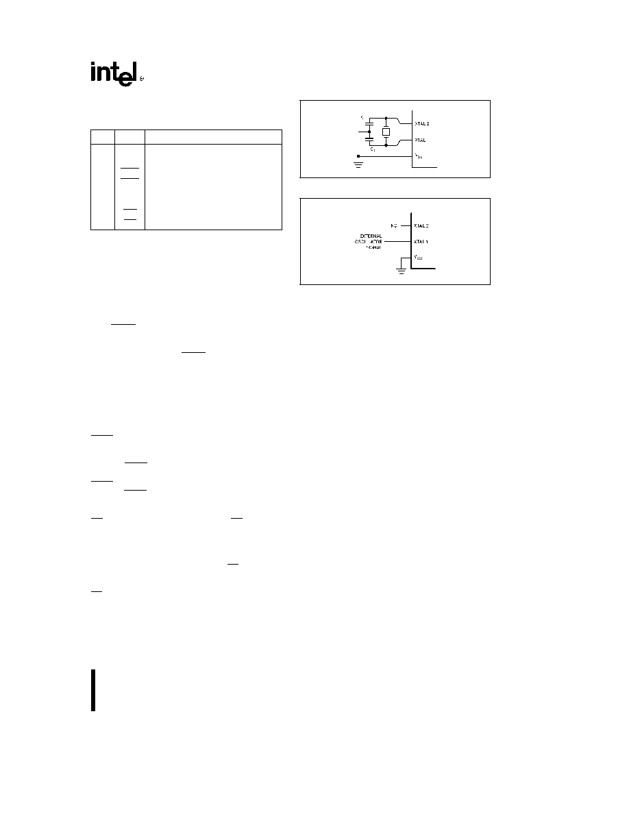
Figure 4 Using the On-Chip Oscillator
270419 ≠ 6
Figure 5 External Clock Drive
XTAL1
Input to the inverting oscillator amplifier and
input to the internal clock generating circuits
XTAL2
Output from the inverting oscillator amplifi-
er
OSCILLATOR CHARACTERISTICS
XTAL1 and XTAL2 are the input and output respec-
tively of an inverting amplifier which can be config-
ured for use as an on-chip oscillator as shown in
Figure 4
To drive the device from an external clock source
XTAL1 should be driven while XTAL2 is left uncon-
nected as shown in Figure 5 There are no require-
ments on the duty cycle of the external clock signal
since the input to the internal clocking circuitry is
through a divide-by-two flip-flop but minimum and
maximum high and low times specified on the Data-
sheet must be observed
IDLE MODE
In Idle Mode the CPU puts itself to sleep while all
the on-chip peripherals remain active The mode is
invoked by software The content of the on-chip
RAM and all the Special Functions Registers remain
unchanged during this mode The Idle Mode can be
terminated by any enabled interrupt or by a hard-
ware reset
It should be noted that when Idle is terminated by a
hardware reset the device normally resumes pro-
gram execution from where it left off up to two ma-
chine cycles before the internal reset algorithm
takes control On-chip hardware inhibits access to
5