
Other brands and names are the property of their respective owners
Information in this document is provided in connection with Intel products Intel assumes no liability whatsoever including infringement of any patent or
copyright for sale and use of Intel products except as provided in Intel's Terms and Conditions of Sale for such products Intel retains the right to make
changes to these specifications at any time without notice Microcomputer Products may have minor variations to this specification known as errata
December 1995
COPYRIGHT
INTEL CORPORATION 1996
Order Number 290474-003
82078 44 PIN
CHMOS SINGLE-CHIP FLOPPY DISK CONTROLLER
Y
Small Footprint and Low Height
Package
Y
Enhanced Power Management
Application Software Transparency
Programmable Powerdown
Command
Save and Restore Commands for
Zero-Volt Powerdown
Auto Powerdown and Wakeup
Modes
Two External Power Management
Pins
Consumes No Power While in
Powerdown
Y
Integrated Analog Data Separator
250 Kbps
300 Kbps
500 Kbps
1 Mbps
Y
Programmable Internal Oscillator
Y
Floppy Drive Support Features
Drive Specification Command
Selectable Boot Drive
Standard IBM and ISO Format
Features
Format with Write Command for
High Performance in Mass Floppy
Duplication
Y
Integrated Tape Drive Support
Standard 1 Mbps 500 Kbps
250 Kbps Tape Drives
Y
Perpendicular Recording Support for
4 MB Drives
Y
Integrated Host Disk Interface Drivers
Y
Fully Decoded Drive Select and Motor
Signals
Y
Programmable Write Precompensation
Delays
Y
Addresses 256 Tracks Directly
Supports Unlimited Tracks
Y
16 Byte FIFO
Y
Single-Chip Floppy Disk Controller
Solution for Portables and Desktops
100% PC AT Compatible
Fully Compatible with Intel386
TM
SL
Integrated Drive and Data Bus
Buffers
Y
Separate 5 0V and 3 3V Versions of the
44 Pin part are Available
Y
Available in a 44 Pin QFP Package
The 82078 a 24 MHz crystal a resistor package and a device chip select implements a complete solution All
programmable options default to 82078 compatible values The dual PLL data separator has better perform-
ance than most board level discrete PLL implementations The FIFO allows better system performance in
multi-master (e g Microchannel EISA)
The 82078 maintains complete software compatibility with the 82077SL 82077AA 8272A floppy disk control-
lers It contains programmable power management features while integrating all of the logic required for floppy
disk control The power management features are transparent to any application software
The 82078 is fabricated with Intel's advanced CHMOS III technology and is also available in a 64-lead QFP
package
Other brands and names are the property of their respective owners

82078 44 Pin CHMOS Single-Chip Floppy Disk Controller
CONTENTS
PAGE
1 0 INTRODUCTION
8
2 0 MICROPROCESSOR INTERFACE
9
2 1 Status Data and Control
Registers
9
2 1 1 Status Register B (SRB
EREG EN
e
1)
9
2 1 2 Digital Output Register
(DOR)
10
2 1 3 Enhanced Tape Drive
Register (TDR)
11
2 1 4 Datarate Select Register
(DSR)
11
2 1 5 Main Status Register
(MSR)
13
2 1 6 FIFO (DATA)
13
2 1 7 Digital Input Register (DIR)
14
2 2 Reset
14
2 2 1 Reset Pin (``HARDWARE'')
Reset
14
2 2 2 DOR Reset vs DSR Reset
(``SOFTWARE'' RESET)
14
2 3 DMA Transfers
14
3 0 DRIVE INTERFACE
14
3 1 Cable Interface
14
3 2 Host and FDD Interface Drivers
15
3 3 Data Separator
15
3 3 1 Jitter Tolerance
16
3 3 2 Locktime (t
LOCK
)
16
3 3 3 Capture Range
16
3 4 Write Precompensation
16
CONTENTS
PAGE
4 0 POWER MANAGEMENT
FEATURES
17
4 1 Power Management Scheme
17
4 2 Oscillator Power Management
17
4 3 Part Power Management
18
4 3 1 Direct Powerdown
18
4 3 2 Auto Powerdown
18
4 3 3 Wake Up Modes
18
4 3 3 1 Wake Up from DSR
Powerdown
18
4 3 3 2 Wake Up from Auto
Powerdown
18
4 4 Register Behavior
19
4 5 Pin Behavior
19
4 5 1 System Interface Pins
19
4 5 2 FDD Interface Pins
20
5 0 CONTROLLER PHASES
20
5 1 Command Phase
20
5 2 Execution Phase
21
5 2 1 Non-DMA Mode Transfers
from the FIFO to the Host
21
5 2 2 Non-DMA Mode Transfers
from the Host to the FIFO
21
5 2 3 DMA Mode Transfers from
the FIFO to the Host
21
5 2 4 DMA Mode Transfers from
the Host to the FIFO
21
5 2 5 Data Transfer Termination
22
5 3 Result Phase
22
2

CONTENTS
PAGE
6 0 COMMAND SET DESCRIPTIONS
22
6 1 Data Transfer Commands
34
6 1 1 Read Data
34
6 1 2 Read Deleted Data
35
6 1 3 Read Track
35
6 1 4 Write Data
36
6 1 5 Write Deleted Data
36
6 1 6 Verify
36
6 1 7 Format Track
37
6 1 7 1 Format Fields
38
6 2 Scan Commands
38
6 3 Control Commands
39
6 3 1 Read ID
39
6 3 2 Recalibrate
39
6 3 3 Drive Specification
Command
39
6 3 4 Seek
40
6 3 5 Sense Interrupt Status
40
6 3 6 Sense Drive Status
41
6 3 7 Specify
41
6 3 8 Configure
41
6 3 9 Version
42
6 3 10 Relative Seek
42
6 3 11 DUMPREG
43
6 3 12 Perpendicular Mode
Command
43
6 3 12 1 About Perpendicular
Recording Mode
43
6 3 12 2 The Perpendicular
Mode Command
43
6 3 13 Powerdown Mode
Command
44
6 3 14 Part ID Command
44
6 3 15 Option Command
44
6 3 16 Save Command
44
6 3 17 Restore Command
44
6 3 18 Format and Write
Command
45
6 3 19 Lock
45
CONTENTS
PAGE
7 0 STATUS REGISTER ENCODING
46
7 1 Status Register 0
46
7 2 Status Register 1
46
7 3 Status Register 2
47
7 4 Status Register 3
47
8 0 COMPATIBILITY
48
8 1 Compatibility with the FIFO
48
8 2 Drive Polling
48
9 0 PROGRAMMING GUIDELINES
48
9 1 Command and Result Phase
Handshaking
49
9 2 Initialization
49
9 3 Recalibrates and Seeks
51
9 4 Read Write Data Operations
51
9 5 Formatting
53
9 6 Save and Restore
54
9 7 Verifies
55
9 8 Powerdown State and Recovery
55
9 8 1 Oscillator Power
Management
55
9 8 2 Part Power Management
55
9 8 2 1 Powerdown Modes
55
9 8 2 2 Wake Up Modes
56
10 0 DESIGN APPLICATIONS
56
10 1 Operating the 82078-3 in a 3 3V
Design
56
10 2 Selectable Boot Drive
58
10 3 How to Disable the Native Floppy
Contoller on the Motherboard
59
10 4 Replacing the 82077SL with a
82078 in a 5 0V Design
59
11 0 D C SPECIFICATIONS
62
11 1 Absolute Maximum Ratings
62
11 2 D C Characteristics
62
11 3 Oscillator
63
12 0 A C SPECIFICATIONS
64
12 1 Package Outline for the 44-Pin
QFP Part
70
13 0 REVISION HISTORY
71
3
82078 44 PIN
290474 � 1
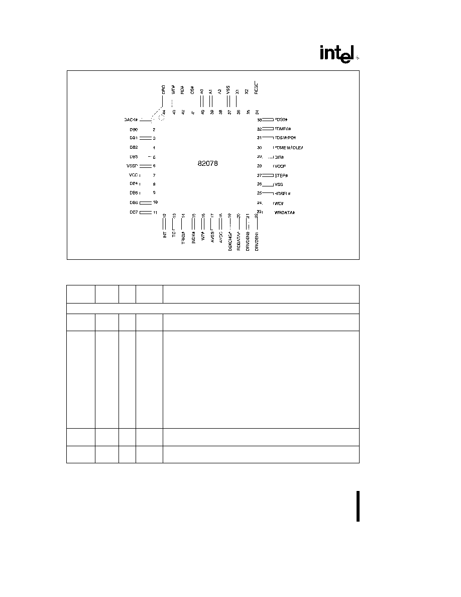
Figure 1-0 82078 44 Pin Pinout
Table 1 0 82078 (44 Pin) Description
Symbol
Pin
I O
H W
Description
Reset
HOST INTERFACE
RESET
34
I
N A
RESET
A high level places the 82078 in a known idle state All
registers are cleared except those set by the Specify command
A0
40
I
N A
ADDRESS
Selects one of the host interface registers
A1
39
A2
A1
A0
Access
Register
A2
38
0
0
0
R
Reserved
0
0
1
R W
Status Register B
SRB
0
1
0
R W
Digital Output Register
DOR
0
1
1
R W
Tape Drive Register
TDR
1
0
0
R
Main Status Register
MSR
1
0
0
W
Data Rate Select Register
DSR
1
0
1
R W
Data Register (FIFO)
FIFO
1
1
0
Reserved
1
1
1
R
Digital Input Register
DIR
1
1
1
W
Configuration Control Register
CCR
CS
41
I
N A
CHIP SELECT
Decodes the base address range and qualifies RD
and WR
RD
42
I
N A
READ
Read control signal for data transfers from the floppy drive to
the system
4
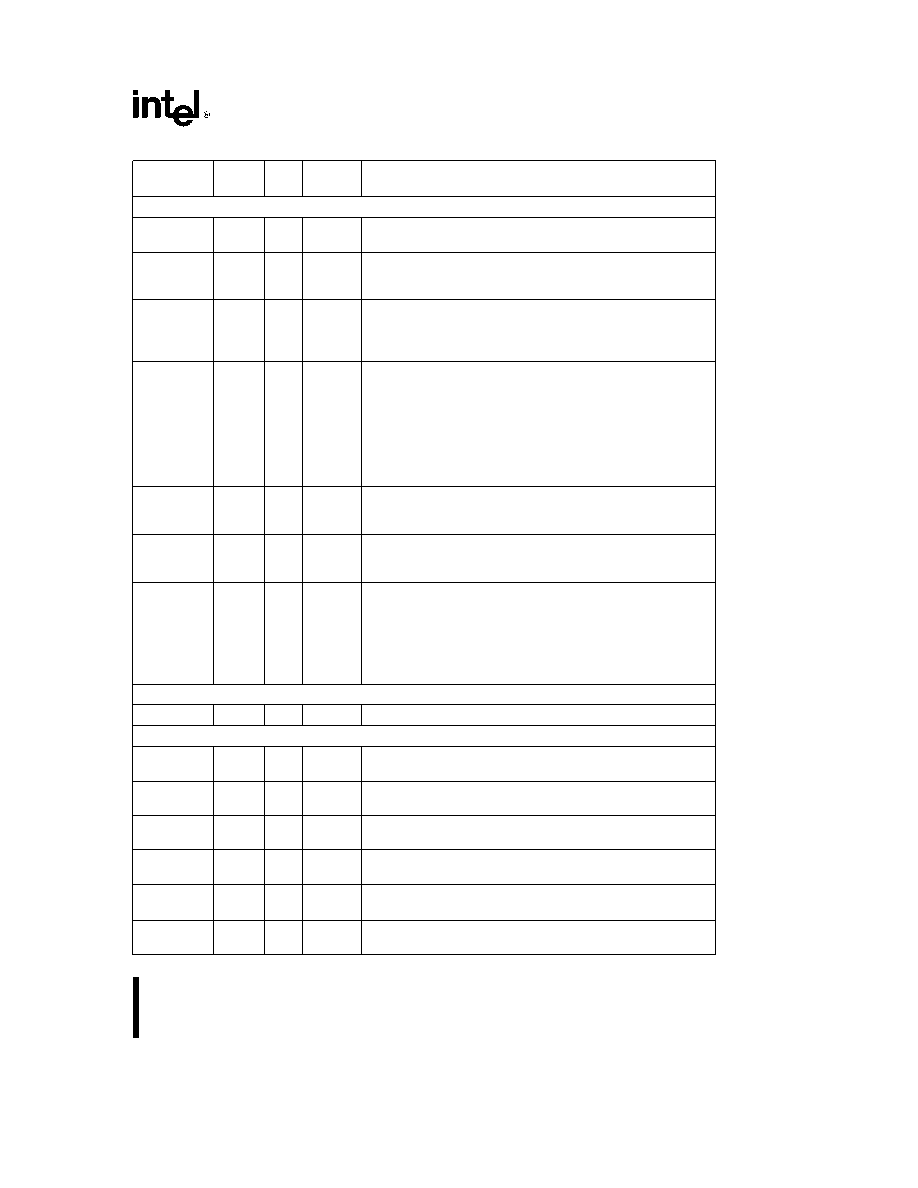
82078 44 PIN
Table 1 0 82078 (44 Pin) Description
(Continued)
Symbol
Pin
I O
H W
Description
Reset
HOST INTERFACE
(Continued)
WR
43
I
N A
WRITE
Write control signal for data transfers to the floppy
drive from the system
DRQ
44
O
DMA REQUEST
Requests service from a DMA controller
Normally active high but will go to high impedance in AT and
Model 30 modes when the appropriate bit is set in the DOR
DACK
1
I
N A
DMA ACKNOWLEDGE
Control input that qualifies the RD
WR
inputs in DMA cycles Normally active low but is disabled
in AT and Model 30 modes when the appropriate bit is set in the
DOR
DB0
2
I O
DATA BUS
12 mA data bus
DB1
3
DB2
4
DB3
5
DB4
8
DB5
9
DB6
10
DB7
11
INT
12
O
INTERRUPT
Signals a data transfer in non-DMA mode and
when status is valid Normally active high but goes to high
impedance when the appropriate bit is set in the DOR
TC
13
I
N A
TERMINAL COUNT
Control line from a DMA controller that
terminates the current disk transfer TC is effective only when
qualified by DACK
This input is active high
X1
36
N A
EXTERNAL CLOCK OR CRYSTAL
Connection for a 24 MHz
fundamental mode parallel resonant crystal X1 can also be
X2
35
driven by an external clock (external oscillator) which can be
either at 48 MHz or 24 MHz If external oscillator is used then
the PDOSC bit can be set to turn off the internal oscillator Also
if a 48 MHz external oscillator is used then the CLK48 bit must
be set in the enhanced CONFIGURE command
PLL SECTION
RDDATA
20
I
N A
READ DATA
Serial data from the floppy disk
DISK CONTROL
TRK0
14
I
N A
TRACK0
This is an active low signal that indicates that the
head on track 0
INDX
15
I
N A
INDEX
This is an active low signal that indicates the beginning
of the track
WP
16
I
N A
WRITE PROTECT
This is an active low signal that indicates
whether the floppy disk in the drive is write protected
DSKCHG
19
I
N A
DISK CHANGE
This is an input from the floppy drive reflected
in the DIR
DRVDEN0
21
O
DRIVE DENSITY
These signals are used by the floppy drive to
configure the drive for the appropriate media
DRVDEN1
22
WRDATA
23
O
WRITE DATA
MFM serial data to the drive Precompensation
value is selectable through software
5