 | –≠–ª–µ–∫—Ç—Ä–æ–Ω–Ω—ã–π –∫–æ–º–ø–æ–Ω–µ–Ω—Ç: 82371SB | –°–∫–∞—á–∞—Ç—å:  PDF PDF  ZIP ZIP |

E
© INTEL CORPORATION 1996, 1997
April 1997
Order Number: 290550-002
n
Bridge Between the PCI Bus and ISA Bus
n
PCI and ISA Master/Slave Interface
PCI from 25≠33 MHz
ISA from 7.5≠8.33 MHz
5 ISA Slots
n
Fast IDE Interface
Supports PIO and Bus Master IDE
Supports up to Mode 4 Timings
Transfer Rates to 22 MB/Sec
8 x 32-Bit Buffer for Bus Master IDE PCI
Burst Transfers
Separate Master/Slave IDE Mode
Support (PIIX3)
n
Plug-n-Play Port for Motherboard Devices
2 Steerable DMA Channels (PIIX Only)
Fast DMA with 4-Byte Buffer (PIIX Only)
2 Steerable Interrupts Lines on the PIIX
and 1 Steerable Interrupt Line on the
PIIX3
1 Programmable Chip Select
n
Steerable PCI Interrupts for PCI Device Plug-
n-Play
n
PCI Specification Revision 2.1 Compliant
(PIIX3)
n
Functionality of One 82C54 Timer
System Timer; Refresh Request;
Speaker Tone Output
n
Two 82C59 Interrupt Controller Functions
14 Interrupts Supported
Independently Programmable for
Edge/Level Sensitivity
n
Enhanced DMA Functions
Two 8237 DMA Controllers
Fast Type F DMA
Compatible DMA Transfers
7 Independently Programmable
Channels
n
X-Bus Peripheral Support
Chip Select Decode
Controls Lower X-Bus Data Byte
Transceiver
n
I/O Advanced Programmable Interrupt
Controller (IOAPIC) Support (PIIX3)
n
Universal Serial Bus (USB) Host Controller
(PIIX3)
Compatible with Universal Host
Controller Interface (UHCI)
Contains Root Hub with 2 USB Ports
n
System Power Management (Intel SMM
Support)
Programmable System Management
Interrupt (SMI)--Hardware Events,
Software Events, EXTSMI#
Programmable CPU Clock Control
(STPCLK#)
Fast On/Off Mode
n
Non-Maskable Interrupts (NMI)
PCI System Error Reporting
n
NAND Tree for Board-Level ATE Testing
n
208-Pin QFP
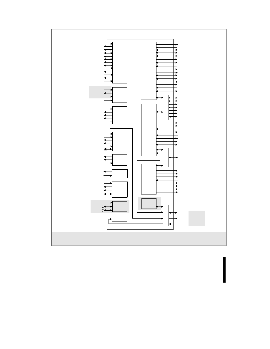
The 82371FB (PIIX) and 82371SB (PIIX3) PCI ISA IDE Xcelerators are multi-function PCI devices
implementing a PCI-to-ISA bridge function and an PCI IDE function. In addition, the PIIX3 implements a
Universal Serial Bus host/hub function. As a PCI-to-ISA bridge, the PIIX/PIIX3 integrates many common I/O
functions found in ISA-based PC systems--a seven-channel DMA controller, two 82C59 interrupt controllers,
an 8254 timer/counter, and power management support. In addition to compatible transfers, each DMA
channel supports type F transfers. Chip select decoding is provided for BIOS, real time clock, and keyboard
controller. Edge/Level interrupts and interrupt steering are supported for PCI plug and play compatibility. The
PIIX/PIIX3 supports two IDE connectors for up to four IDE devices providing an interface for IDE hard disks
and CD ROMs. The PIIX/PIIX3 provides motherboard plug and play compatibility. PIIX implements two
steerable DMA channels (including type F transfers) and up to two steerable interrupt lines. PIIX3 implements
one steerable interrupt line. The interrupt lines can be routed to any of the available ISA interrupts. Both
PIIX/PIIX3 implement a programmable chip select.
PIIX3 contains a Universal Serial Bus (USB) Host Controller that is UHCI compatible. The Host Controller's
root hub has two programmable USB ports. PIIX3 also provides support for an external IOAPIC.
This document describes the PIIX3 Component. Unshaded areas describe the 82371FB PIIX. Shaded areas,
like this one, describe the PIIX3 operations that differ from the 82371FB PIIX.
82371FB (PIIX) AND 82371SB (PIIX3)
PCI ISA IDE XCELERATOR
82371FB (PIIX) AND 82371SB (PIIX3)
E
2
USBP1
USBP0
PCI
Bus
Interface
ISA
Bus
Interface
Mother
Board
Interface
Interrupt
Timers/
Counters
DMA
PCICLK
AD[31:0]
C/BE[3:0]#
FRAME#
IRDY#
TRDY#
STOP#
DEVSEL#
SERR#
PAR
IDSEL
MIRQ1
MDRQ[1:0]
MDAK[1:0]#
INTR
NMI
IRQ(15,14,11:9,7:3,1)
DACK[7:5,3:0]#
TC
REFRESH#
SD[15:0]
LA23/CS1S
IOCS16#
MEMCS16#
DD12/SBHE#
MEMR#
MEMW#
AEN
IOCHRDY
IOCHK#
SYSCLK
BALE
IOR#
IOW#
SMEMR#
SMEMW#
ZEROWS#
blkdia.drw
SPKR
FERR#
IGNNE#
X-Bus
Support
Logic
OSC
IRQ12/M
IRQ8#
Test
TESTIN# or APICREQ#
PIRQ[A:D]#
SMI#
STPCLK#
EXTSMI#
System
Power
Mgmt
PHOLD#
PHOLDA#
System
Reset
PWROK
CPURST
PCIRST# or APICACK#
RSTDRV
INIT
IDE
Interface
SA[7:0]
DD[11:0]/SA[19:8]
M
U
X
LA22/CS3S
LA21/CS1P
LA20/CS3P
LA19:17]/DA[2:0]
DIOR#
DIOW#
DDRQ[1:0]
DDAK[1:0]#
IORDY
SOE#
SDIR
DD15/PCS#
M
U
X
XDIR#
XOE#
RTCALE
BIOSCS#
RTCCS#
KBCS#
DD13
DREQ[7:5,3:0]
I/O APIC
Support
Logic
M
U
X
DD14
PCIRST#
TESTIN#
DD14 or APICCS#
Universial
Serial
Interface
USBCLK
PIIX Only
(Not On PIIX3)
MIRQ0
PIIX3 Only
(Not On PIIX)
PIIX3 Only
(Not On PIIX)
Note:
1.
IOAPIC signals are multiplexed with signals from the System Reset, Test, and IDE Interface blocks
2.
PIRQD# is an input on the PIIX and bi-directional on PIIX3.
PIIX/PIIX3 Simplified Block Diagram

E
82371FB (PIIX) AND 82371SB (PIIX3)
3
CONTENTS
PAGE
REVISION HISTORY...................................................................................................................................... 7
1.0. SIGNAL DESCRIPTION .......................................................................................................................... 9
1.1. PCI Interface Signals ........................................................................................................................... 9
1.2. Motherboard I/O Device Interface Signals .......................................................................................... 10
1.3. IDE Interface Signals ......................................................................................................................... 11
1.4. ISA Interface Signals.......................................................................................................................... 13
1.5. DMA Signals ...................................................................................................................................... 15
1.6. Timer/Counter Signals........................................................................................................................ 15
1.7. Interrupt Controller Signals................................................................................................................. 16
1.8. System Power Management (SMM) Signals ...................................................................................... 16
1.9. X-Bus Signals .................................................................................................................................... 17
1.10. APIC Bus Signals (PIIX3 Only) ........................................................................................................ 18
1.11. Universal Serial Bus Signals (PIIX3 Only) ........................................................................................ 19
1.12. System Reset Signals ...................................................................................................................... 19
1.13. Test Signals ..................................................................................................................................... 20
1.14. Power and Ground Signals............................................................................................................... 20
1.15. Signal State During Reset ................................................................................................................ 21
2.0. REGISTER DESCRIPTION ................................................................................................................... 22
2.1. Register Access ................................................................................................................................. 22
2.2. PCI Configuration Registers--PCI To ISA Bridge (Function 0)........................................................... 31
2.2.1. VID--VENDOR IDENTIFICATION REGISTER (Function 0)........................................................ 31
2.2.2. DID--DEVICE IDENTIFICATION REGISTER (Function 0) ......................................................... 31
2.2.3. PCICMD--COMMAND REGISTER (Function 0) ......................................................................... 31
2.2.4. PCISTS--PCI DEVICE STATUS REGISTER (Function 0) .......................................................... 32
2.2.5. RID--REVISION IDENTIFICATION REGISTER (Function 0)...................................................... 33
2.2.6. CLASSC
CLASS CODE REGISTER (Function 0)..................................................................... 33
2.2.7. HEDT--HEADER TYPE REGISTER (Function 0) ....................................................................... 33
2.2.8. IORT--ISA I/O RECOVERY TIMER REGISTER (Function 0) ..................................................... 33
2.2.9. XBCS--X-BUS CHIP SELECT REGISTER (Function 0) ............................................................. 34
2.2.10. PIRQRC[A:D]--PIRQx ROUTE CONTROL REGISTERS (Function 0)...................................... 36
2.2.11. TOM--TOP OF MEMORY REGISTER (Function 0).................................................................. 36
2.2.12. MSTAT--MISCELLANEOUS STATUS REGISTER (Function 0)............................................... 37
2.2.13. MBIRQ[1:0]--MOTHERBOARD DEVICE IRQ ROUTE CONTROL REGISTERS (Function 0) .. 39
2.2.14. MBDMA[1:0]--MOTHERBOARD DEVICE DMA CONTROL REGISTERS (Function 0) ............ 40
2.2.15. PCSC--PROGRAMMABLE CHIP SELECT CONTROL REGISTER (Function 0) ..................... 40
2.2.16. APICBASE--APIC BASE ADDRESS RELOCATION REGISTER (Function 0) (PIIX3 Only) ..... 41
2.2.17. DLC--DETERMINISTIC LATENCY CONTROL REGISTER (Function 0) (PIIX3 Only) ............. 42
2.2.18. SMICNTL--SMI CONTROL REGISTER (Function 0)................................................................ 43

82371FB (PIIX) AND 82371SB (PIIX3)
E
4
2.2.19. SMIEN--SMI ENABLE REGISTER (Function 0) ....................................................................... 43
2.2.20. SEE--SYSTEM EVENT ENABLE REGISTER (Function 0) ...................................................... 44
2.2.21. FTMR--FAST OFF TIMER REGISTER (Function 0)................................................................. 45
2.2.22. SMIREQ--SMI REQUEST REGISTER (Function 0) ................................................................. 45
2.2.23. CTLTMR--CLOCK SCALE STPCLK# LOW TIMER (Function 0) .............................................. 46
2.2.24. CTHTMR--CLOCK SCALE STPCLK# HIGH TIMER (Function 0)............................................. 47
2.3. PCI Configuration Registers--IDE Interface (Function 1) ................................................................... 47
2.3.1. VID--Vendor Identification Register (Function 1) ........................................................................ 47
2.3.2. DID--DEVICE IDENTIFICATION REGISTER (Function 1) ......................................................... 47
2.3.3. PCICMD--COMMAND REGISTER (Function 1) ......................................................................... 48
2.3.4. PCISTS--PCI DEVICE STATUS REGISTER (Function 1) .......................................................... 48
2.3.5. RID--REVISION IDENTIFICATION REGISTER (Function 1)...................................................... 49
2.3.6. CLASSC
CLASS CODE REGISTER (Function 1)..................................................................... 49
2.3.7. MLT--MASTER LATENCY TIMER REGISTER (Function 1) ...................................................... 49
2.3.8. HEDT--HEADER TYPE REGISTER (Function 1) ....................................................................... 50
2.3.9. BMIBA--BUS MASTER INTERFACE BASE ADDRESS REGISTER (Function 1) ...................... 50
2.3.10. IDETIM--IDE TIMING REGISTER (Function 1) ........................................................................ 51
2.3.11. SIDETIM--SLAVE IDE TIMING REGISTER (Function 1) (PIIX3 Only) ..................................... 52
2.4. PCI Configuration Registers
Universal Serial Bus (Function 2) (PIIX3 Only).................................... 53
2.4.1. VID--VENDOR IDENTIFICATION REGISTER (Function 2) (PIIX3)............................................ 53
2.4.2. DID
DEVICE IDENTIFICATION REGISTER (Function 2) (PIIX3) ............................................. 54
2.4.3. PCICMD
COMMAND REGISTER (Function 2) (PIIX3) ............................................................. 54
2.4.4. DS
DEVICE STATUS REGISTER (Function 2) (PIIX3)............................................................. 55
2.4.5. RID
REVISION IDENTIFICATION REGISTER (Function 2) (PIIX3).......................................... 55
2.4.6. CLASSC
CLASS CODE REGISTER (Function 2) (PIIX3)......................................................... 56
2.4.7. MLT
MASTER LATENCY TIMER REGISTER (Function 2) (PIIX3) .......................................... 56
2.4.8. HEDT
HEADER TYPE REGISTER (Function 2) (PIIX3) ........................................................... 57
2.4.9. BASEADD
I/O SPACE BASE ADDRESS (Function 2) (PIIX3) ................................................ 57
2.4.10. IL
Interrupt Line Register (Function 2) (PIIX3)......................................................................... 57
2.4.11. INTRP
INTERRUPT PIN (Function 2) (PIIX3) ......................................................................... 58
2.4.12. SBRNUM
SERIAL BUS RELEASE NUMBER (Function 2) (PIIX3) ......................................... 58
2.4.13. MSTAT
MISCELLANEOUS STATUS REGISTER (Function 2) (PIIX3)................................... 58
2.4.14. LEGSUP
LEGACY SUPPORT REGISTER (FUNCTION 2) (PIIX3) ........................................ 59
2.5. ISA-Compatible Registers .................................................................................................................. 61
2.5.1. DMA REGISTERS....................................................................................................................... 61
2.5.1.1. DCOM--DMA Command Register........................................................................................ 61
2.5.1.2. DCM--DMA Channel Mode Register.................................................................................... 61
2.5.1.3. DR--DMA Request Register................................................................................................. 62
2.5.1.4. Mask Register--Write Single Mask Bit ................................................................................. 63
2.5.1.5. Mask Register--Write All Mask Bits...................................................................................... 63
2.5.1.6. DS--DMA Status Register .................................................................................................... 64
2.5.1.7. DMA Base And Current Address Registers (8237 Compatible Segment).............................. 64
2.5.1.8. DMA Base And Current Byte/Word Count Registers (Compatible Segment) ........................ 65

E
82371FB (PIIX) AND 82371SB (PIIX3)
5
2.5.1.9. DMA Memory Low Page Registers ....................................................................................... 65
2.5.1.10. DMA Clear Byte Pointer Register........................................................................................ 66
2.5.1.11. DMC--DMA Master Clear Register..................................................................................... 66
2.5.1.12. DCLM--DMA Clear Mask Register ..................................................................................... 66
2.5.2. TIMER/COUNTER REGISTER DESCRIPTION .......................................................................... 66
2.5.2.1. TCW--Timer Control Word Register..................................................................................... 66
2.5.2.2. Interval Timer Status Byte Format Register .......................................................................... 68
2.5.2.3. Counter Access Ports Register ............................................................................................. 69
2.5.3. INTERRUPT CONTROLLER REGISTERS ................................................................................. 69
2.5.3.1. ICW1--Initialization Command Word 1 Register................................................................... 70
2.5.3.2. ICW2--Initialization Command Word 2 Register................................................................... 70
2.5.3.3. ICW3--Initialization Command Word 3 Register................................................................... 71
2.5.3.4. ICW3--Initialization Command Word 3 Register................................................................... 71
2.5.3.5. ICW4--Initialization Command Word 4 Register................................................................... 71
2.5.3.6. OCW1--Operational Control Word 1 Register ...................................................................... 72
2.5.3.7. OCW2--Operational Control Word 2 Register ...................................................................... 72
2.5.3.8. OCW3--Operational Control Word 3 Register ...................................................................... 73
2.5.3.9. ELCR1--Edge/Level Triggered Register............................................................................... 74
2.5.3.10. ELCR2--Edge/Level Triggered Register............................................................................. 74
2.5.4. X-BUS, COPROCESSOR, and RESET REGISTERS ................................................................. 75
2.5.4.1. Reset X-Bus IRQ12 And IRQ1 Register................................................................................ 75
2.5.4.2. Coprocessor Error Register .................................................................................................. 75
2.5.4.3. RC--Reset Control Register ................................................................................................. 75
2.5.5. NMI REGISTERS ........................................................................................................................ 76
2.5.5.1. NMISC--NMI Status And Control Register ........................................................................... 76
2.5.5.2. NMI Enable and Real-Time Clock Address Register ............................................................. 77
2.6. System Power Management Registers .............................................................................................. 77
2.6.1. APMC--ADVANCED POWER MANAGEMENT CONTROL PORT ............................................. 77
2.6.2. APMS--ADVANCED POWER MANAGEMENT STATUS PORT ................................................ 78
2.7. PCI BUS Master IDE Registers .......................................................................................................... 78
2.7.1. BMICOM--BUS MASTER IDE COMMAND REGISTER ............................................................. 78
2.7.2. BMISTA--BUS MASTER IDE STATUS REGISTER ................................................................... 79
2.7.3. BMIDTP--BUS MASTER IDE DESCRIPTOR TABLE POINTER REGISTER ............................. 80
2.8. USB I/O Registers.............................................................................................................................. 80
2.8.1. USBCMD
USB Command Register........................................................................................... 80
2.8.2. USBSTS
USB Status Register .................................................................................................. 82
2.8.3. USBINTR
USB Interrupt Enable Register ................................................................................. 83
2.8.4. FRNUM
Frame Number Register .............................................................................................. 83
2.8.5. FLBASEADD
Frame List Base Address Register...................................................................... 84
2.8.6. Start Of Frame (SOF) Modify Register ........................................................................................ 84
2.8.7. PORTSC
Port Status and Control Register ............................................................................... 85
3.0. FUNCTIONAL DESCRIPTION .............................................................................................................. 89