 | –≠–ª–µ–∫—Ç—Ä–æ–Ω–Ω—ã–π –∫–æ–º–ø–æ–Ω–µ–Ω—Ç: 82438FX | –°–∫–∞—á–∞—Ç—å:  PDF PDF  ZIP ZIP |

November 1996
Order Number 290518-002
82430FX PCIset DATASHEET 82437FX
SYSTEM CONTROLLER (TSC) AND
82438FX DATA PATH UNIT (TDP)
Y
Supports all 3V Pentium
Processors
Y
Integrated Second Level Cache
Controller
Direct Mapped Organization
Write-Back Cache Policy
Cacheless 256-Kbyte and 512-Kbyte
Standard Burst and Pipelined Burst
SRAMs
Cache Hit Read Write Cycle Timings
at 3-1-1-1 with Burst or Pipelined
Burst SRAMs
Back-to-Back Read Cycles at 3-1-1-1-
1-1-1-1 with Burst or Pipelined Burst
SRAMs
Integrated Tag Valid Status Bits for
Cost Savings and Performance
Supports 5V SRAMs for Tag Address
Y
Integrated DRAM Controller
64-Bit Data Path to Memory
4 Mbytes to 128 Mbytes Main
Memory
EDO Hyper Page Mode DRAM
(x-2-2-2 Reads) or Standard Page
Mode DRAMs
5 RAS Lines
4 Qword Deep Buffer for 3-1-1-1
Posted Write Cycles
Symmetrical and Asymmetrical
DRAMs
3V or 5V DRAMs
Y
EDO DRAM Support
Highest Performance with Burst or
Pipelined Burst SRAMs
Superior Cacheless Designs
Y
Fully Synchronous 25 30 33 MHz PCI
Bus Interface
100 MB s Instant Access Enables
Native Signal Processing (NSP) on
Pentium Processors
Synchronized CPU-to-PCI Interface
for High Performance Graphics
PCI Bus Arbiter PIIX and Four PCI
Bus Masters Supported
CPU-to-PCI Memory Write Posting
with 4 Dword Deep Buffers
Converts Back-to-Back Sequential
CPU to PCI Memory Writes to PCI
Burst Writes
PCI-to-DRAM Posting of 12 Dwords
PCI-to-DRAM up to 120 Mbytes Sec
Bandwidth Utilizing Snoop Ahead
Feature
Y
NAND Tree for Board-Level ATE
Testing
Y
208 Pin QFP for the 82437FX System
Controller (TSC) 100 Pin QFP for Each
82438FX Data Path (TDP)
Y
Supported Kits
82437FX ISA Kit (TSC TDPs PIIX)
The 82430FX PCIset consists of the 82437FX System Controller (TSC) two 82438FX Data Paths (TDP) and
the 82371FB PCI ISA IDE Xcelerator (PIIX) The PCIset forms a Host-to-PCI bridge and provides the second
level cache control and a full function 64-bit data path to main memory The TSC integrates the cache and
main memory DRAM control functions and provides bus control for transfers between the CPU cache main
memory and the PCI Bus The second level (L2) cache controller supports a write-back cache policy for cache
sizes of 256 Kbytes and 512 Kbytes Cacheless designs are also supported The cache memory can be
implemented with either standard burst or pipelined burst SRAMs An external Tag RAM is used for the
address tag and an internal Tag RAM for the cache line status bits For the TSC's DRAM controller five rows
are supported for up to 128 Mbytes of main memory The TSC's optimized PCI interface allows the CPU to
sustain the highest possible bandwidth to the graphics frame buffer at all frequencies Using the snoop ahead
feature the TSC allows PCI masters to achieve full PCI bandwidth The TDPs provide the data paths between
the CPU cache main memory and PCI For increased system performance the TDPs contain read prefetch
and posted write buffers
82437FX TSC AND 82438FX TDP
290518 ≠ 1
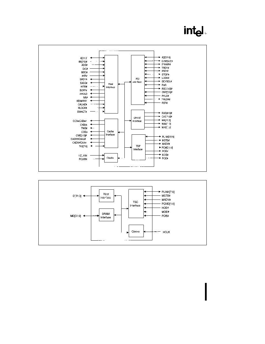
82437FX TSC Simplified Block Diagram
290518 ≠ 2
82438FX TDP Simplified Block Diagram
2

82430FX PCIset DATASHEET 82437FX SYSTEM
CONTROLLER (TSC) AND 82438FX DATA PATH UNIT (TDP)
CONTENTS
PAGE
1 0 ARCHITECTURE OVERVIEW OF TSC TDP
5
2 0 SIGNAL DESCRIPTION
6
2 1 TSC Signals
7
2 1 1 HOST INTERFACE (TSC)
7
2 1 2 DRAM INTERFACE (TSC)
8
2 1 3 SECONDARY CACHE INTERFACE (TSC)
9
2 1 4 PCI INTERFACE (TSC)
10
2 1 5 TDP INTERFACE (TSC)
11
2 1 6 CLOCKS (TSC)
11
2 2 TDP Signals
12
2 2 1 DATA INTERFACE SIGNALS (TDP)
12
2 2 2 TSC INTERFACE SIGNALS (TDP)
12
2 2 3 CLOCK SIGNAL (TDP)
12
2 3 Signal State During Reset
13
3 0 REGISTER DESCRIPTION
14
3 1 Control Registers
14
3 1 1 CONFADD
CONFIGURATION ADDRESS REGISTER
15
3 1 2 CONFDATA
CONFIGURATION DATA REGISTER
15
3 2 PCI Configuration Registers
16
3 2 1 VID
VENDOR IDENTIFICATION REGISTER
18
3 2 2 DID
DEVICE IDENTIFICATION REGISTER
18
3 2 3 PCICMD
PCI COMMAND REGISTER
18
3 2 4 PCISTS
PCI STATUS REGISTER
19
3 2 5 RID
REVISION IDENTIFICATION REGISTER
19
3 2 6 SUBC
SUB-CLASS CODE REGISTER
20
3 2 7 BCC
BASE CLASS CODE REGISTER
20
3 2 8 MLT
MASTER LATENCY TIMER REGISTER
20
3 2 9 BIST
BIST REGISTER
21
3 2 10 PCON
PCI CONTROL REGISTER
21
3 2 11 CC
CACHE CONTROL REGISTER
22
3 2 12 DRAMC
DRAM CONTROL REGISTER
23
3 2 13 DRAMT
DRAM TIMING REGISTER
24
3 2 14 PAM
PROGRAMMABLE ATTRIBUTE MAP REGISTERS (PAM 6 0 )
26
3 2 15 DRB
DRAM ROW BOUNDARY REGISTERS
29
3

CONTENTS
PAGE
3 2 16 DRT
DRAM ROW TYPE REGISTER
31
3 2 17 SMRAM
SYSTEM MANAGEMENT RAM CONTROL REGISTER
32
4 0 FUNCTIONAL DESCRIPTION
34
4 1 Host Interface
34
4 2 PCI Interface
34
4 3 Secondary Cache Interface
34
4 3 1 CLOCK LATENCIES
35
4 3 2 SNOOP CYCLES
35
4 3 3 CACHE ORGANIZATION
35
4 3 4 CLARIFICATION ON HOW TO FLUSH THE L2 CACHE
36
4 4 DRAM Interface
41
4 4 1 DRAM ORGANIZATION
41
4 4 2 MAIN MEMORY ADDRESS MAP
42
4 4 3 DRAM ADDRESS TRANSLATION
42
4 4 4 DRAM PAGE MODE
44
4 4 5 EDO MODE
45
4 4 6 DRAM PERFORMANCE
46
4 4 7 DRAM REFRESH
46
4 4 8 SYSTEM MANAGEMENT RAM
46
4 5 82438FX Data Path (TDP)
46
4 6 PCI Bus Arbitration
47
4 6 1 PRIORITY SCHEME AND BUS GRANT
47
4 6 2 CPU POLICIES
48
4 7 Clock Generation and Distribution
48
4 7 1 RESET SEQUENCING
48
5 0 PINOUT AND PACKAGE INFORMATION
49
5 1 82437FX Pinout
49
5 2 82438FX Pinout
53
5 3 82437FX Package Dimensions
55
5 4 82438FX Package Dimensions
57
6 0 82437FX TSC TESTABILITY
58
6 1 Test Mode Description
58
6 2 NAND Tree Mode
58
7 0 82438FX TDP TESTABILITY
64
7 1 Test Mode Description
64
7 2 NAND Tree Mode
64
4
82437FX TSC AND 82438FX TDP
1 0 ARCHITECTURE OVERVIEW OF
TSC TDP
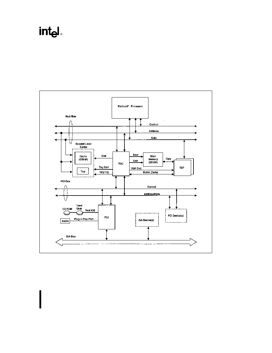
The 82430FX PCIset (Figure 1) consists of the
82437FX System Controller (TSC) two 82438FX
Data Path (TDP) units and the 82371FB PCI IDE
ISA Xcelerator (PIIX) The TSC and two TDPs form a
Host-to-PCI bridge The PIIX is a multi-function PCI
device providing a PCI-to-ISA bridge and a fast IDE
interface The PIIX also provides power manage-
ment and has a plug and play port
The two TDPs provide a 64-bit data path to the host
and to main memory and provide a 16-bit data path
(PLINK) between the TSC and TDP PLINK provides
the data path for CPU to PCI accesses and for PCI
to main memory accesses The TSC and TDP bus
interfaces are designed for 3V and 5V busses The
TSC TDP connect directly to the Pentium
proces-
sor 3V host bus The TSC TDP connect directly to
5V or 3V main memory DRAMs and the TSC con-
nects directly to the 5V PCI Bus
290518 ≠ 3
Figure 1 82430FX PCIset System
5