Other brands and names are the property of their respective owners
Information in this document is provided in connection with Intel products Intel assumes no liability whatsoever including infringement of any patent or
copyright for sale and use of Intel products except as provided in Intel's Terms and Conditions of Sale for such products Intel retains the right to make
changes to these specifications at any time without notice Microcomputer Products may have minor variations to this specification known as errata
November 1995
COPYRIGHT
INTEL CORPORATION 1996
Order Number 290219-006
82596DX AND 82596SX
HIGH-PERFORMANCE 32-BIT LOCAL
AREA NETWORK COPROCESSOR
Y
Performs Complete CSMA CD Medium
Access Control (MAC) Functions
Independently of CPU
IEEE 802 3 (EOC) Frame Delimiting
Y
Supports Industry Standard LANs
IEEE TYPE 10BASE-T (TPE)
IEEE TYPE 10BASE5 (Ethernet )
IEEE TYPE 10BASE2 (Cheapernet)
IEEE TYPE 1BASE5 (StarLAN)
and the Proposed Standard
TYPE 10BASE-F
Proprietary CSMA CD Networks Up
to 20 Mb s
Y
On-Chip Memory Management
Automatic Buffer Chaining
Buffer Reclamation after Receipt of
Bad Frames Optional Save Bad
Frames
32-Bit Segmented or Linear (Flat)
Memory Addressing Formats
Y
82586 Software Compatible
Y
Optimized CPU Interface
82596DX Bus Interface Optimized to
Intel's 32-Bit i386
TM
DX
82596SX Bus Interface Optimized to
Intel's 16-Bit i386
TM
SX
Supports Big Endian and Little
Endian Byte Ordering
Y
High-Performance 16- 32-Bit Bus
Master Interface
66-MB s Bus Bandwidth
33-MHz Clock Two Clocks Per
Transfer
Bus Throttle Timers
Transfers Data at 100% of Serial
Bandwidth
128-Byte Receive FIFO 64-Byte
Transmit FIFO
Y
Network Management and Diagnostics
Monitor Mode
32-Bit Statistical Counters
Y
Self-Test Diagnostics
Y
Configurable Initialization Root for Data
Structures
Y
High-Speed 5-V CHMOS
IV
Technology
Y
132-Pin Plastic Quad Flat Pack (PQFP)
and PGA Package
(See Packaging Specifications Order Number 240800-001
Package Type KU and A)
i386
TM
is a trademark of Intel Corporation
Ethernet is a registered trademark of Xerox Corporation
CHMOS is a patented process of Intel Corporation
290219 ≠ 1
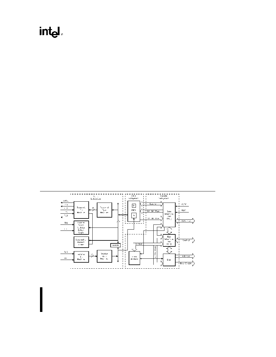
Figure 1 82596DX SX Block Diagram

82596DX SX
82596DX and 82596SX High-Performance
32-Bit Local Area Network Coprocessor
CONTENTS
PAGE
INTRODUCTION
3
PIN DESCRIPTIONS
10
82596 AND HOST CPU
INTERACTION
14
82596 BUS INTERFACE
14
82596 MEMORY ADDRESSING
14
82596 SYSTEM MEMORY
STRUCTURE
16
TRANSMIT AND RECEIVE MEMORY
STRUCTURES
17
TRANSMITTING FRAMES
20
RECEIVING FRAMES
21
82596 NETWORK MANAGEMENT AND
DIAGNOSTICS
21
NETWORK PLANNING AND
MAINTENANCE
23
STATION DIAGNOSTICS AND SELF-
TEST
24
82586 SOFTWARE COMPATIBILITY
24
INITIALIZING THE 82596
24
SYSTEM CONFIGURATION POINTER
(SCP)
24
Writing the Sysbus
25
INTERMEDIATE SYSTEM
CONFIGURATION POINTER
(ISCP)
26
INITIALIZATION PROCESS
26
CONTROLLING THE 82596DX SX
27
82596 CPU ACCESS INTERFACE
(PORT )
27
MEMORY ADDRESSING FORMATS
28
LITTLE ENDIAN AND BIG ENDIAN
BYTE ORDERING
28
COMMAND UNIT (CU)
29
RECEIVE UNIT (RU)
30
SYSTEM CONTROL BLOCK (SCB)
30
SCB OFFSET ADDRESSES
33
CONTENTS
PAGE
CBL Offset (Address)
33
RFA Offset (Address)
34
SCB STATISTICAL COUNTERS
34
Statistical Counter Operation
34
ACTION COMMANDS AND
OPERATING MODES
35
NOP
35
Individual Address Setup
36
Configure
37
Multicast-Setup
43
Transmit
44
Jamming Rules
46
TDR
47
Dump
49
Diagnose
52
RECEIVE FRAME DESCRIPTOR
52
Simplified Memory Structure
53
Flexible Memory Structure
54
Receive Buffer Descriptor (RBD)
55
PGA PACKAGE THERMAL
SPECIFICATION
60
ELECTRICAL AND TIMING
CHARACTERISTICS
60
Absolute Maximum Ratings
60
DC Characteristics
60
AC Characteristics
61
82596DX Input Output System
Timings
61
82596SX Input Output System
Timings
63
Transmit Receive Clock
Parameters
66
82596DX SX BUS OPERATION
68
System Interface A C Timing
Characteristics
69
Input Waveforms
70
Serial A C Timing Characteristics
72
OUTLINE DIAGRAMS
74
REVISION SUMMARY
77
2

82596DX SX
INTRODUCTION
The 82596DX SX is an intelligent high-performance
32-bit
Local
Area
Network
coprocessor
The
82596DX SX implements the CSMA CD access
method and can be configured to support all exist-
ing
IEEE
802 3
standards
TYPEs
10BASE-T
10BASE5 10BASE2 1BASE5 and 10BROAD36 It
can also be used to implement the proposed stan-
dard TYPE 10BASE-F The 82596DX SX performs
high-level commands command chaining and inter-
processor communications via shared memory thus
relieving the host CPU of many tasks associated
with network control All time-critical functions are
performed independently of the CPU this increases
network
performance
and
efficiency
The
82596DX SX bus interface is optimized for Intel's
i386
TM
DX and i386
TM
SX microprocessors
The 82596DX SX implements all IEEE 802 3 Medi-
um Access Control and channel interface functions
these include framing
preamble generation and
stripping source address generation destination ad-
dress checking short-frame detection and automat-
ic length-field handling Data rates up to 20 Mb s are
supported
The 82596DX SX provides a powerful host system
interface It manages memory structures automati-
cally with command chaining and bidirectional data
chaining An on-chip DMA controller manages four
channels this allows autonomous transfer of data
blocks (buffers and frames) and relieves the CPU of
byte transfer overhead Buffers containing errored or
collided frames can be automatically recovered with-
out CPU intervention The 82596DX SX provides an
upgrade path for existing 82586 software drivers by
providing an 82586-software-compatible mode that
supports the current 82586 memory structure The
82596DX SX also has a Flexible memory structure
and a Simplified memory structure The 82596DX
SX can address up to 4 gigabytes of memory The
82596DX SX supports Little Endian and Big Endian
byte ordering
The 82596DX SX bus interface is optimized to In-
tel's i386
TM
DX and i386 SX microprocessors pro-
viding a bus transfer rate of up to 66 MB s at
33 MHz The bus interface employs bus throttle tim-
ers to regulate 82596DX SX bus use Two large in-
dependent FIFOs
128 bytes for Receive and 64
bytes for Transmit
tolerate long bus latencies and
provide programmable thresholds that allow the
user to optimize bus overhead for any worst-case
bus latency
The 82596DX SX provides a wide range of diagnos-
tics and network management functions these in-
clude internal and external loopback exception con-
dition tallies channel activity indicators optional
capture of all frames regardless of destination ad-
dress (promiscuous mode) optional capture of er-
rored or collided frames and time domain reflectom-
etry for locating fault points on the network cable
The statistical counters in 32-bit segmented and lin-
ear modes are 32-bits each and include CRC errors
alignment errors overrun errors resource errors
short
frames
and
received
collisions
The
82596DX SX also features a monitor mode for net-
work analysis In this mode the 82596DX SX can
capture status bytes and update statistical coun-
ters of frames monitored on the link without trans-
ferring the contents of the frames to memory This
can be done concurrently while transmitting and re-
ceiving frames destined for that station
The 82596DX SX can be used in both baseband
and broadband networks It can be configured for
maximum network efficiency (minimum contention
overhead) with networks of any length Its highly
flexible CSMA CD unit supports address field
lengths of zero through six bytes for IEEE 802 3
Ethernet frame delimitation It also supports 16- or
32-bit cyclic redundancy checks The CRC can be
transferred directly to memory for receive opera-
tions or dynamically inserted for transmit operations
The CSMA CD unit can also be configured for full
duplex operation for high throughput in point-to-point
connections
The 82596 C-Step incorporates several new fea-
tures not found in previous steppings The following
is a summary of the 82596 C-step's new features
The 82596 C-step fixes Errata found in the A1
and B steppings
The 82596 C-step has improved AC timings over
both the A and B steppings
The 82596 C-step has a New Enhanced Big Endi-
an Mode where in Linear Addressing mode true
32-bit Big Endian functionality is achieved New
Enhanced Big Endian Mode is enabled by setting
bit 7 of the SYSBUS byte This mode is software
compatible with the big endian mode of the B-
step with one exception
no 32-bit addresses
need to be swapped by software in the C-step In
this new mode the 82596 C-step treats 32-bit ad-
dress pointers as true 32-bit entities and the SCB
absolute address and statistical counters are still
treated as two 16-bit big endian entities Not set-
ting this mode will configure the 82596 C-step to
be 100% compatible to the A1-step bit endian
mode
The 82596 C-step is hardware and software com-
patible to both the A1 and B steppings allowing
for easy ``drop-in'' to current designs Pinout and
control structures remain unchanged
The 82596DX SX is fabricated with Intel's reliable
5-V CHMOS IV (Process 648 8) technology It is
available in a 132-pin PQFP or PGA package
3


